
 Open Access Article
 This Open Access Article is licensed under a
 Creative Commons Attribution 3.0 Unported Licence
Novel 2D binning approach for advanced LIMS depth profiling analysis
Andreas
Riedo
 *a,
Valentine
Grimaudo
b,
Alena
Cedeño López
c,
Marek
Tulej
b,
Peter
Wurz
b and
Peter
Broekmann
c
*a,
Valentine
Grimaudo
b,
Alena
Cedeño López
c,
Marek
Tulej
b,
Peter
Wurz
b and
Peter
Broekmann
c
aSackler Laboratory for Astrophysics, Leiden Observatory, Leiden University, The Netherlands. E-mail: andreas.riedo@space.unibe.ch
bSpace Research and Planetary Sciences, Physics Institute, University of Bern, Switzerland
cInterfacial Electrochemistry Group, Department of Chemistry and Biochemistry, University of Bern, Switzerland
First published on 27th June 2019
Abstract
Spatially resolved chemical analysis of solids is of high interest and importance to various fields in industrial and academic research. In this contribution, we report on recent improvements in chemical depth profiling using Laser Ablation Ionization Mass Spectrometry (LIMS). More specifically, we compare two distinct depth profiling protocols, i.e., (i) the previously applied single crater analysis approach, and (ii) a novel multi-position binning mode for a layer-by-layer removal of sample material. Arrays of electrodeposited 50 μm-sized Sn/Ag solder bumps served as the test bed for method development. The presented studies show that the novel layer-by-layer approach outperforms the previously used single crater analysis protocol with regard to the analysis of non-uniformly distributed minor bulk species by increasing the lateral measurement spot statistics. Furthermore, with the application of single laser shots per surface position and subsequent translation to a new position, a signal enhancement of more than one decade is observed, which is especially important for monitoring low abundant elements in bulk material.
Introduction
In recent years, the application of measurement techniques that are coupled to a laser ablation source, e.g. Laser Ablation Inductively Coupled Plasma Mass Spectrometry (LA-ICP-MS), Laser Induced Breakdown Spectroscopy (LIBS) or Laser Ablation Ionisation Mass Spectrometry (LIMS), received increasing attention, particularly for the spatially resolved chemical analysis of industrially relevant materials, such as multi-layered devices from the microchip industry,1,2 photovoltaic cells3,4 or Li-ion batteries,5 to name just a few examples. LIMS also became an important technique supporting quality control and technological development. Besides the technical improvements of the instrumentation, which involve, amongst others, the detection sensitivity and the dynamic range of the analysers, also the commercialisation of new and less expensive femtosecond laser systems that, e.g., allow for a clean and controlled removal of the material significantly contributed to the popularity of this technique.6–10 The chemical analysis of solids by continuously applying a defined number of laser shots to a fixed surface position before changing to a proximal surface position (single crater analysis approach), e.g., ref. 11–13, and the layer-by-layer material removal strategy with single laser pulses per position and per layer14,15 are two commonly used measurement protocols that allow a 3D chemical reconstruction of the solid's composition. In the single crater analysis approach the pitch size between investigated surface positions is typically large enough to avoid any interference between adjacent laser ablation craters. Dedicated post-analysis approaches are often used to interpolate the recorded chemical information to provide the 3D fingerprint of the investigated analyte.5,14 To increase the lateral resolution, which is primarily limited by the diameter of the induced ablation crater, deconvolution models were developed for the analysis of measurement campaigns where laser ablation craters overlapped with each other.16In the past few years, substantial effort has been made in our laboratory to develop sophisticated measurement protocols for the LIMS technique17–20 dedicated to the chemical analysis of electrochemically fabricated samples, e.g. through-silicon-vias1 or lead-free solder bumps, which are relevant to the interconnect technology20 and typically have dimensions in the micrometre range. In this contribution, we discuss a new approach for the chemical depth profile analysis of Sn/Ag solder bumps (10 μm × Ø 50 μm) using LIMS, in which the so far applied 1D vertical analysis approach is extended to a 2D binning procedure where proximal surface locations are investigated by single laser shots and combined to a layer-by-layer single laser shot material removal strategy.
In comparison to the single crater depth profiling approach,11 spatially constrained inhomogeneities are averaged out due to the increased statistics, which provides an insight into the general trend of the element incorporation in the substrate material. Furthermore, the layer-by-layer approach allows recording measurements with a significant signal enhancement of more than one decade, mainly due to the increased material ablation if sampled over an extended area in comparison to the accumulation of mass spectra from a single surface position.
Experimental
Sample material and preparation
The specimens investigated in this contribution are Sn/Ag solder bumps (diameter: 50 μm, thickness: 10 μm) that were electrochemically deposited onto patterned Cu wafer coupons (imec, Leuven, Belgium). The wafer coupon comprises a 100 nm thick Cu seed layer, a 25 nm Ti buffer layer, and 100 nm Tix/SiO2 on a Si(100) substrate (see Fig. 1).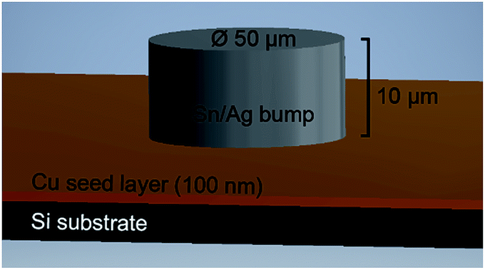 | ||
| Fig. 1 Schematics of the investigated Sn/Ag solder bumps. A layer of 10 μm Sn/Ag is electrochemically deposited on a Cu coupon. The Ti and Tix/SiO2 layers are not shown to simplify the image. | ||
A total open surface area of the wafer coupons of 0.02 cm2 (1′016 individual vias per 0.25 cm2) was exposed to the plating bath. A three-electrode setup was used for electrochemical deposition (ECD) consisting of the Cu wafer coupon as the working electrode, a Pt wire in a separate compartment as the counter electrode, and a double junction Ag/AgCl (3 M KCl) reference electrode (Metrohm Autolab B.V., The Netherlands). For plating experiments, the wafer coupons were fixed on a rotating disk electrode (RDE). All plating experiments were carried out under forced convective conditions at a given rotation speed of the RDE (800 rpm) and at a constant current density (−150 mA cm−2) supplied by a commercial potentiostat/galvanostat (Metrohm Autolab B.V., The Netherlands). Rotation of the working electrode was achieved with a rotator (Pine Research Instrumentation, USA).
LIMS instrument
The chemical depth profiling studies of the Sn/Ag solder bumps were carried out using a LIMS system discussed in detail in earlier publications.1,2,18,21,22 In the following, only a brief description about the measurement principle is given.The LIMS system comprises a miniature reflectron-type time-of-flight mass spectrometer and a femtosecond laser system21 that is coupled to a 3rd harmonic generator system (λ = 258 nm, 1 kHz repetition rate, pulse energies at the μJ level) to induce the ablation and ionisation process. The mass spectrometer is located within a vacuum chamber and a beam guiding system is used for laser beam delivery. The laser beam passes the entrance of the vacuum chamber and is focussed through the mass analyser towards the sample surface (laser ablation crater diameters of <10 μm) using a lens system that is installed on top of the instrument. After the ablation process the positively charged ions enter the ion optical system of the mass analyser, where they get accelerated, confined and focussed towards the field free drift path that separates ions according to their specific mass-to-charge ratio (time-of-flight (TOF) measurement principle).22 At the ion mirror, the ions are reflected backwards to the multi-channel plate detector system23 by passing the field free drift path again. The induced electric signals are recorded using a high-speed ADC system (up to 3.2 GS s−1, 12 bit vertical resolution). A quadratic equation mi(ti) = k0(ti − t0)2 is used for the conversion of the recorded TOF spectrum to the mass spectrum, where mi denotes an identified ion, ti its arrival time, and t0 and k0 the corresponding fit constants.22 The data analysis is realized using a software suite written in Matlab and developed within the last years in-house.24
Technical description of the measurement protocol
Chemical LIMS depth profiling studies have successfully been carried out on various materials, ranging from, e.g., geological samples containing putative fossils25 to materials of high interest to the semiconductor industry.1,18 Usually, these studies are performed by continuously firing a defined number of laser pulses at a given single surface location at a time before moving to a next surface location (named herein “single crater approach”). To further improve the LIMS chemical depth profiling, we went from the conventional measurement protocol to a layer-by-layer removal of sample material. For this purpose, an extended grid of locations for single laser shots, distributed over the surface area of interest, is applied to the specimen in a repetitive fashion. This grid of equidistant positions is provided by a Matlab-based software routine. The software first calculates a square-shaped grid of positions with a defined pitch distance. The definition of the pitch distance is crucial, as it determines the lateral overlap of adjacent craters at given instrument settings (e.g., lens system used for focussing, applied pulse energy). Grid positions that are not within the defined region of interest are subsequently rejected by the software. These input data are then loaded to the system control software that operates the laser system, the xy-translation stage for sample positioning, and the data acquisition system. Note that for each grid position only one single laser pulse is applied and one single TOF spectrum is recorded. As soon as all grid positions have been targeted by the laser (first layer completed), the control software automatically re-initiates the sampling of the same grid positions (start of the second layer, etc.). The user may define the number of sampling loops to be conducted. This number strongly depends on both sample specific characteristics (e.g., chemical nature and thickness of the sample) and laser specific parameters (e.g., applied laser pulse energy). The recorded data are finally loaded to an in-house written software package for detailed analysis.A main innovative feature of this new data processing software tool is the full freedom of data selection, which allows (i) for the re-construction of analogues to single crater depth profiles (single crater approach) on selected positions of the 2D grid, and (ii) for an averaging of the chemical composition within single layers of the targeted material (binning). The latter is enormously important, e.g. for interconnect features that were electrochemically processed through mask or Damascene plating approaches where global concentration gradients of trace and minor elements naturally appear along the surface normal. By this substantial improvement of measurement statistics, global trends in the concentration of minor and trace elements in the z-direction of the features can, for the first time, be discriminated from local variations of these elements within the xy-plane, in particular when comparing results of the single crater approach with those obtained for the layer-by-layer approach.
In Fig. 2, three different grid schemes with decreasing pitch distance are shown (selected area is 50 μm, fitted to the Sn/Ag solder bumps discussed earlier). By decreasing the pitch distance from 8 μm to 5 μm a significantly larger number of pixels is being gained (31 for 8 μm pitch in comparison to 80 for 5 μm pitch). In these schemes the grid position at the lower right corner is targeted first (red spot, bottom right panel in Fig. 2), and follows the red line on the left. After completion of all grid positions of the first layer the raster software initiates the second run for the second layer, which starts again on the first grid position indicated further down in red. The thickness of a layer is given by the ablation depth of the laser pulse at the selected intensity.
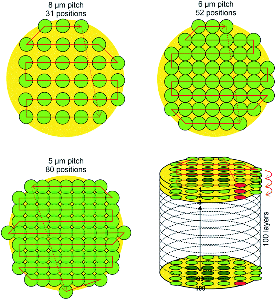 | ||
| Fig. 2 Schematics of three different grid layouts that are generated and placed over the target using the in-house written software suite. The decrease of the pitch size from 8 μm to 5 μm allows scanning the targeted area by 80 surface positions in comparison to 31 positions, respectively. At the bottom right, a schematic of the complete measurement protocol to measure multiple sample layers is illustrated, with the starting grid position highlighted in red. | ||
Measurements
Grid schemes with 8 μm, 6 μm and 5 μm pitch were selected for the testing of the newly developed software suite. The area of interest was constrained to 50 μm in diameter in accord with the grid schemes with 31, 52 and 80 surface positions. The applied pulse energies ranged from 0.27 μJ to 0.53 μJ. Stable pulse energies were reached by keeping the output power of the laser constant and using variable filter combinations. The applied number of investigated layers was between 30 and 100, depending on the experiments. Each fired laser pulse was further delayed by 100 ms, which allows for proper communication with the sample stage, the laser system, and the acquisition system including saving the data on the host computer. The single crater experiments were done at similar pulse energies and 1 kHz pulse repetition rate. The detailed experimental parameters are indicated in the corresponding figure captions. The signal gain of the new raster methodology was tested on a standard reference material (BCS-CRM No. 347, Bureau of Analysed Samples Ltd, Newham Hall, Newby, Middlesbrough, England, TS8 9EA) with similar bulk composition to the targeted Sn/Ag solder bumps.Results and discussion
Sample targeting
Recently, a high-resolution microscope camera system with imaging resolution of about 1 μm designed for ultra-high vacuum conditions was integrated in the current LIMS setup to allow accurate targeting of the desired positions on the sample.26 The microscope camera system is positioned next to the mass spectrometer, parallel to the ion optical axis of the mass spectrometer, which is about 70 mm away. A single laser ablation crater on the sample surface can be used for the calibration of the translation distance between the microscope and mass spectrometer (reproducibility of the position is 2.7 ± 1.2 μm). After calibration, the area of interest on the sample can be defined by first determining the coordinates of a solder bump centre.In Fig. 3, high-resolution scanning electron micrographs (SEM) of the three different grid schemes illustrated in Fig. 2 and applied to the Sn/Ag solder bumps are shown. In the top-down direction, the pitch distance decreases from 8 μm, to 6 μm and 5 μm, respectively. The red circles are given to guide the eyes and indicate the calculated grid positions and the actual laser spot size, which is currently below 10 μm in diameter. Each scanning loop was repeated 100 times, thus resulting in the complete removal of the sample material down to the Si wafer substrate (dark spots on the micrographs). In panel (a) the individual craters formed by the laser are clearly visible and well separated from each other. Using a pitch distance of 8 μm, an array of 31 individual craters was uniformly created on a circular area of 50 μm in diameter. A denser crater pattern is shown in panel (b) (52 positions per single ablation layer, 6 μm pitch), which represents an intermediate situation between well-separated and overlapping ablation craters. In this case, the pitch size was still slightly larger than the size of the laser ablation crater itself to avoid any overlap, but in comparison to panel (a) it is small enough to bring the craters in immediate proximity. The situation is different in panel (c) where a grid scheme was applied with slightly overlapping laser ablation craters. Note that an unintended offset in translation between the microscope and mass spectrometer resulted in the shift of the grid positions and the Sn/Ag solder bump. Nevertheless, in comparison to panels (a) and (b) the denser grid allows a more uniform removal of the target material. A small surface area covered by four grid positions can be observed in the panel indicating a leftover of the solder bump. This may be induced by irregularities within the material (e.g., harder localised grain).
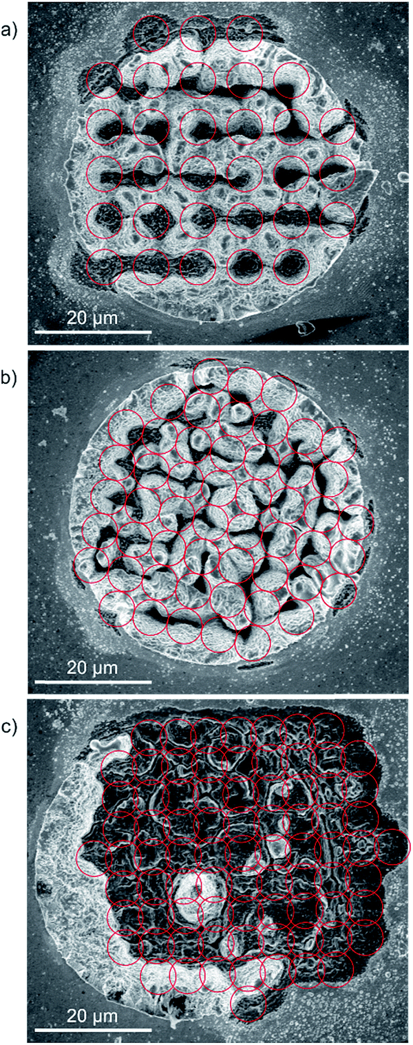 | ||
| Fig. 3 SEM images of Sn/Ag solder bumps after applying the three different grids illustrated in Fig. 2. From top to bottom the pitch size was decreased from 8 μm, to 6 μm, to 5 μm, respectively. The pulse energy was set in (a) to 0.46 μJ +/− 0.05 μJ, in (b) to 0.33 μJ +/− 0.03 μJ, and in (c) to 0.45 μJ +/− 0.04 μJ. Each grid cycle was repeated in all three cases 100 times. The denser the grid the more uniform is the overall removal of the material (compare panel (a) with no crater overlap and panel (c) with a slight overlap of grid positions). | ||
Improvement of bulk chemical depth profiling
Chemical depth profiling measurements on solder bumps considering only one sample location (analysis of one surface location along the z-axis, which is parallel to the surface normal) with a lateral resolution of better than 10 μm revealed an in-plane variation of the Ag content between individual single measurements. Material inhomogeneities at the micrometre scale that may be induced during the ECD clearly affect the chemical profile of such solder bumps and may lead to falsified interpretation of the deposition process. In panel (a) of Fig. 4 two chemical depth profiles of similar solder bumps measured at identical instrument settings are shown. The vertical lines indicate the interface layer between Sn/Ag and Cu, which is at a sample depth of 10 μm (see Fig. 1). The two depth profiles reveal a different distribution of the Ag content, which depends strongly on the location of the measurement. In the case of analysing a possible element abundance gradient of minor and trace elements along the z-axis, it is important to consider whether those species are homogeneously distributed within the sample or if they form aggregates in the bulk, e.g. accumulate at grain boundaries. Note that the smaller the analysis spot, the larger the impact of micrometre-large inhomogeneities. As an example, the individual chemical depth profiles in Fig. 4a would lead to a non-conclusive interpretation of the minor and trace elements (e.g. Ag) if only one single position would be considered. The combination of layer-by-layer analysis and the down-sampling of selected grid positions to 1D layer information allow us to significantly increase the statistics of the measurements and therefore the overall quality of the chemical depth profile; chemical depth profile outliers are simply averaged out. This measurement methodology can be compared to measurements conducted with Glow-Discharge Mass Spectrometry (GD-MS) where an area of mm2 size is investigated at once. In contrast, our LIMS instrument targets areas of μm2 size and additionally provides spatial composition information. The impact of this measurement procedure is visualized in Fig. 4, panel (b). Here, 31 positions were combined to one data point for one layer, and 100 layers were investigated in total. As a result, uniform increase of the abundance of minor bulk elements (e.g. Ag) towards the Cu seed at the bottom of the bump can be observed. The application of the layer-by-layer measurement protocol thereby allows improved understanding of the deposition process. The interpretation of the obtained data will be discussed in a follow-up contribution and is out of scope for this study.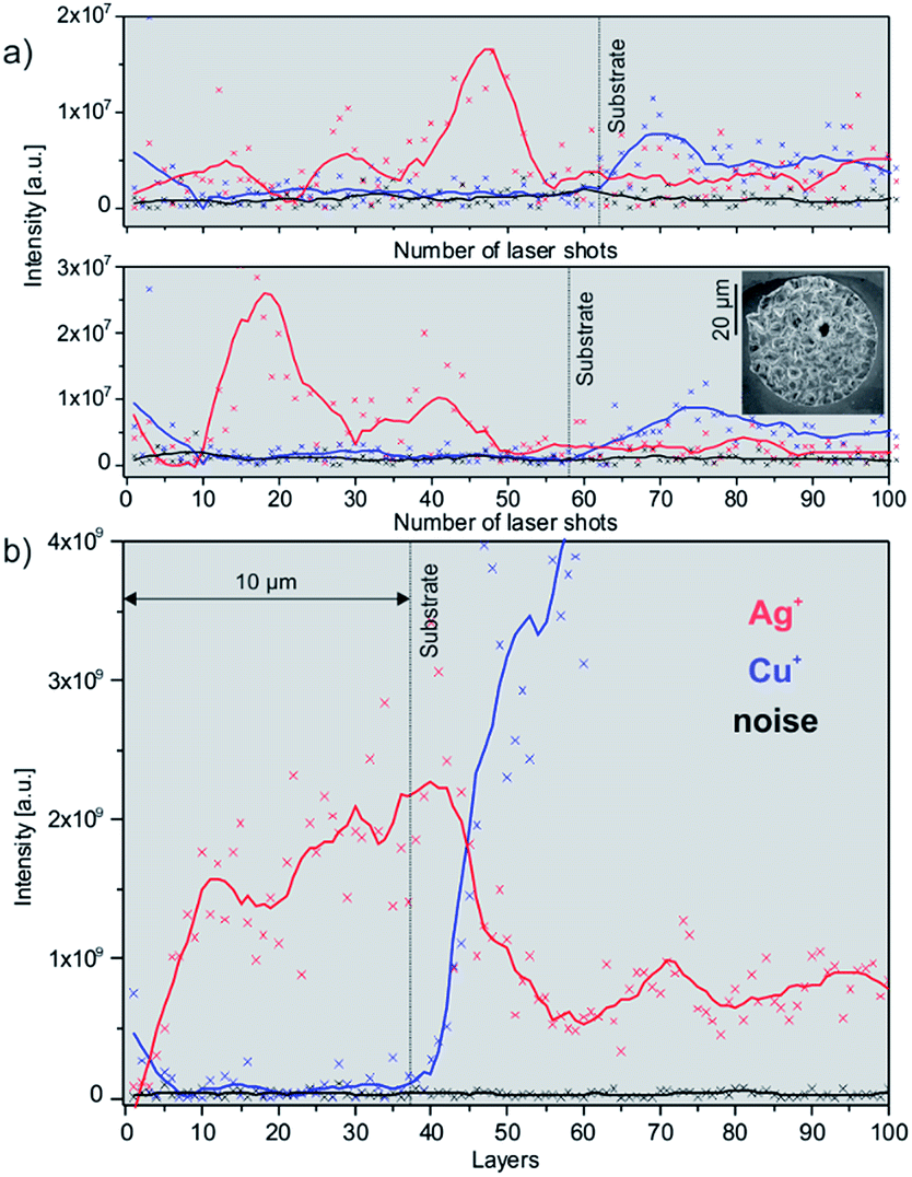 | ||
| Fig. 4 Chemical depth profile measurements of Sn/Ag solder bumps showing variations in the Ag+ and Cu+ contents. (a) Both panels show single position chemical depth profiles of two similar bumps; (b) layer-by-layer depth profiling approach. While in panel (a) two distinct Ag+ distributions along the sample depths are observed, a more uniform trend is visible in panel (b). The applied pulse energy in (a) was 0.54 μJ +/− 0.05 μJ, and in (b) was 0.46 μJ +/− 0.05 μJ. The grid scheme in (b) was 31 position/layer (see SEM in Fig. 3a). | ||
Improvement of measurement performance for bulk chemical analysis
The advantages and drawbacks of both measurement approaches for bulk chemical analysis were investigated conducting measurements on a certified standard reference material (BCS-CRM No. 347) with similar bulk composition to the analysed Sn/Ag bumps. In total 1′508 mass spectra were recorded for both protocols at similar measurement settings. In the case of single crater analysis mass spectra were recorded at 1 kHz pulse repetition rate whereas for the layer-by-layer approach mass spectra from 29 layers each consisting of 52 positions were acquired. In Fig. 5, the comparison between both measurement approaches is exemplified, showing a representative detail from the mass spectrum, the mass-to-charge range of Cu and Zn.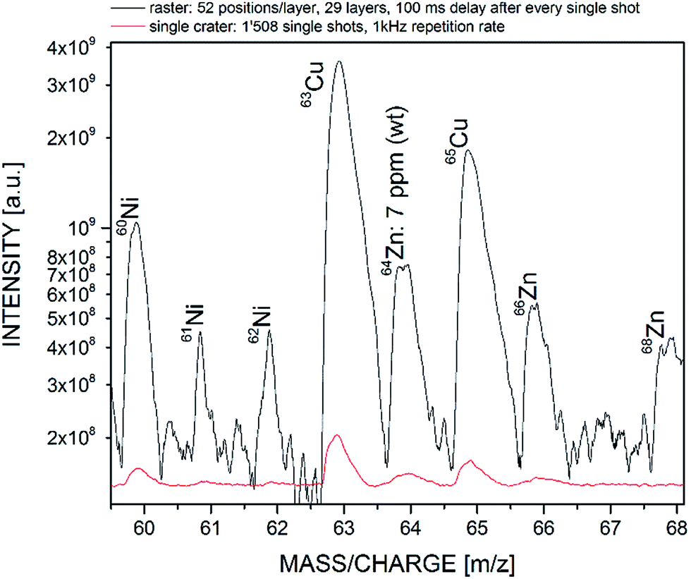 | ||
| Fig. 5 Comparison of measurement dynamics between single crater and layer-by-layer approach on a certified standard reference material (BCS-CRM No. 347) with similar bulk composition to the analysed Sn/Ag bumps. Averaging of the chemical information over an extended area allows us to record the measurement signal with an intensity increase of more than one order of magnitude, making less abundant peaks more visible. | ||
Compared to the single crater analysis, the layer-by-layer approach allowed us to record the chemical information of the bulk material with a signal enhancement of more than one order of magnitude. The improved performance allowed us to monitor e.g.64Zn with a sample weight abundance of 7 ppm much clearer as in the single crater campaign (note as well the logarithmic scale), and less abundant peaks, e.g. mass 61 or 62, become more visible as well. The significant increase of recorded signal is mainly due to the result of more ablated material and, to a lesser extent, to the recovery time of the multichannel plate detector system23 used in this instrument setup. In the case of Gaussian-like pulse profiles, the ablation of sample material decreases with increasing crater depth (no sample readjustment). Recent studies have demonstrated an exponential decrease of the ablation rate for Si and Cu substrates using the same instrument setup.27 This results in decreased recorded signal intensity and therefore in a lower signal-to-noise-ratio of the detected mass peaks. The lateral averaging of the material, in comparison, keeps the ablation plane at constant depth and therefore also the amount of ablated material. Furthermore, the recovery time of the multichannel plate detector may reduce as well the recorded signal, which is sampled at 1 kHz. It is well-known that the recovery times of such systems are in the order of ms and various models were developed for a better understanding and characterisation of such systems.28–32 Therefore, the operation of the laser system at a pulse repetition rate of 1 kHz (corresponding to 1 ms delay between each laser shot) may lead to undesired signal loss. Note that the communication to the sub-units in the layer-by-layer approach leads to total delays of ∼600 ms between each fired laser shot, which is sufficiently long to avoid potential gain reduction of the multichannel plate detector.
The software we developed allows us to select the regions of surface positions to be considered for the chemical analysis of a specimen, e.g., only a 2 × 2 position matrix or 4 × 4 grid. Analysis of the measurement campaign displayed in Fig. 5 shows that the SNR correlates with SNR(N) = a + bN0.5, where N denotes the number of recorded TOF spectra and a, b fit parameters (a ∼ 1.69, b ∼ 0.28) for the harmonic and the random noise, respectively. Note that we used the mass peak 60Ni for this analysis. In the case of purely random noise, we would expect that the fit parameter a would be 0, which would mean that the SNR increases with the square root of the number of recorded spectra. Non-random noise limits the increase of the SNR. At a certain point a significantly increased number of spectra would be required to improve the SNR only slightly, and may be even not feasible due to limited available surface area that can be sampled. However, the correlation provides a good estimate how much the SNR of a specific mass peak can be improved by increasing the number of recorded TOF spectra or how many spectra are required to record a certain peak at trace level abundance using this instrument setup.
The increased performance in the layer-by-layer approach, however, is at the expense of the required measurement time. While the single crater analysis measurement shown in Fig. 5 is accomplished only within few seconds (1′508 laser shots at 1 kHz pulse repetition rate last 1.5 s) the raster mode requires about 17 minutes. Nevertheless, e.g., for the composition analysis of layers containing trace elements with differential depth distribution this measurement strategy provides significant improvements.
Conclusions
Accurate chemical depth profiling analysis of complex materials is of high importance in numerous fields of academic and industrial research. Recent studies showed that our LIMS instrument has the capability to significantly contribute to the determination of the spatial chemical composition of solids relevant to the interconnect technology.In this contribution, we extended the standard 1D chemical depth profiling approach to a 2D binning procedure thus resulting in a layer-by-layer removal of target material with single laser shots per binned position. This novel approach shows in particular the capability to increase the measured signal intensity by more than one order of magnitude by simply averaging the chemical information in the lateral direction causing a significant improvement of the detection sensitivity for trace elements due to the increased signal-to-noise-ratios. The measurement protocol may also be used to minimise side-wall contributions in the case of overlapping laser ablation craters, which shall be addressed in future studies.
Earlier measurements showed that localised clustering of minor elements within the bulk of a solid material (e.g. by phase segregation) can substantially influence the compositional analysis of such highly heterogeneous target samples. The determination of the bulk composition can significantly be hampered or even be falsified when the elemental analysis is based on a single crater depth profiling approach only. This becomes particularly important when the dimension of the laser spot on the sample surface is in the lower micrometre range. By using the novel 2D binning approach the measurement statistics is substantially improved and the problems of the single crater approach are circumvented. This LIMS measurement methodology is a significant improvement, in particular for the future compositional analysis of interconnect features (Damascene, TSVs, solder bumps) where gradients of trace elements often appear along their main axes as a result of the additive-assisted electrodeposition process. The novel 2D binning approach of the LIMS depth profiling analysis will enable us to probe and quantify these concentration gradients with high accuracy, which is vital for any further improvement of these industrially relevant electroplating processes.
Conflicts of interest
There are no conflicts to declare.Acknowledgements
AR acknowledges the support from the European Union's Horizon 2020 research and innovation programme under the Marie Skłodowska-Curie grant agreement No. 750353. PW and PB acknowledge the support by the Swiss National Science foundation (SNSF).Notes and references
- V. Grimaudo, P. Moreno-García, A. Cedeño López, A. Riedo, R. Wiesendanger, M. Tulej, C. Gruber, E. Lörtscher, P. Wurz and P. Broekmann, Anal. Chem., 2018, 90, 5179–5186 CrossRef CAS PubMed.
- A. Riedo, V. Grimaudo, P. Moreno-Garcia, M. B. Neuland, M. Tulej, P. Wurz and P. Broekmann, J. Anal. At. Spectrom., 2015, 30, 2371–2374 RSC.
- A. Gutierrez-Gonzalez, C. Gonzalez-Gago, J. Pisonero, N. Tibbetts, A. Menendez, M. Velez and N. Bordel, J. Anal. At. Spectrom., 2015, 30, 191–197 RSC.
- S. Lee, J. J. Gonzalez, J. H. Yoo, J. R. Chirinos, R. E. Russo and S. Jeong, Thin Solid Films, 2015, 577, 82–87 CrossRef CAS.
- H. Hou, L. Cheng, T. Richardson, G. Chen, M. Doeff, R. Zheng, R. Russo and V. Zorba, J. Anal. At. Spectrom., 2015, 30, 2295–2302 RSC.
- V. Zorba, X. Mao and R. E. Russo, Spectrochim. Acta, Part B, 2015, 113, 37–42 CrossRef CAS.
- R. E. Russo, X. Mao, J. J. Gonzalez and S. S. Mao, J. Anal. At. Spectrom., 2002, 17, 1072–1075 RSC.
- R. Hergenröder, O. Samek and V. Hommes, Mass Spectrom. Rev., 2006, 25, 551–572 CrossRef PubMed.
- J. Pisonero and D. Günther, Mass Spectrom. Rev., 2008, 27, 609–623 CrossRef CAS PubMed.
- D. Käser, L. Hendriks, J. Koch and D. Günther, Spectrochim. Acta, Part B, 2018, 149, 176–183 CrossRef.
- V. Grimaudo, P. Moreno-García, A. Riedo, S. Meyer, M. Tulej, M. B. Neuland, M. Mohos, C. Gütz, S. R. Waldvogel, P. Wurz and P. Broekmann, Anal. Chem., 2017, 89, 1632–1641 CrossRef CAS PubMed.
- M. He, Y. Meng, S. Yan, W. Hang, W. Zhou and B. Huang, Anal. Chem., 2017, 89, 565–570 CrossRef CAS PubMed.
- J. T. van Elteren, A. Izmer, M. Šala, E. F. Orsega, V. S. Šelih, S. Panighello and F. Vanhaecke, J. Anal. At. Spectrom., 2013, 28, 994–1004 RSC.
- J. R. Chirinos, D. D. Oropeza, J. J. Gonzalez, H. Hou, M. Morey, V. Zorba and R. E. Russo, J. Anal. At. Spectrom., 2014, 29, 1292–1298 RSC.
- M. Burger, A. Gundlach-Graham, S. Allner, G. Schwarz, H. A. O. Wang, L. Gyr, S. Burgener, B. Hattendorf, D. Grolimund and D. Günther, Anal. Chem., 2015, 87, 8259–8267 CrossRef CAS PubMed.
- S. J. M. Van Malderen, J. T. van Elteren and F. Vanhaecke, Anal. Chem., 2015, 87, 6125–6132 CrossRef CAS PubMed.
- V. Grimaudo, P. Moreno-García, A. Riedo, A. C. López, M. Tulej, R. Wiesendanger, P. Wurz and P. Broekmann, J. Electrochem. Soc., 2019, 166, D3190–D3199 CrossRef CAS.
- V. Grimaudo, P. Moreno-García, A. Riedo, M. B. Neuland, M. Tulej, P. Broekmann and P. Wurz, Anal. Chem., 2015, 87, 2037–2041 CrossRef CAS PubMed.
- P. Moreno-García, V. Grimaudo, A. Riedo, M. Tulej, M. B. Neuland, P. Wurz and P. Broekmann, Electrochim. Acta, 2016, 199, 394–402 CrossRef.
- A. Cedeño López, V. Grimaudo, P. Moreno-García, A. Riedo, M. Tulej, R. Wiesendanger, P. Wurz and P. Broekmann, J. Anal. At. Spectrom., 2018, 33, 283–293 RSC.
- A. Riedo, M. Neuland, S. Meyer, M. Tulej and P. Wurz, J. Anal. At. Spectrom., 2013, 28, 1256–1269 RSC.
- A. Riedo, A. Bieler, M. Neuland, M. Tulej and P. Wurz, J. Mass Spectrom., 2013, 48, 1–15 CrossRef CAS PubMed.
- A. Riedo, M. Tulej, U. Rohner and P. Wurz, Rev. Sci. Instrum., 2017, 88, 045114 CrossRef PubMed.
- S. Meyer, A. Riedo, M. B. Neuland, M. Tulej and P. Wurz, J. Mass Spectrom., 2017, 52, 580–590 CrossRef CAS PubMed.
- M. Tulej, A. Neubeck, M. Ivarsson, A. Riedo, M. B. Neuland, S. Meyer and P. Wurz, Astrobiology, 2015, 15, 669–682 CrossRef CAS PubMed.
- R. Wiesendanger, D. Wacey, M. Tulej, A. Neubeck, M. Ivarsson, V. Grimaudo, P. Moreno, A. Cedeño López, A. Riedo and P. Wurz, Astrobiology, 2018, 18, 1071–1080 CrossRef CAS PubMed.
- V. Grimaudo, P. Moreno-García, A. C. López, A. Riedo, R. Wiesendanger, M. Tulej, C. Gruber, E. Lörtscher, P. Wurz and P. Broekmann, Anal. Chem., 2018, 90, 2692–2700 CrossRef CAS PubMed.
- J. Ladislas Wiza, Nucl. Instrum. Methods, 1979, 162, 587–601 CrossRef.
- G. W. Fraser, M. T. Pain, J. E. Lees and J. F. Pearson, Nucl. Instrum. Methods Phys. Res., Sect. A, 1991, 306, 247–260 CrossRef.
- A. Seko and H. Kobayashi, Rev. Sci. Instrum., 1973, 44, 400–405 CrossRef.
- A. S. Tremsin, J. F. Pearson, G. W. Fraser, W. B. Feller and P. White, Nucl. Instrum. Methods Phys. Res., Sect. A, 1996, 379, 139–151 CrossRef CAS.
- L. Giudicotti, M. Bassan, R. Pasqualotto and A. Sardella, Rev. Sci. Instrum., 1994, 65, 247–258 CrossRef.
| This journal is © The Royal Society of Chemistry 2019 |