
 Open Access Article
 This Open Access Article is licensed under a Creative Commons Attribution-Non Commercial 3.0 Unported Licence
Secondary ion mass spectrometry investigation of carbon grain formation in boron nitride epitaxial layers with atomic depth resolution†
Paweł Piotr
Michałowski
 *,
Piotr
Caban
and
Jacek
Baranowski
*,
Piotr
Caban
and
Jacek
Baranowski
Institute of Electronic Materials Technology, Wólczyńska 133, 01-919 Warsaw, Poland. E-mail: pawel.michalowski@itme.edu.pl
First published on 25th February 2019
Abstract
Secondary ion mass spectrometry (SIMS) measurements show that boron nitride (BN) films grown under an argon flow are contaminated with carbon in the form of clusters. SIMS imagining of carbon clusters with atomic depth resolution allows us to show that there are two different growth modes for BN films: 3D growth and self-terminated growth. The choice of the growth mode predominantly depends on reactor pressure. In the 3D growth mode (low pressure) carbon clusters appear in an organized way: the cluster in one BN layer nucleates the one in the successive layer. Eventually, they create three-dimensional carbon grains. In the self-terminated growth mode (high pressure) the distribution of carbon within the volume of the film is chaotic. The differences observed between the growth modes seem to depend on the diffusion length of the carbon and boron species.
1 Introduction
Two-dimensional (2D) materials and their heterostructures have attracted worldwide attention due to their remarkable optical, mechanical and electronic transport properties.1 Growth of 2D materials on insulating substrates is essential for the production of 2D devices on a commercial scale. Boron nitride (BN) with sp2-hybridized atomic sheets of boron and nitrogen is a particularly promising 2D material. It has a structure similar to that of graphene (1.7% lattice mismatch) but a wide band gap. Not only does BN have high thermal conductivity and high resistivity, but it has possibilities for integration with other 2D materials. Due to its sp2-hybridized bonding and weak van der Waals bonds, BN is an excellent candidate for use as a substrate and dielectric for graphene-based electronics.2 A great deal of effort has therefore been devoted to synthesizing BN films.The Metalorganic Chemical Vapour Deposition (MOCVD) method, well recognized for the epitaxial growth of III–V nitrides, is commonly used for the growth of BN epitaxial films.3 The most common substrate is sapphire – Al2O3 and precursors are triethylborane (TEB) for boron and ammonia (NH3) for nitrogen. There are several publications describing MOCVD growth on sapphire and other substrates.4–9 These earlier studies show a lack of surface uniformity of the BN films grown. A pulsed growth technique was also introduced for the deposition of BN, where the B metalorganics and ammonia are supplied to the reactor alternately. This reduces parasitic gas phase reactions.10–12 Important progress in the MOCVD growth of uniform BN films was achieved when it was demonstrated that the growth mode could be changed from 3D nucleation to 2D self-terminated nucleation by an increase in the V/III ratio and the use of high reactor pressure.13–16 The self-terminated growth mode with high reactor pressure resulted in atomically smooth 5–6 monolayer thick BN films. It was also found that substrate nitridation promotes self-terminating growth leading to atomically smooth films.16 Recently, it was reported that self-terminated behaviour is attributed to the fact that a sufficiently high NH3 partial pressure saturates the BN surface and prevents further absorption of boron precursors.17 However, this proposition does not explain why the growth stops after 5–6 layers. The detailed mechanism of BN growth and its change from 3D mode to self-terminated mode is still not understood.
In our previous work18 we showed that 3D growth and self-terminated growth under Ar flow lead to very high contamination by unreacted carbon. Secondary ion mass spectrometry (SIMS) measurements supported by several experimental techniques such as Scanning Electron Microscopy, X-Ray Reflectivity, Attenuated Total Reflectivity, Raman spectroscopy and Atomic Force Microscopy (AFM) have shown that the carbon appears predominantly in the form of clusters. Motivation behind the present work is to find how formation of carbon clusters takes place in the two growth modes of boron nitride. Distribution of these carbon clusters within the BN layers may be different under two growth modes. Such distribution was not measured up to now and due to significant improvement of our SIMS method it is now possible to get atomic resolution and thus obtain very precise information about carbon grain formation within BN layers.
2 Experimental
2.1 Sample preparation
Boron nitride films were grown on 2-inch double-sided polished (0001)-oriented Al2O3 with a maximum off-cut of 0.2° substrates using the MOCVD Aixtron Epigress VP508 system (horizontal, hot wall). A pulsed source injection mode with triethylborane (TEB) and ammonia (NH3) precursors was applied for suppressing gas phase prereactions. A single pulse consisted of the following steps: (1) TEB injection, (2) interruption, (3) NH3 injection, and (4) interruption.A high V/III ratio during the deposition at a temperature of 1050 °C was used for all the samples investigated. The BN layers were grown using argon as the carrier gas. The number of cycles was 800 for the three-dimensional growth mode (deposition at low pressure – 100 mbar and argon ambient) and 200 for the self-terminated growth mode (high pressure – 400 mbar and either argon or hydrogen ambient). Before the growth a thin, amorphous buffer layer was formed on the Al2O3 by a low temperature nitridation step. All growth parameters were kept the same in order to compare the carrier gas influence on the properties of the BN layers grown. Epilayers were cooled by NH3 and carrier gas flow.
2.2 Atomic force microscopy
AFM measurements were performed using a Bruker Dimension FastScan with ScanAsyst™, using silicon probes (Bruker OTESPA-R3 model) with a nominal force constant of 26 N m−1, and a typical nominal tip radius of 7 nm. The root mean square (RMS) roughness of the samples was measured over a scan area of 30 × 30 μm.2.3 Secondary ion mass spectrometry
In this work, all SIMS measurements were performed employing the CAMECA SC Ultra instrument under ultra-high vacuum (UHV), usually of 4 × 10⁻¹⁰ mbar. Sufficient depth resolution was obtained for the negative ion detection mode by using a low impact energy of 100 eV for a Cs+ primary beam rastered over 80 × 80 μm2. The analysis area was limited to 40 × 40 μm2. The SC Ultra tool is able to achieve such low impact energies due to the EXLIE (EXtra Low Impact Energy) technology, in the case of which a primary floating column concept is used.19 In this notion, contrary to standard SIMS tools, the primary column has the “floating voltage” instead of the grounded voltage level between the space at any two lenses inside the column and thus primary ions are slowed down at the end of the column maintaining favourable conditions for ion acceleration and beam stability. The ion beam on the sample in the SC Ultra tool has a square shape and due to the “variable rectangular shape concept” forms a homogeneous spot. The primary beam at a working point in the SC Ultra is formed by two stencils – well-shaped apertures. While the first one is used to choose the most intense and homogeneous part of the ion beam, the second one changes the size of the spot. These innovations allow one to use the low impact energy of primary ions with high sensitivity for all elements measured, high depth resolution (below 1 nm), and a high dynamic range with a low sputter rate.20,21 The electron gun was used to prevent charge build-up.To analyse each layer individually and reach atomic resolution, measurements were performed in two modes:
Even though the tool did not allow direct control over the incident angle, the desired value had been reached by changing the voltages applied to the accelerator, sample holder and primary column (floating voltage). Even though for the high incident angle the quality of the primary and secondary beam was not optimal, this mode was used to remove subsequent layers only so it was not an issue.
3 Results & discussion
SIMS is a very precise analytical technique for determining the elemental composition of a sample22–27 and it is especially well known for its excellent detection limits of trace elements.28–33 In our previous studies we have already presented the possibility of reaching nanometer and subnanometer depth resolution for the characterization of graphene34–38 as well as BN thin films.18 Therefore SIMS is a very good candidate for expanding this research and gaining some information about formation of carbon grains in boron nitride thin films.It has been noted experimentally that for a specific type of material – layered structures where the monolayers are held together by van der Waals (vdW) forces – secondary ion mass spectrometry measurements can reach atomic depth resolution as presented schematically in Fig. 1. The first layer is analysed in the static SIMS regime (the density of the beam is sufficiently low that less than 1% of the surface is damaged during the analysis). Then a short, dense pulse of primary ions with an extremely low impact energy (100 eV) and high incident angle removes the first layer completely without causing any significant damage to the second layer. Subsequent layers are similarly analysed in the static SIMS regime and then removed by a dense ion pulse. Such an extreme depth resolution can be reached only for two-dimensional van der Waals materials because the energy of the incoming ions will go to break up some covalent bonds in the first layer along with vdW bonds between the first and the second layer, as they are much weaker than covalent bonds (even up to three orders of magnitude) and are thus preferentially broken up. If the density and duration of the pulse are finely optimized the energy that is transferred to the sample is sufficient to sputter the first layer only. If a material consists of only covalent bonds then no bond will be preferentially broken up. A standard collision cascade will thus be generated and atoms from several monolayers will be sputtered, so the depth resolution will be lower.
 | ||
| Fig. 1 Secondary ion mass spectrometry with atomic resolution for two-dimensional van der Waals materials. The top layer is analysed in the static SIMS regime (less than 1% of the surface is bombarded) where a short pulse of primary ions with an extremely low impact energy and high incident angle removes the first layer completely without causing any significant damage to the second layer. With this approach each layer can be individually characterized and then removed. | ||
The possibility of reaching atomic depth resolution for SIMS measurements has been confirmed for multi-layer graphene and boron nitride thin films. This has been validated by AFM roughness measurements: for multi-layer graphene and boron nitride grown in self-terminated mode, RMS before and after SIMS experiments is the same, namely 0.15 ± 0.03 nm and 0.50 ± 0.05 nm, respectively. In the case of boron nitride grown in 3D mode, it has been observed that RMS slightly increases from 1.11 ± 0.07 nm to 1.20 ± 0.07 nm but the difference remains within standard deviation. It can be therefore concluded that this kind of SIMS measurement does not introduce any additional roughness and thus atomic depth resolution is indeed possible.
Out of these two materials the case of boron nitride is particularly interesting. Recent SIMS measurements have shown that the BN film grown under argon flow contains a high concentration of carbon, predominantly in the form of carbon clusters.18 It was proposed that the result of the reaction of two TEB molecules with ammonia molecules leads to BN and unreacted carbon. At that time, however, our SIMS procedure was not fully optimized and lateral imaging was not limited to a single layer of BN film. Reaching atomic resolution has allowed us to study carbon precipitates in detail. Fig. 2 presents a lateral distribution of carbon, boron and nitrogen for the third BN layer (counting from the surface) for a spot which was particularly contaminated. It can immediately be noted that the distributions of boron and nitrogen match very well. Analysing the distribution of nitrogen only may lead to the impression that the film is torn in some places. However, the nitrogen detection limit is very poor in this kind of measurement and the average intensity is only about 5 counts, and thus in some places no nitrogen signal has been detected even though boron has successfully been measured. This is just a measurement artifact and the distribution of boron should be treated as the most trustworthy signal to assess the quality of the BN film.
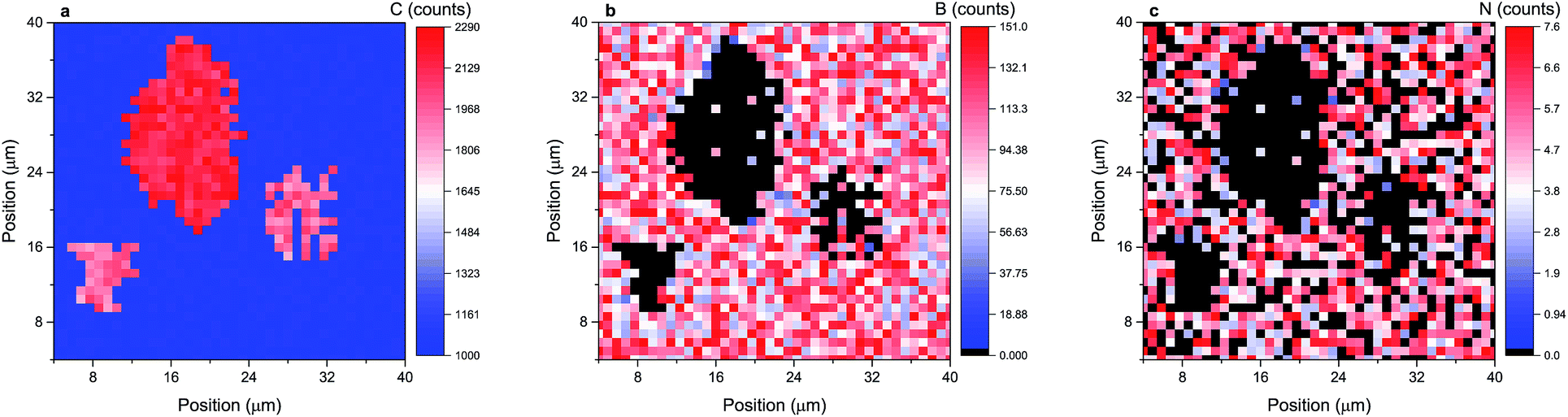 | ||
| Fig. 2 A lateral distribution of carbon, boron and nitrogen (a, b and c, respectively) for the third BN layer (counting from the surface) for a sample grown under high reactor pressure under Ar flow. | ||
The most important conclusion is that at the places where a significant amount of carbon has been detected both signals (those coming from B and N) equal zero or are at least very small, which means that no or a negligible amount of boron and nitrogen is present in the carbon precipitates. Similar carbon inclusions have already been analysed by high-resolution transmission electron microscopy.39 It should be emphasized, however, that atomic depth resolution of SIMS measurements is achieved at the expense of lateral resolution, which is in the range of a few microns. This means that the size of the registered carbon precipitates is artificially stretched out and that there may exist much smaller carbon inclusions which we cannot detect. In fact, a high intensity of the carbon signal on the whole area under analysis confirms the presence of many small carbon precipitates. They are not big enough to be directly imaged so the signal coming from them is averaged. Nevertheless the ability to image each BN layer separately, even with poor lateral resolution, may provide a lot of important information about the material.
Carbon precipitates can also be presented in a 3D view. To obtain the best possible image clarity we have followed a simple rule: if at one spot the intensity of the carbon signal is at least 1.5 higher than the average and at the same time the intensity of the boron signal is at least 0.5 smaller than the average then a colour voxel is used to denote high carbon content (the higher the intensity the brighter the voxel). In other cases, the voxel is transparent. Fig. 3a and b present a 3D visualization of carbon clusters within BN layers, which correspond to growth under low and high reactor pressure respectively. Simple inspection of these pictures clearly shows that there are basic differences between them. It can therefore be concluded that formation of carbon grains is indeed different in 3D mode and self-terminated mode.
 | ||
| Fig. 3 3D visualization of carbon clusters within BN layers. (a) In the case of low reactor pressure, carbon clusters appear in an organized manner and thus a large three-dimensional carbon pillar-shaped grain is formed. (b) In the case of high reactor pressure, carbon clusters present in the different BN layers are uncorrelated and appear in a chaotic way – carbon clusters have been marked with different colours for each layer. | ||
In the case of 3D growth, carbon clusters appear in an organized manner. They continue through the whole van der Waals structure eventually forming three-dimensional pillar-shaped carbon grains – this means that the carbon clusters in one BN layer have to be effective nucleation sites for the next BN layer. They reproduce themselves in successive BN layers, which means that formation of the next carbon cluster above the one beneath it has to be energetically favourable. This mode is characterised by low reactor pressure and thus one may assume that the diffusion length of carbon, boron and nitrogen species is relatively long, larger than the separation between carbon clusters. Therefore, the most energetically favourable nucleation site can be always decorated with carbon and boron species. Apparently, an ordered system of carbon clusters within van der Waals layers has to have lower energy than a chaotic system. SIMS maps show that eventually a large three-dimensional carbon grain is formed, as shown in Fig. 3a.
The situation is significantly different for growth under high reactor pressure (Fig. 3b), which leads to self-terminated mode. Carbon clusters present in the different BN layers are uncorrelated and appear in a chaotic way, contrary to what is observed in the case of 3D growth mode. Under high reactor pressure, a sufficiently high concentration of NH3 species on the surface of the BN layer may limit the diffusion of carbon and boron species. This will lead to a limited region for effective nucleation sites, the carbon and boron species having to choose a nucleation site in the vicinity of the region where the reaction between TEB and NH3 takes place.
It should be emphasized that the number of layers detected in each sample corresponds very well to the thickness of the BN film, namely 68 layers: ∼22 nm and 6 layers: ∼1.8 nm for samples grown under low and high reactor pressure respectively. This confirms that the established SIMS measurement procedure does indeed reach atomic depth resolution.
4 Conclusions
One of the main results of this work is the demonstration of SIMS as a useful technique for the investigation of 2D van der Waals materials. SIMS with atomic depth resolution has allowed the analysis of the composition and contamination content layer by layer. The detection of carbon clusters within successive layers has allowed us to study carbon grain formation in both 3D mode and self-terminated mode. The differences observed between the growth modes seem to depend on the diffusion length of the carbon and boron species.For low reactor pressure the diffusion length of the carbon and boron species is sufficiently long to find the most energetically convenient nucleation sites. These sites are connected with carbon clusters being in the lower BN layer. Nucleation sites will be reproduced from one layer to the next leading to carbon inclusions in the form of 3D carbon grains as shown in Fig. 3a and schematically in Fig. 4a. For high reactor pressure, due to the limited diffusion length of the carbon and boron species, there is no correlation between carbon grains in consecutive layers as shown in Fig. 3b and schematically in Fig. 4b.
 | ||
| Fig. 4 Schematic illustration of the formation of carbon grains in BN films. (a) For low reactor pressure, the diffusion length is high and thus each species can migrate to a favourable location and replicate the layer beneath. (b) For high reactor pressure, the diffusion length is limited and each atom is incorporated into the film in the vicinity of the region where the reaction between TEB and NH3 takes place. The distribution of carbon clusters is chaotic and there is no correlation between subsequent layers. | ||
Conflicts of interest
There are no conflicts to declare.Acknowledgements
This work was supported by the European Union's Horizon 2020 research and innovation programme under grant agreement No 785219.References
- K. S. Novoselov, A. Mishchenko, A. Carvalho and A. H. Castro Neto, Science, 2016, 353, aac9439 CrossRef CAS PubMed.
- C. Dean, A. Young, I. Meric, L. Wang, S. Sorgenfrei, K. Watanabe, T. Taniguchi, P. Kim, K. Shepard and J. Hone, Nat. Nanotechnol., 2010, 5, 3209 CrossRef PubMed.
- K. K. Kim, A. Hsu, X. Jia, S. M. Kim, Y. Shi, M. Dresselhaus, T. Palacios and J. Kong, ACS Nano, 2012, 6, 8583–8590 CrossRef CAS PubMed.
- T. Taniguchi, T. Sato, W. Utsumi, T. Kikegawa and O. Shimomura, Diamond Relat. Mater., 1997, 6, 1806–1815 CrossRef CAS.
- W. Gannett, W. Regan, K. Watanabe, T. Taniguchi, M. F. Crommie and A. Zettl, Appl. Phys. Lett., 2011, 98, 242105 CrossRef.
- J. Li, R. Dahal, S. Majety, J. Lin and H. Jiang, Nucl. Instrum. Methods Phys. Res., Sect. A, 2011, 654, 417–420 CrossRef CAS.
- M. Chubarov, H. Pedersen, H. HÃűgberg, J. Jensen and A. Henry, Cryst. Growth Des., 2012, 12, 3215–3220 CrossRef CAS.
- T. Doan, S. Majety, S. Grenadier, J. Li, J. Lin and H. Jiang, Nucl. Instrum. Methods Phys. Res., Sect. A, 2015, 783, 121–127 CrossRef CAS.
- S. K. Jang, J. Yuon, Y. J. Song and S. Lee, Sci. Rep., 2016, 6, 30449 CrossRef CAS PubMed.
- H. J. Kim, S. Choi, D. Yoo, J.-H. Ryou, R. D. Dupuis, R. F. Dalmau, P. Lu and Z. Sitar, Appl. Phys. Lett., 2008, 93, 022103 CrossRef.
- S. Majety, J. Li, X. K. Cao, R. Dahal, B. N. Pantha, J. Y. Lin and H. X. Jiang, Appl. Phys. Lett., 2012, 100, 061121 CrossRef.
- X. Yang, S. Nitta, K. Nagamatsu, S.-Y. Bae, H.-J. Lee, Y. Liu, M. Pristovsek, Y. Honda and H. Amano, J. Cryst. Growth, 2018, 482, 1–8 CrossRef CAS.
- Q. S. Paduano, M. Snure, J. Bondy and T. W. Zens, Appl. Phys. Express, 2014, 7, 071004 CrossRef.
- M. Snure, Q. Paduano, M. Hamilton, J. Shoaf and J. M. Mann, Thin Solid Films, 2014, 571, 51–55 CrossRef CAS.
- M. Snure, Q. Paduano and A. Kiefer, J. Cryst. Growth, 2016, 436, 16–22 CrossRef CAS.
- Q. Paduano, M. Snure, D. Weyburne, A. Kiefer, G. Siegel and J. Hu, J. Cryst. Growth, 2016, 449, 148–155 CrossRef CAS.
- A. Rice, A. Allerman, M. Crawford, T. Beechem, T. Ohta, C. Spataru, J. Figiel and M. Smith, J. Cryst. Growth, 2018, 485, 90–95 CrossRef CAS.
- P. Caban, D. Teklińska, P. Michałowski, J. Gaca, M. Wójcik, J. Grzonka, P. Ciepielewski, M. Możdżonek and J. Baranowski, J. Cryst. Growth, 2018, 498, 71–76 CrossRef CAS.
- CAMECA, Genneviliers, CAMECA SC-Ultra, User's Guide, 2005.
- D. Kouzminov, A. Merkulov, E. Arevalo and H. J. Grossmann, Surf. Interface Anal., 2013, 45, 345–347 CrossRef CAS.
- A. Merkulov, Surf. Interface Anal., 2013, 45, 90–92 CrossRef CAS.
- C. A. Andersen and J. R. Hinthorne, Science, 1972, 175, 853–860 CrossRef CAS PubMed.
- A. Benninghoven, Surf. Sci., 1975, 53, 596–625 CrossRef CAS.
- A. Benninghoven, F. G. Rudenauer and H. W. Werner, Secondary ion mass spectrometry: basic concepts, instrumental aspects, applications and trends, John Wiley & Sons, New York, 1987 Search PubMed.
- H. W. Werner, Surf. Sci., 1975, 47, 301–323 CrossRef CAS.
- H. Liebl, J. Vac. Sci. Technol., A, 1975, 12, 385 CrossRef CAS.
- H. Liebl, J. Appl. Phys., 1967, 38, 5277–5283 CrossRef CAS.
- K. Wittmaack, Appl. Phys. Lett., 1976, 29, 552 CrossRef CAS.
- B. Y. Ber, Y. A. Kudriavtsev, A. V. Merkulov, S. V. Novikov, D. E. Lacklison, J. W. Orton, T. S. Cheng and C. T. Foxon, Semicond. Sci. Technol., 1998, 13, 71–74 CrossRef CAS.
- C. Y. Chiou, C. C. Wang, Y. C. Ling and C. I. Chiang, Appl. Surf. Sci., 2003, 203–204, 482–485 CrossRef CAS.
- M. Emziane, K. Durose, D. P. Halliday, A. Bosio and N. Romeo, J. Appl. Phys., 2006, 100, 013513 CrossRef.
- T. Matsunaga, S. Yoshikawa and K. Tsukamoto, Surf. Sci., 2002, 515, 390–402 CrossRef CAS.
- H. Gnaser, Surf. Interface Anal., 1997, 25, 737–740 CrossRef CAS.
- P. Michałowski, W. Kaszub, A. Merkulov and W. Strupiński, Appl. Phys. Lett., 2016, 109, 011904 CrossRef.
- P. P. Michałowski, W. Kaszub, I. Pasternak and W. Strupinski, Sci. Rep., 2017, 7, 7479 CrossRef PubMed.
- P. P. Michałowski, I. Pasternak and W. Strupinski, Nanotechnology, 2018, 29, 015702 CrossRef PubMed.
- I. Grzonka, J. Pasternak, P. P. Michałowski, V. Kolkovsky and W. Strupinski, Appl. Surf. Sci., 2018, 447, 582–586 CrossRef.
- P. P. Michałowski, I. Pasternak, P. Ciepielewski, F. Guinea and W. Strupinski, Nanotechnology, 2018, 29, 305302 CrossRef PubMed.
- L. Ci, L. Song, C. Jin, D. Jariwala, D. Wu, Y. Li, A. Srivastava, Z. Wang, K. Storr, L. Balicas, F. Liu and P. Ajayan, Nat. Mater., 2010, 9, 430–435 CrossRef CAS PubMed.
Footnote |
| † Electronic supplementary information (ESI) available. See DOI: 10.1039/c9ja00004f |
| This journal is © The Royal Society of Chemistry 2019 |