 Open Access Article
 This Open Access Article is licensed under a
 Creative Commons Attribution 3.0 Unported Licence
Spike sorting using non-volatile metal-oxide memristors†
Isha
Gupta
*,
Alexantrou
Serb
,
Ali
Khiat
,
Maria
Trapatseli
and
Themistoklis
Prodromakis
Electronic Materials and Devices Research Group, Zepler Institute for Photonics and Nanoelectronics, University of Southampton, SO17 1BJ, Southampton, UK. E-mail: I.Gupta@soton.ac.uk
First published on 23rd November 2018
Abstract
Electrophysiological techniques have improved substantially over the past years to the point that neuroprosthetics applications are becoming viable. This evolution has been fuelled by the advancement of implantable microelectrode technologies that have followed their own version of Moore’s scaling law. Similarly to electronics, however, excessive data-rates and strained power budgets require the development of more efficient computation paradigms for handling neural data in situ; in particular the computationally heavy task of events classification. Here, we demonstrate how the intrinsic analogue programmability of memristive devices can be exploited to perform spike-sorting on single devices. Leveraging the physical properties of nanoscale memristors allows us to demonstrate that these devices can capture enough information in neural signal for performing spike detection (shown previously) and spike sorting at no additional power cost.
A Introduction
Spike sorting is the procedure of identifying the activity of individual neurons from data collected through electrophysiological experiments.1–7,13–16 Typically, this involves processing raw neuronal data by first detecting the presence of action potential (spiking) activity, then extracting appropriately chosen features and finally, clustering the results;10,11 each cluster corresponding to an individual neuron.Memristive devices can inherently act as thresholded integrators.17 These metal-oxide-metal resistive switching devices exhibit non-volatile behaviour performing a dual function of computation and storage at the same site. When presented with an input voltage waveform the devices accumulate changes in resistive state linked to the instantaneous signal magnitude and polarity, so long as this exceeds the device threshold. We recently exploited this property for detecting neuronal spiking activity8 while filtering out background noise.
In this work, the capability of single memristive devices to act as spike-sorting elements was experimentally demonstrated using a commercially available memristor characterisation instrument. Publicly available simulated neural signals constructed based on electrophysiological recordings from the cortex and basal ganglia15 were used as the input data for the memristive spike sorter. The data essentially contained three distinct single-unit activity waveform prototypes overlaid on a noise background. The instrument applied suitable amplification and relayed these waveforms to stand-alone devices.
B Methods
Memristive devices and hardware instrumentation
For all experiments in this work, bilayer metal-oxide memristors were used with stack configuration Pt/AlOx/TiOx/Pt (10/4/40/10 nm) (see Fig. 1(a)). Patterning was carried out using conventional optical lithography and lift-off processes. The electrodes were deposited using e-beam evaporation while the oxides were fabricated using magnetron sputtering. Electrical characterisation was carried out using a memristor characterisation and testing platform featuring ArC instruments Ltd. Technology (https://www.arc-instruments.co.uk/, ESI Fig. 1†). The instrument can be used to characterise devices both in-package and directly on-wafer via probe card. For the demonstrated experiments, both packaged and on-wafer devices were used.18 Before use, all devices had to be electroformed; a one-time process that electrochemically activates the memristor.19 Our test devices typically electroform once at 8–12 V. Once electroformed, the devices show reliable, well-behaved switching in the [+1.2, +2.5] V and [−1.2, −2.5] V ranges. For this work, the devices were used in the 5–20 kΩ resistive state operating range. | ||
| Fig. 1 Memristive devices and neural signals. (a) Simplified schematic of experimental set-up. The top electrode of each test device was grounded whilst suitably amplified neural signal data samples were applied to the bottom electrode. Inset: atomic force microscopy image of memristive devices. (b, d and f) Neural signal data used as input to the memristive spike sorter. Each panel corresponds to neural spikes generated by different neurons and consequently featuring different signature waveforms. Thick traces: average spike waveform for each class (average of 10 instances). Thin traces: 10 different individual instances of spikes (c, e and g). Data includes amplification as shown in (a). Response of memristive devices to inputs from (b, d, and f) respectively. Memristor resistive state jumps are observed in tight correlation to input signal voltage peaks. Pink dots: measured resistive state values. Blue: spike type/class I. Red: type II. Green: type III. | ||
Neural data source
The neural data used for our experiments is publicly available from the University of Leicester, R. Q. Quiroga group (https://www2.le.ac.uk/centres/csn/software);15 dataset no. 2. It consists of a simulated neural recording synthesised using three distinct single-unit activity templates (extracted from measured data) overlaid on top of background noise. We refer to each unique combination of a standardised spike waveform plus noise as a ‘spike instance’.Memristive based spike-sorter
A simplified system schematic for the memristor based spike-sorter8 is presented in Fig. 2(a). The setup for acquiring/recording neural data (for instance a CMOS based front-end system) is external to the presented memristor-based spike-sorter. In this work, neural input data used for the experiments was stored on a PC. Data entering the memristor-based spike-sorter is first subjected to amplification and offset (i). The appropriate degree of amplification is determined following the thresholded integrator property of memristive devices: significant neural activity (spikes) must lie above the switching threshold of the device whilst noise should remain below it.8,9 In the second stage (ii), the conditioned waveforms are fed to the memristive devices using the characterisation instrument and the resistive state of the device is read periodically. The presence of supra-threshold spikes in the input is expected to cause significant changes in the resistive state of the device whilst the background noise will be inherently suppressed. Finally (iii), all captured resistive states are post-processed in order to estimate the number and identities of the spikes present.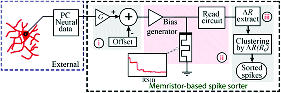 | ||
| Fig. 2 Memristive based spike-sorter. This figure has been duplicated from author’s previous work.8 | ||
Memristive based spike-sorter signal processing
Signal-processing strategy for a memristor-based spike sorter is discussed in detail in our previous work.8 To summarise, a figure is appended in ESI Fig. 2.† Briefly, the entire neural signal is passed through the devices in small snippets i.e. ‘batches’. These batches are further sub-divided into smaller ‘bins’. At the end of each bin, the resistive state of the device is read and recorded (at low read voltages of 0.2 V). The resistive state read before and after a bin facilitates the estimation of change of resistive state in each bin. For estimation of noise baseline, after every batch, the neural signal is paused and the state of the device is recorded.For spike sorting, the changes in resistive state registered in each bin are plotted as a function of the initial resistive state of each bin.
C Results
The capability of single memristive devices to act as spike-sorting elements was experimentally demonstrated using a commercially available memristor characterisation instrument. Publicly available simulated neural signals constructed based on electrophysiological recordings from the cortex and basal ganglia15 were used as the input data for the memristive spike sorter (Fig. 1b, d and f and ESI Fig. 3†). The data contained three distinct single-unit activity waveform prototypes overlaid on a noise background. For each prototype, ten random instances were chosen and the values were then averaged (indicated as thick lines in Fig. 1). The exact time instances of the randomly chosen spike waveforms are indicated in Tables 1 and 2. The tables also indicate maximum and minimum values of each averaged spike prototype. The instrument applied suitable amplification as explained in the methods section and relayed these waveforms to stand-alone memristive devices.| S. no. | Average spike prototypes | Max. (V) | Min. (V) |
|---|---|---|---|
| 1 | Spike prototype 1 | 1.04 | −0.33 |
| 2 | Spike prototype 2 | 0.97 | −0.52 |
| 3 | Spike prototype 3 | 0.85 | −0.30 |
| S. no. | Spike waveform 1 (spike timings) | Spike waveform 2 (spike timings) | Spike waveform 3 (spike timings) |
|---|---|---|---|
| 1 | 2785 | 20![[thin space (1/6-em)]](https://www.rsc.org/images/entities/char_2009.gif) 173 173 |
45450 |
| 2 | 54871 |
41370 |
465326 |
| 3 | 127642 |
107486 |
606816 |
| 4 | 207821 |
194634 |
854280 |
| 5 | 395160 |
300366 |
939685 |
| 6 | 708914 |
395161 |
1091743 |
| 7 | 903698 |
631599 |
1208267 |
| 8 | 1011435 |
886880 |
1314658 |
| 9 | 1273906 |
1082916 |
1436188 |
| 10 | 1420564 |
1330703 |
204139 |
Experiment I
For the first experiment, the averages of each of the three single-unit waveforms were obtained by pooling ten random instances from each class. These were then arranged in a spike triplet as shown in Fig. 3(a) and 4, at the end of which a reset pulse was appended. The justification for adding a reset pulse of the opposite polarity is to mitigate the effects of device resistive state saturation.9 An exemplary figure has been added in ESI Fig. 5.† Continuous operation of the memristive device in the non-volatile regime for input signals dominated by peaks of a single polarity results in saturation of the resistive state of the device. Furthermore, to test the repeatability, ten spike triplets were sequentially fed into the test memristor and its resistive state was regularly assessed 3 times during each triplet, producing results similar to Fig. 1(b–g) (amplification gain: −1.3 offset: −0.63 V). The devices were reset after each spike triplet and not after each spike waveform. The change in resistive state between every pair of consecutive measurements vs. the resistive state in the first measurement of the same pair results in Fig. 3(b and d). More clearly, the resistive state change measured between the beginning and the end of a spike waveform was plotted as a function of its initial resistive state. | ||
| Fig. 3 Spike sorting using memristive devices. (a and c) Input waveform for the repeatability experiment. The waveform contains 10 identical copies of a spike triplet. Each triplet contains a succession of three different spike waveforms and is terminated by a reset pulse (example highlighted in yellow). Averaged spike waveforms were used in this case (thick traces in Fig. 1(b, d and f)). Arrows and numbers indicate the timing and waveform class of each spike within a triplet. (b) Summary of results. Change in resistive state vs. starting resistive state for each pair of consecutive measurements taken whilst the input from (a and c) was applied to the memristive device (see Fig. 1(c, e and g) and main text for details). The emergence of three distinct clusters of data-points corresponding to the three input spike classes is observed. Colour code represents five different spike triplets. (d) Three different clusters with respect to spike type (I, II and III). Highlighted data-points (black outline): points gathered while applying the 8th triplet as input. | ||
 | ||
| Fig. 4 (a) Input signal used for Fig. 3. Ten copies of a spike triplet were concatenated and fed to the device-under-test. The triplet was composed of the three average spike prototypes arranged in increasing order of amplitude i.e. order 3, 2, 1. Reset pulses followed every spike triplet. This stimulus was chosen in order to experimentally demonstrate the response repeatability of the device-under-test. (b) Resistive state evolution of the device in response to the neural recording in (a). | ||
These results capture the impact of each spike’s strength on setting the memory state of the device with respect to its initial state, as exemplified by the spike triplets in Fig. 3(a) and their corresponding R(ΔR) points in Fig. 3(b) [initial resistance vs. fractional changes in resistive state]. For a raw data example, i.e. method of estimating the fractional change in the resistive state, see ESI Table 1.† The clear clustering of the data-points associated with the three distinct spike waveform prototypes as illustrated in Fig. 3(d) demonstrates that the memristive device is capable of intrinsically performing spike sorting consistently. As the waveform input to the device is identical for each triplet, any variation in R(ΔR) response arises mainly from device variability.
Experiment II
For the second experiment, the triplets were constructed from individual spike instances (not averaged prototypes) and their order was randomised as shown in Fig. 5(a and c) and 6. This setup accounts for background noise-induced spike shape variability.15 The results are shown in Fig. 5(b and d) and ESI Table 2,† where the intrinsic variability in device behaviour is compounded by the variability in the spike waveforms. Notably, despite the fact that clustering has smeared and is no longer as clear as in Fig. 3(b and d), it is still possible to linearly separate the majority of events. The misclassified spike that caused strong change in resistive state (enclosed in a box) was the result of the event instance containing two spikes in close succession (main spike plus a stray spike). | ||
| Fig. 5 (a and c) Input waveform consisting of ten triplets, each constituted by random spike instances appearing in randomised order. (b) Corresponding results. Change in resistive state vs. starting resistive state for each pair of consecutive measurements taken whilst the input from (b and d) was applied to the memristive device. The variability introduced by the input waveforms scatters the clusters, which, however, remain broadly linearly separable. Boxed data point: the spike instance waveform contained a double spike (spike triplet 6 – highlighted in (c) in grey). (d) Three different clusters with respect to spike type (I, II and III). | ||
 | ||
| Fig. 6 (a) Neural waveform used for Fig. 5. Randomly chosen spike waveform instances, one belonging to each prototype, were arranged in random order as shown in the figure in order to form a spike triplet. Reset pulses followed every spike triplet. Ten such randomly generated triplets were concatenated and fed to the device-under-test. (b) Resistive state evolution of the device in response to the neural recording in (a). | ||
The prototype devices used for experiments show intrinsic variability and a range of variation in threshold voltages, however, since we assess the fractional changes in the resistive change of the device, the variability factor is compensated to a certain extent. One possible solution in the future will be to use alternative or engineered materials as the devices active core, which could potentially allow innovations to achieve a smaller range of variations in threshold voltages. Equally important, the use of reset pulses is mandatory for non-volatile memristive devices for compensating the saturating behaviour of devices.9 Better solutions in this respect can be found by employing memristive devices operating in the volatile region.20 Exploiting this completely different behaviour of the devices might eliminate the need for reset pulses making the implementation of this technology much more power efficient. Moreover, we do note that signal artefacts related with the employed recording methodology will overall contribute to an increase in detecting false positive events. Our approach can be tailored via gain adjustment to be immune to power-line noise and EM interference, nonetheless, large-amplitude and/or stimulation artefacts would require additional pre-filtering that is commonly used in other spike-detection implementations.
Memristive devices are sensitive to the envelope of the spike waveform, where resistive state change of the device depends on spike amplitude, polarity, and width. The results presented in this manuscript is our initial work at ‘proof-of-concept’ level. Many significant questions, such as how will the devices be integrated at the system level or how devices will perform in cases where action potentials with different shapes but same amplitude exist, remain as the future work. To a certain extent, the nature of spike sorting also depends upon the number of questions, such as the application/disease under study, the nature of the recording, i.e. intracellular or extracellular, assessing if the recording contains multi-unit activity or single-unit activity, or the compound action potentials. Therefore, to assess the performance of devices in all such scenarios more closely, we aim to study this subject in-depth in the near future.
D Conclusions
In conclusion, we demonstrate that memristor-based spike sorting systems are promising candidates for future brain-machine interfaces. The spike sorting ability of the concept systems presented here is compounded by the positive downscaling prospects of memristive technologies, both in area12 and power.21 Our results prove that single nanometre scale devices can capture enough input signal information for encoding distinct spike classes at no extra power (∼100 nW)20 or area cost to what we have shown previously for spike detection.17,20 Our results bring new application prospects for memristive devices, diversifying from conventional digital memory applications towards enabling active neural interfacing technologies that are very much needed for realising the electroceuticals vision.22Author Contributions
I. G. and T. P. conceived the experiments. A. S. provided the hardware/instrumentation used for experiments. A. K. and M. T. fabricated and optimised the devices. I. G. carried out the experiments, performed the data analysis and wrote the manuscript.Conflicts of interest
The authors declare no competing financial interests.Acknowledgements
We acknowledge the financial support of FP7 RAMP and EPSRC EP/K017829/1 and EP/R024642/1. The datasets used for the experiments in the manuscript are publicly available from the R. Q. Quiroga group at the University of Leicester (dataset 2).References
- M. A. Lebedev and M. A. L. Nicolelis, Brain-Machine Interfaces: From Basic Science to Neuroprostheses and Neurorehabilitation, Physiol. Rev., 2017, 97, 767–837 CrossRef PubMed.
- A. K. Bansal, W. Truccolo, C. E. Vargas-Irwin and J. P. Donoghue, Decoding 3D reach and grasp from hybrid signals in motor and premotor cortices: spikes, multiunit activity, and local field potentials, J. Neurophysiol., 2012, 107, 1337–1355 CrossRef PubMed.
- F. Franke, et al., High-density microelectrode array recordings and real-time spike sorting for closed-loop experiments: an emerging technology to study neural plasticity, Front. Neural Circuits, 2012, 6, 1–7 Search PubMed.
- C. M. Lopez, et al., A 966-electrode neural probe with 384 configurable channels in 0.13 μm SOI CMOS, 2016 IEEE Int. Solid-State Circuits Conf., 2016, pp. 392–393, DOI:10.1109/ISSCC.2016.7418072.
- B. K. D. Wise, et al., Microelectrodes, Microelectronics, and Implantable Neural Microsystems, Proc. IEEE, 2008, 96, 1184–1202 Search PubMed.
- Ian H. Stevenson and K. P. Kording, How advances in neural recording affect data analysis, Nat. Neurosci., 2011, 14, 139–142 CrossRef CAS PubMed.
- A. Berényi, Z. Somogyvári, A. J. Nagy, L. Roux, J. D. Long, S. Fujisawa, E. Stark, A. Leonardo, T. D. Harris and G. Buzsáki, Large-scale, high-density (up to 512 channels) recording of local circuits in behaving animals, J. Neurophysiol., 2014, 111, 1132–1149 CrossRef PubMed.
- I. Gupta, et al., Real-time encoding and compression of neuronal spikes by metal-oxide memristors, Nat. Commun., 2016, 7, 1–16 Search PubMed.
- I. Gupta, A. Serb, A. Khiat and T. Prodromakis, Improving detection accuracy of memristor-based bio-signal sensing platform, IEEE Trans. Biomed. Circuits Syst., 2016, 1–9, DOI:10.1109/TBCAS.2016.2580499.
- I. Gupta, S. Alexantrou, A. Khiat and T. Prodromakis, Towards a memristor-based spike-sorting platform, IEEE Biomed. Circuits Syst., pp. 1–4, 2016 Search PubMed.
- M. S. Lewicki, A review of methods for spike sorting: the detection and classification of neural action potentials classification of neural action potentials, Netw. Comput. Neural Syst., 1998, 9(4), R53–R78 CrossRef CAS.
- A. Khiat, P. Ayliffe and T. Prodromakis, High Density Crossbar Arrays with Sub-15 nm Single Cells via Liftoff Process Only, Sci. Rep., 2016, 6, 32614 CrossRef CAS PubMed.
- H. G. Rey, C. Pedreira and R. Quian Quiroga, Past, present and future of spike sorting techniques, Brain Res. Bull., 2015, 119, 106–117 CrossRef PubMed.
- M. Mahmud and S. Vassanelli, Processing and analysis of multichannel extracellular neuronal signals: state-of-the-art and challenges, Front. Neurosci., 2016, 10, 1–12 Search PubMed.
- R. Q. Quiroga, Z. Nadasdy and Y. Ben-Shaul, Unsupervised spike detection and sorting with wavelets and superparamagnetic clustering, Neural Comput., 2004, 16, 1661–1687 CrossRef PubMed.
- R. Quian Quiroga, What is the real shape of extracellular spikes?, J. Neurosci. Methods, 2009, 177, 194–198 CrossRef CAS PubMed.
- I. Gupta, et al., Real-time coding and compression of neuronal spikes by metal-oxide memristors, Nat. Commun., 2016, 7, 12805 CrossRef CAS PubMed.
- A. Serb, R. Berdan, A. Khiat, C. Papavassiliou and T. ProdromakisLive demonstration: a versatile, low-cost platform for testing large ReRAM cross-bar arrays, IEEE Int. Symp. CIRCUITS Syst., 2014, vol. 9, p. 4799 Search PubMed.
- I. Gupta, et al., A Cell Classifier for RRAM Process Development, IEEE Trans. Circuits Syst. II Express Briefs, 2015, 62, 676–680 Search PubMed.
- I. Gupta, et al., Sub 100 nW volatile nano metal-oxide memristor as synaptic-like encoder of neuronal spikes, ArXiv:1611.09671.
- M. D. Pickett and R. S. Williams, Sub-100 fJ and sub-nanosecond thermally driven threshold switching in niobium oxide crosspoint nanodevices, Nanotechnology, 2012, 23, 215202 CrossRef PubMed.
- K. A. Famm, jump-start for electroceuticals, Nature, 2013, 496, 159–161 CrossRef CAS PubMed.
Footnote |
| † Electronic supplementary information (ESI) available. See DOI: 10.1039/c8fd00130h |
| This journal is © The Royal Society of Chemistry 2019 |