 Open Access Article
 This Open Access Article is licensed under a
 Creative Commons Attribution 3.0 Unported Licence
The interplay between structure and function in redox-based resistance switching
Anthony J.
Kenyon
 *a,
Manveer
Singh Munde
b,
Wing H.
Ng
a,
Mark
Buckwell
a,
Dovydas
Joksas
a and
Adnan
Mehonic
a
*a,
Manveer
Singh Munde
b,
Wing H.
Ng
a,
Mark
Buckwell
a,
Dovydas
Joksas
a and
Adnan
Mehonic
a
aDepartment of Electronic & Electrical Engineering, UCL, London WC1E 7JE, UK. E-mail: a.kenyon@ucl.ac.uk
bMaterials Science Center and Faculty of Physics (WZMW), Philipps University Marburg, Hans-Meerwein-Straße, 6, 35043 Marburg, Germany
First published on 3rd July 2018
Abstract
We report a study of the relationship between oxide microstructure at the scale of tens of nanometres and resistance switching behaviour in silicon oxide. In the case of sputtered amorphous oxides, the presence of columnar structure enables efficient resistance switching by providing an initial structured distribution of defects that can act as precursors for the formation of chains of conductive oxygen vacancies under the application of appropriate electrical bias. Increasing electrode interface roughness decreases electroforming voltages and reduces the distribution of switching voltages. Any contribution to these effects from field enhancement at rough interfaces is secondary to changes in oxide microstructure templated by interface structure.
Introduction
Non-volatile resistance switching, the phenomenon in which the electrical resistance of a dielectric – usually a metal oxide – can be cycled between two or more stable states by the application of appropriate electrical stimuli, is receiving growing attention for applications in non-volatile memories, hardware acceleration for machine learning, and emerging neuromorphic systems. There are several classes of redox-based resistance switching, ranging from interface switching, in which the resistance of a volume of material between two electrodes is varied, to conductive bridge switching, in which field-driven diffusion of metal ions forms a conductive metallic filament within the oxide. The class of phenomenon we are concerned with here is intrinsic filamentary switching. In this case, changes in resistance are attributed to the formation and destruction of conductive filaments generated in intrinsic dielectrics – that is, no diffusion of conductive species or doping is required. The specific material we concentrate on is silicon oxide, for reasons of CMOS compatibility, though the lessons from this study may well be applicable to other oxides.Filamentary resistance switching in silicon dioxide can be thought of as a form of reversible soft dielectric breakdown. Reports of such behaviour date back at least to the 1960s,1 including work by Dearnaley et al.,2 who reported the formation of microscopic conductive filaments bridging thin layers of silicon dioxide. An excellent review of much of the early work on soft breakdown is given by Stoneham et al.3 More recently, interest in switching in silicon oxide has been spurred by its promise as a potential memory material. Yao et al. reported high resistance contrast switching in silicon oxide pillar structures in which they attributed switching to the formation and destruction of conductive silicon filaments at pillar surfaces.4 The devices switched readily in vacuum, but oxidation of the silicon filaments in air precluded switching in oxidising atmospheres. Significantly, devices with a continuous oxide layer (that is, no exposed edges) did not exhibit resistance switching, even in vacuum. In contrast, work by our group, amongst others, demonstrates intrinsic resistance switching in bulk silicon oxide (no exposed edges) in air.5,6 Investigations show this to be due to a fundamentally different mechanism to that reported by Yao et al.: the formation of filaments of oxygen vacancies due to the movement of oxygen ions within the bulk oxide under electrical bias.7
The question arises: what is the difference between the material and structures employed in these two apparently similar studies that can give rise to such different behaviour? The answer does not seem to be the stoichiometry of the oxide, as both studies report a range of oxide compositions. Neither does it appear to be due to the electrode material; both studies again use a range of materials. Instead, a clue comes from the microstructure of the oxide and of the electrodes. In the case of surface-based, air-sensitive switching, the silicon oxide layers are uniform and relatively defect-free, with flat, high quality interfaces with electrodes. However, in the case of bulk, air stable switching, sputtered oxide and electrode layers exhibit the columnar growth that is typical of sputtered materials.8 Here, we will argue that the microstructure of the oxide layer defines its resistance switching behaviour.
It has been known for some time that electrically biasing thin oxide films can generate bubble-like surface distortions of both the oxide and the overlaying electrode.2,9 It has been hypothesised that this is due to the movement, and on occasions escape, of oxygen – presumably in the form of oxygen ions. In recent work we demonstrated that, in amorphous silicon oxide at least, this does seem to be the case.7 Using high resolution electron energy loss spectroscopy (EELS) coupled with transmission electron microscopy (TEM) we were able to detect large-scale redistribution of oxygen under fields in the MV cm−1 regime – sufficient to generate large changes in film resistance, but without catastrophic dielectric breakdown since we applied an external current limit to prevent runaway Joule heating. We were also able to measure the emission of oxygen under similar electrical bias. Interestingly, at least some of the emitted oxygen was in the form of superoxide ions (O2−). Importantly, we saw no evidence for the formation of silicon inclusions or filaments within the oxide under electrical bias. The sample remained an oxide throughout, but with a highly inhomogeneous distribution of silicon and oxygen.
It is instructive at this point to consider briefly details of the process of resistance switching, which can be thought of as non-destructive, soft, reversible dielectric breakdown.10,11 In the case of filamentary switching, an initial electroforming step is generally required in which the extremely high resistivity pristine oxide undergoes a permanent change to generate one or more conductive filaments. It is worth noting that it is possible to engineer defects in pristine devices in a way that makes electroforming unnecessary. Nevertheless, we concentrate here on devices that require an electroforming step. At this point the oxide enters a low resistance state (LRS). Subsequent to this, the application of appropriate electrical bias switches the device to a high resistance state (HRS) whose resistance is intermediate between the LRS and the original pristine state. This is the RESET process, and corresponds to the re-oxidation of a segment of the conductive filament. The pristine resistance is generally not recovered, which indicates that at least some of the structural change within the oxide generated by the electroforming step is irreversible. The device may be SET back into the LRS by applying an appropriate voltage to once again reduce the oxide and restore the complete filament. Cycling between the LRS and HRS, which can be done many times (we have achieved >107 times,12 and there are reports in the literature of considerably more in various oxides13), therefore involves the local creation and destruction of only a portion of the filament(s) generated during the electroforming step.
Experimental
Samples were deposited by RF magnetron sputtering. Initially, 280 nm of molybdenum was sputtered onto the surface of 〈100〉 silicon wafers which had a 4 μm thermal oxide top layer to provide electrical isolation from the substrate. The roughness of the molybdenum layer was controlled by varying the deposition power during the sputtering process. 35–40 nm of amorphous SiOx (x ∼ 1.9), which acted as the resistance switching layer, was then deposited on top of the molybdenum electrode. The top electrode was formed by first depositing 3 nm of titanium as a wetting layer, followed by 115 nm of gold. Electrode pads were defined using standard photolithography using a glass photomask. A schematic of the resultant device structure is shown in Fig. 1.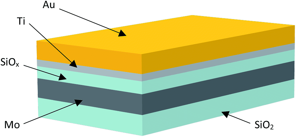 | ||
| Fig. 1 Schematic of the device structure. The SiO2 thermal oxide sits on top of a single crystal silicon wafer. Unless otherwise specified in the text, all layers above this are deposited by RF sputtering. | ||
Electrical characteristics were measured using a Keithley 4200SCS semiconductor characterisation system attached to a Signatone probe station. All measurements were obtained at room temperature in an open lab environment.
The preparation of the electron transparent lamella for transmission electron microscopy (TEM) was carried out using focused ion beam (FIB) preparation on a JEOL-JIB-4601F system with a final polishing voltage of 3 kV. Scanning transmission electron microscopy (STEM) and electron energy loss spectroscopy (EELS) analysis was carried out on an aberration corrected JEOL 2200FS (S)TEM system equipped with a JEOL in-column EELS filter. An acceleration voltage of 200 keV was used with a convergence semi-angle of 21.3 mrad and a collection semi-angle of 23.6 mrad.
Atomic force microscope (AFM) topography scans of samples were obtained using either a Bruker Icon AFM operating in non-contact mode, or a Nanosurf AFM operating in non-contact mode. To investigate the internal structure of conductive regions within the sputtered oxide we used a conductive AFM (C-AFM) tomography technique that uses a conductive diamond tip to measure 2D conductivity maps across the surface of the sample and then, by controlling the setpoint of the scan to increase the force exerted by the tip on the sample, removes layers of the oxide to take sequential 2D conductivity maps through the oxide bulk, from which we can construct a 3D map of variations in conductivity within the sputtered oxide.14,15
To further investigate the role of bottom electrode roughness on oxide structure and resistance switching properties, we used a fast electron beam lithography technique that allows us to make large area arrays of highly uniform nanometre-scale structures16 to fabricate samples with predefined nanopillar structures at the lower Mo electrode/SiOx interface. The Mo nanopillar array was fabricated on a Mo-coated SiO2/Si substrate. The substrate Mo layer was 100 nm thick and was deposited by electron beam evaporation to ensure a flat interface. For the electron beam lithography process, a PMMA layer was applied onto the Mo-coated substrate by spin-coating followed by baking to remove excess solvent. An array of nanosized holes was then patterned by using the fast electron beam lithography technique. Beam dwell time and energy were adjusted to define the final size of exposed spot, which in turn defined the size of the top of the holes. After developing the sample with MIBK:IPA solution, an array of nanoholes was formed in the PMMA layer. The sample was then transferred to a sputtering machine (Kurt Lesker PVD75) for Mo deposition (5 to 10 nm thick). After lift-off in acetone, a Mo nanopillar array was formed onto the Mo substrate. We prepared two different nanopillar samples: sample 1 had 5 nm tall, 70 nm diameter, Mo nanopillars in a square array with a pitch of 600 nm; sample 2 had 10 nm tall, 120 nm diameter, Mo nanopillars in a square array with a pitch of 300 nm. 35 nm of SiOx was deposited onto the array structures, followed by Ti/Au top electrodes, also sputtered, and electrode structures defined by standard photolithography.
Results and discussion
Fig. 2 shows a set of electroforming curves for three samples with varying bottom electrode roughness. The sample with the smoothest interface (rms roughness = 0.9 nm) has the highest electroforming voltages (−9 V), while that with the highest surface roughness (rms roughness = 1.5 nm) has the lowest electroforming voltage (−3.5 V). We note also that an increase in interface roughness correlates with a reduction in the spread of SET and RESET voltages between switching cycles. Thus, somewhat counter-intuitively, decreasing the quality of the electrode/oxide interface improves switching characteristics. Note also that the leakage currents pre-electroforming are considerably lower for the case of the flatter interface, implying that something in the structure of the samples with the rougher interfaces promotes the formation of conductive pathways through the oxide.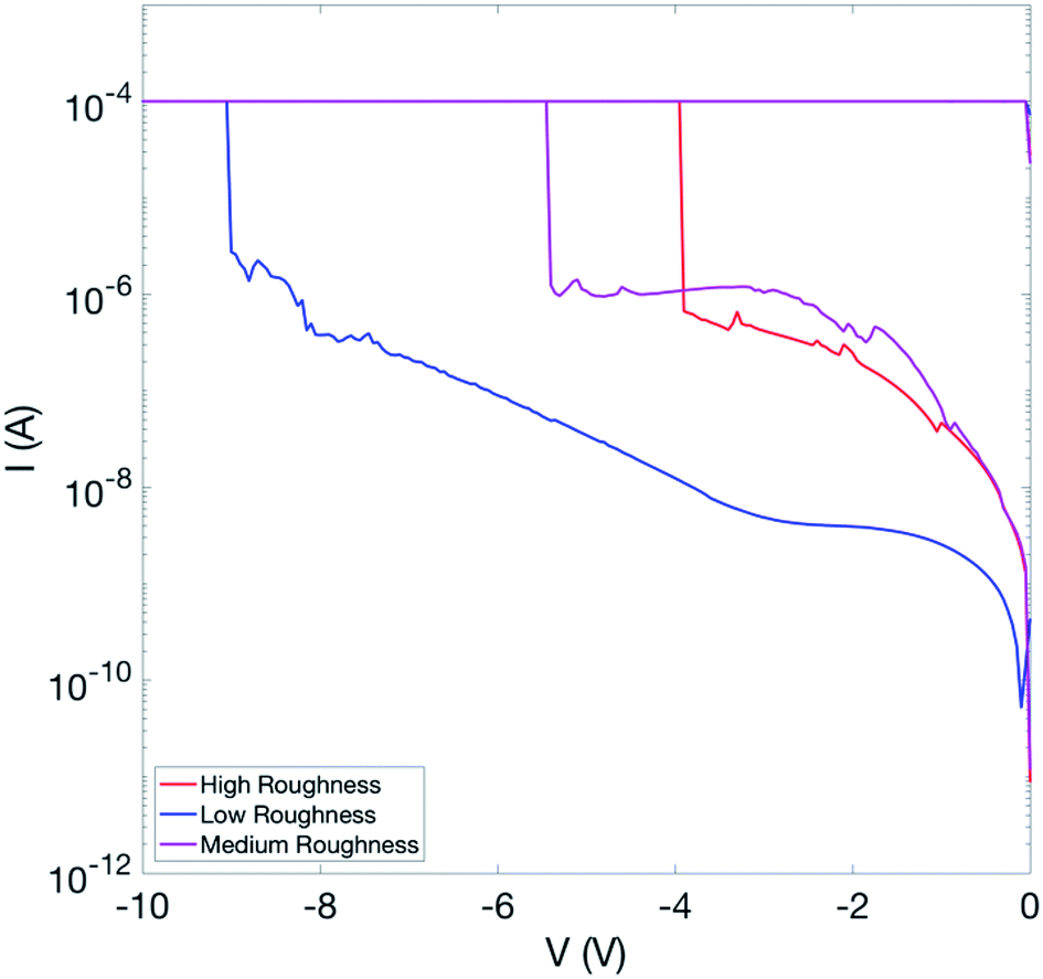 | ||
| Fig. 2 Typical electroforming I/V sweeps for samples fabricated with a range of bottom electrode interface roughnesses. High roughness = 1.5 nm rms; medium roughness = 1.1 nm rms; low roughness = 0.9 nm rms. | ||
Fig. 3 illustrates the cycle-to-cycle variability of two samples of different bottom electrode roughness. Fifteen switching cycles are shown for each. Note in particular the difference in the spread of SET voltages (negative bias). The sample with the rougher interface (rms roughness = 1.5 nm) shows a considerably smaller cycle-to-cycle variation than does the sample with the smoother interface (rms roughness = 1.1 nm).
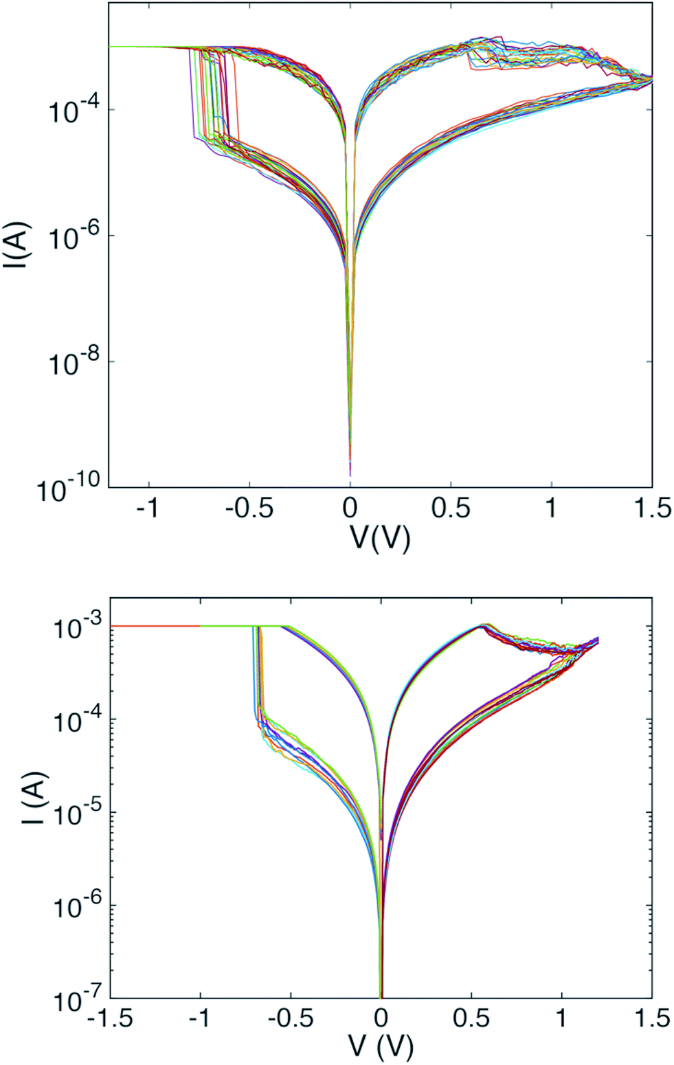 | ||
| Fig. 3 Top: 30 sequential current/voltage cycles of a Mo/SiOx/Ti/Au sample with a bottom electrode roughness of 1.1 nm rms. Bottom: a similar plot for a sample with a bottom electrode roughness of 1.5 nm rms. | ||
As mentioned previously, sputtering is recognised to produce thin films with a columnar internal structure.8 Atomic shadowing during the first stages of deposition can lead to the preferential growth of columns of material that merge during the deposition process. In the case of crystalline material, this results in polycrystalline growth with grain boundaries defined by the deposition parameters. In the case of amorphous material (such as our amorphous silicon oxide), column boundaries are more poorly defined, but can be thought of as defect-rich regions with a wide spread of bond angles, and may act as preferred sites for the inclusion of impurities and contaminants such as hydrogen or hydroxyl groups. Fig. 4 shows a TEM cross-section of a sputter-deposited sample in which the columnar structure of the bottom molybdenum electrode is clearly visible. It is worth noting that the surface features of the rough molybdenum surface appear to template the structure of the silicon oxide, and the features of the upper oxide interface mirror those of the lower interface.
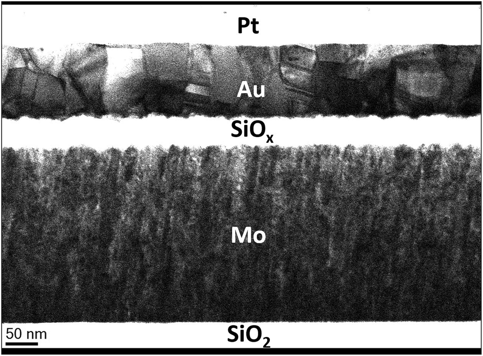 | ||
| Fig. 4 A TEM cross-sectional image of a Mo/SiOx/Ti/Au sample (Ti not labelled). The columnar structure of the bottom sputtered Mo electrode is clearly visible. Also noteworthy is the similarity in the profile of the top and bottom electrode interfaces. | ||
To confirm the presence of columnar structure within the oxide film, we performed scanning transmission electron microscopy (STEM) of an un-stressed sample. Fig. 5a shows this, with a contrast-enhanced image shown in Fig. 5b. Regions of alternating bright and dark contrast suggest the presence of columns and column edges, with column diameters of the order of tens of nanometres. The corresponding EELS silicon map (Fig. 5c) indicates depletion of silicon at what appear to be column edges, suggesting a lower density in these regions. This is confirmed by EELS oxygen mapping of similar regions (Fig. 5d), which indicates oxygen depletion at column boundaries.
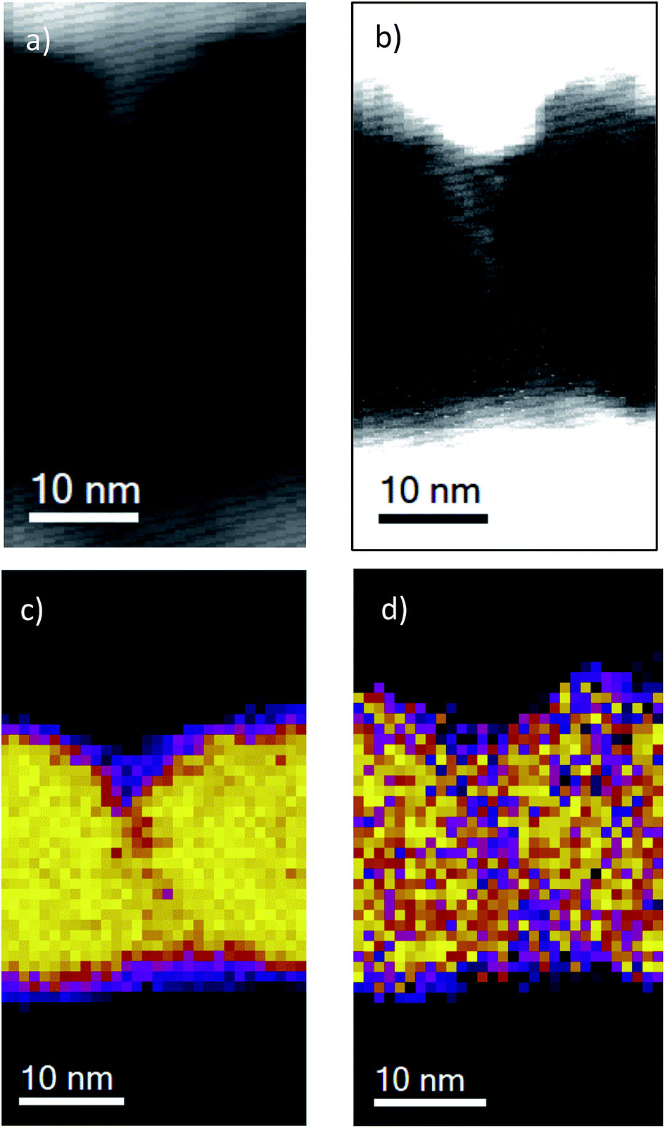 | ||
| Fig. 5 (a) TEM cross-sectional image of a sputtered MIM structure with Mo bottom electrode, 37 nm SiOx film, and Ti/Au top electrode. (b) Contrast enhanced image, showing column boundary in the centre of the image. (c) EELS map of silicon distribution. (d) EELS map of oxygen distribution. The column boundary appears to be a region of low density. | ||
In order to be confident that the initial current leakage through the oxide pre-electroforming was not due to the indiffusion of metal ions from the top electrode during deposition, we performed an EELS analysis of the distribution of titanium within a sample. This is shown in Fig. 6, which confirms that no titanium is present within the oxide bulk or at the column boundaries within the oxide.
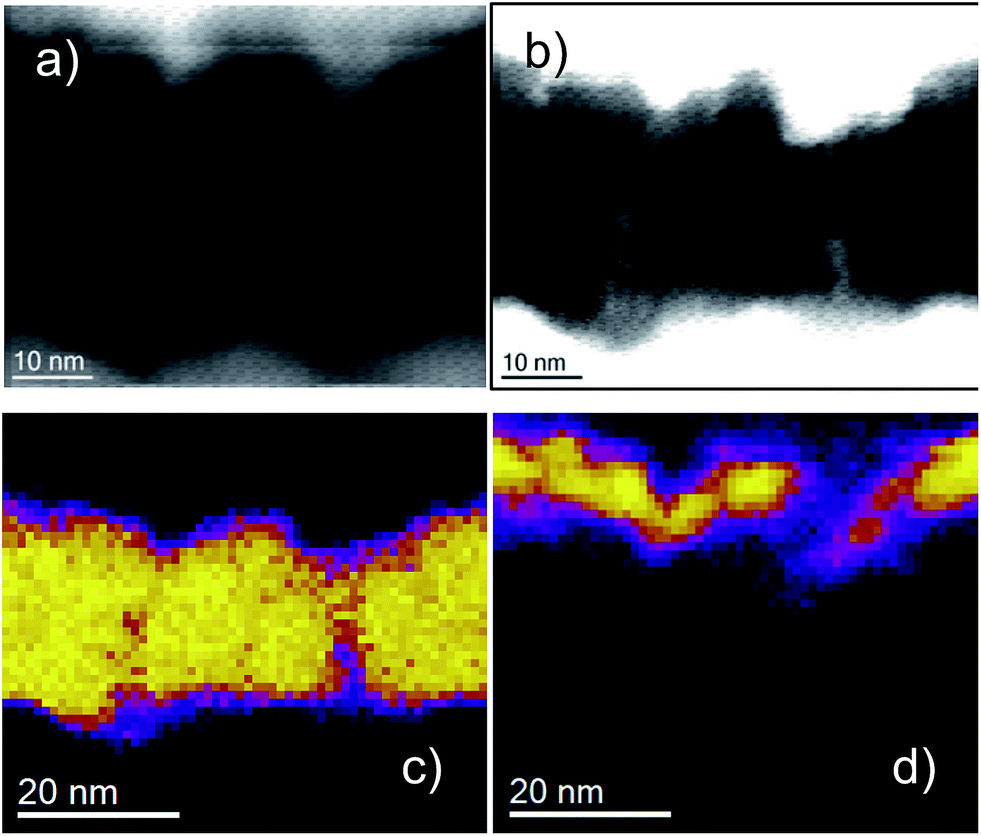 | ||
| Fig. 6 (a) TEM cross-sectional image of a sputtered MIM structure with Mo bottom electrode, 37 nm SiOx film, and Ti/Au top electrode. (b) Contrast enhanced image, showing column boundary in the centre of the image. (c) EELS map of silicon distribution. (d) EELS map of titanium distribution. There is no evidence of titanium within the oxide, or at the column boundaries. | ||
We note, interestingly, that our observation of increased stability of switching, as demonstrated by a reduction in the spread of switching voltages, is the opposite of that reported in other studies of the effect of interface roughness on resistance switching in oxides. Nandi et al., in ref. 17, for example, show that, in the case of oxide films deposited by atomic layer deposition (ALD), rougher interfaces produce less stable switching and reduced cycling endurance, although they also report a lowering of the electroforming voltage. Their finite element models suggest that high aspect ratio asperities (projections of the electrode material into the oxide) can result in local field enhancements of more than an order of magnitude. While this may be expected to have a major influence on switching characteristics, they conclude that the enhancement is moderated by the generation of defects within the oxide prior to electroforming. Thus, the oxide structure plays a crucial role in the switching process. It is worth noting in this context that ALD films tend to be highly uniform, in contrast to the columnar structure of sputtered films. This is also true of other deposition techniques that produce very uniform, smooth films, such as metal-organic chemical vapour deposition (MOCVD). We note, in support of this assertion, work by Gaillard et al.,18 demonstrating that, for MIM samples in which the lower TiN electrode is deposited by sputtering (and therefore consists of many grains and a rough top surface), if the oxide layer is deposited by MOCVD, the roughness of the top interface is much less than that of the bottom. The inference is that the deposition of a homogeneous oxide layer gradually reduces the roughness of the top interface to a value determined by the thickness of the oxide. Fig. 7 (taken from ref. 18) illustrates the effect using TEM cross-sections. This is in contrast to our results, which show that any differences in roughness between the two metal/oxide interfaces are rather small, and the bottom interface roughness templates the formation of columns in the oxide, which in turn template the roughness of the top interface (Fig. 4–6). To further illustrate this, Fig. 8 shows AFM topography scans of the surfaces of the top and bottom electrodes in one of our Mo/SiOx/Ti/Au structures, along with histograms of column diameters, and lognormal fits, for both. It is clear that the structure of the two interfaces is very similar, with mean column diameters of 71.36 nm and 78.36 nm for the bottom and top surfaces, respectively. This is suggestive that the roughness of the initial sputtered layer templates that of subsequent layers, and is responsible for the nature and scale of the microstructure within the oxide.
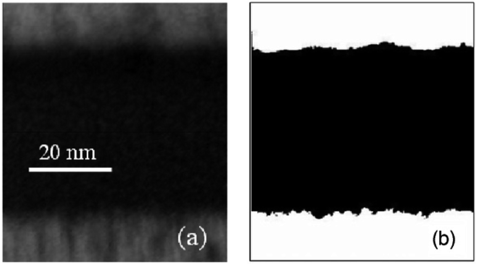 | ||
| Fig. 7 (a) TEM cross-sectional image of an MIM structure with sputtered tin bottom electrode, 45 nm MOCVD Ta2O5 film, and sputtered tin top electrode. (b) Contrast enhanced image, demonstrating the difference in roughness between the top and bottom electrode interfaces. Reproduced from ref. 18 with the permission of AIP Publishing. | ||
 | ||
| Fig. 8 (a) AFM topography scan of bottom electrode of Mo/SiOx/Ti/Au sample. (b) AFM topography scan of top electrode. (c) Histogram of distribution of column diameters for bottom electrode. (d) Histogram of distribution of column diameters for top electrode. | ||
We next investigated the samples with Mo nanopillars on the bottom Mo electrode/SiOx layer to determine the role of varying the SiOx layer thickness and possible field enhancement due to protrusions on the lower electrode interface. Fig. 9 shows typical electroforming curves for the two nanopillar samples, along with similar curves for samples with a smooth (evaporated) bottom electrode (surface roughness 0.65 nm rms) and a sputtered bottom electrode with a surface roughness of 1.5 nm rms. The first, perhaps surprising, observation is that both of the nanopillar samples exhibit considerably higher electroforming voltages than the sputtered Mo sample. The higher electroforming voltage for the evaporated Mo sample is expected, and consistent with our previous results,19 but it might be expected that introducing nanopillar structures onto the bottom electrode would reduce the electroforming voltage through two effects: a thinning of the SiOx layer above the nanopillar, and electric field enhancement at the tips of the pillars or at the edges of the pillar tops. The fact that this is clearly not the case suggests an alternative explanation.
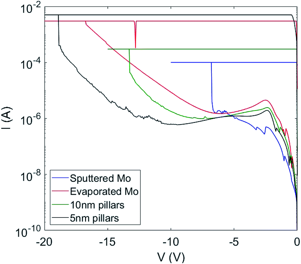 | ||
| Fig. 9 Electroforming curves from samples with differently structured bottom electrode/SiOx interfaces. Evaporated Mo has the smoothest interface, followed by the sputtered layer. The green line shows results from a sample with 10 nm high Mo pillars on an evaporated bottom Mo electrode (120 nm radius, 300 nm spacing). The black line shows results from a sample with 5 nm high Mo pillars on an evaporated bottom Mo electrode (70 nm radius, 600 nm spacing). In all cases the SiOx layer was 38 nm thick. | ||
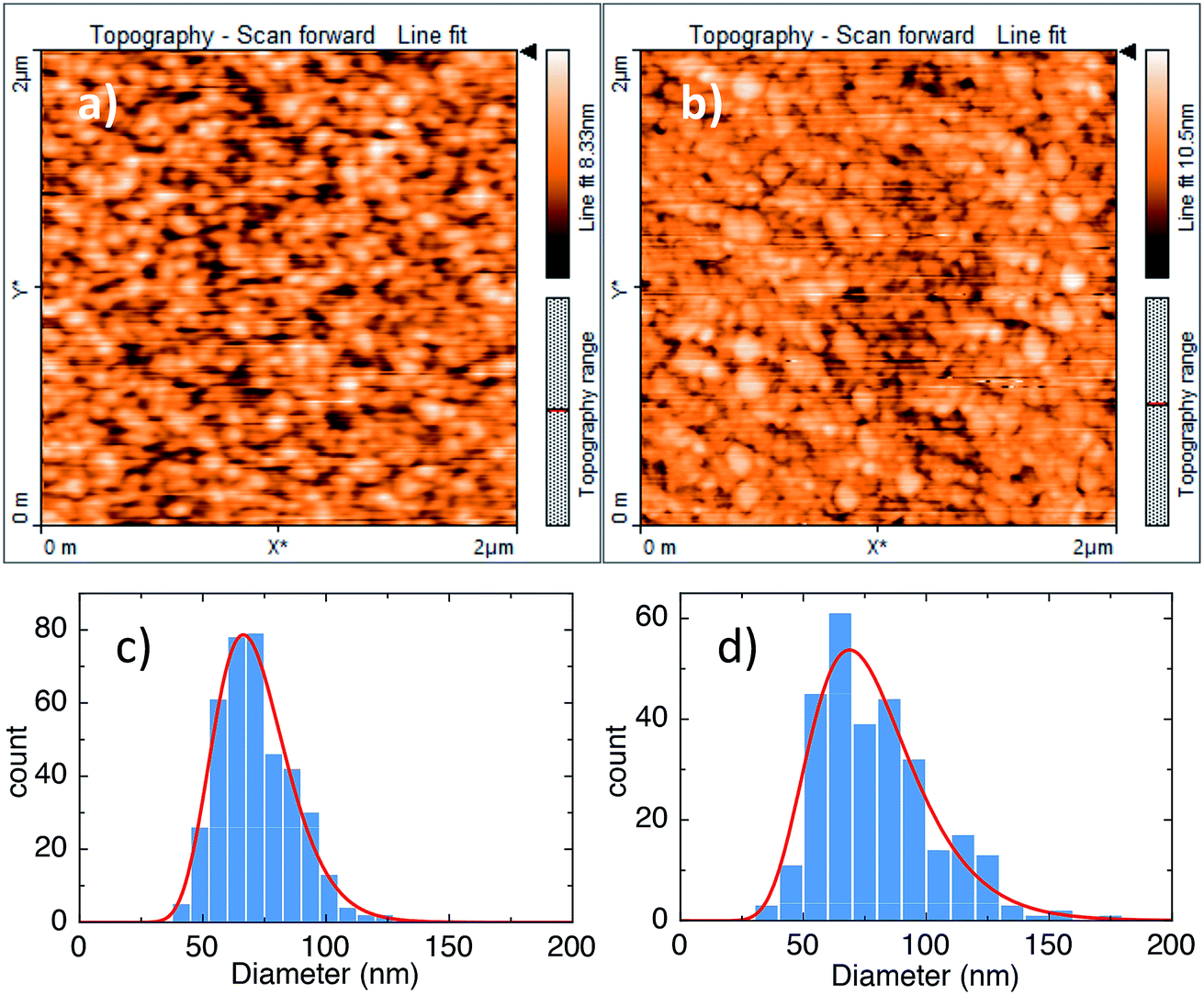
Fig. 10 shows AFM topography scans of the evaporated Mo layer, and of the two samples with Mo nanopillars. Also included for comparison is a scan of the surface of the SiO2 substrate onto which the Mo has been evaporated. The substrate has a surface roughness of 0.18 nm rms, while that of the evaporated Mo layer is 0.65 nm rms, confirming that evaporated layers have a significantly lower surface roughness than those that have been sputtered. From these results we note that the tops of the nanopillar structures are not flat, partly because the pillars were deposited by sputtering, and partly because of shadowing effects during deposition into the nanoholes or an effect of the removal of the PMMA layer. Whatever the cause, the uneven top surfaces of the nanopillars can be expected to generate electric field enhancement within the switching layer under bias. Nevertheless, these samples exhibit the highest electroforming voltages. We can conclude from this that it is not primarily electric field enhancement that drives the lowering of electroforming voltages, but the presence of microstructure in the form of column boundaries in the oxide, templated by the sputtered bottom electrode.
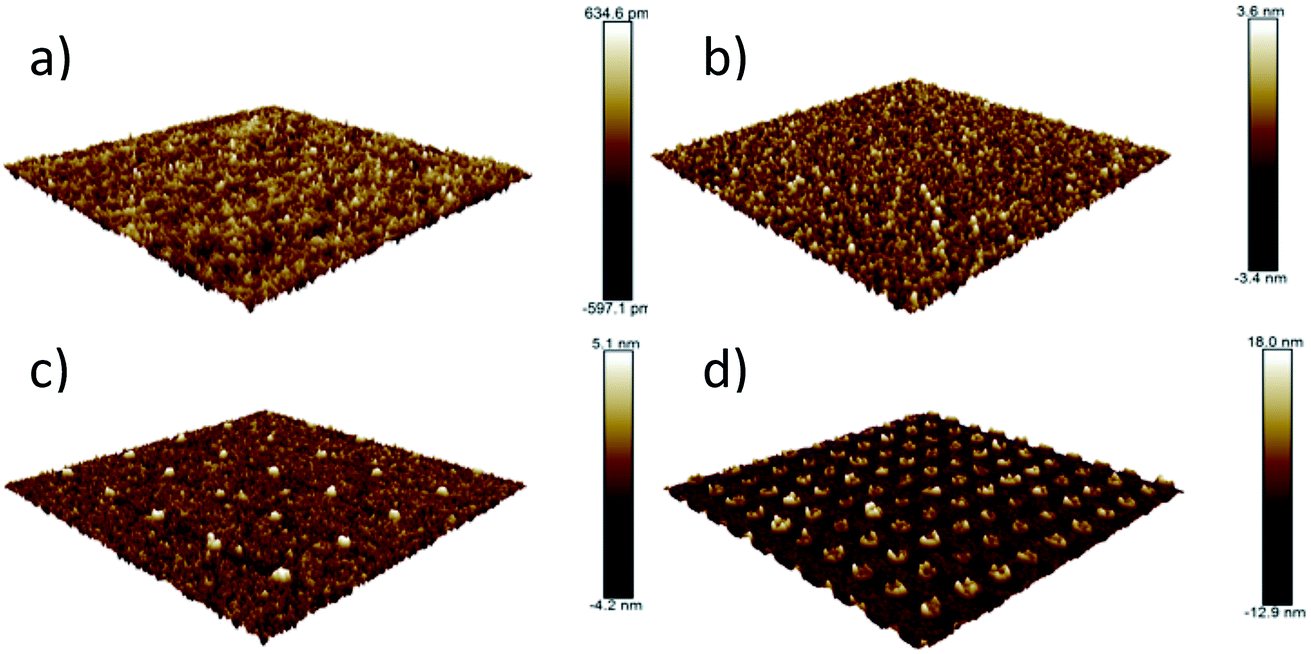 | ||
| Fig. 10 AFM topography scans of: (a) SiO2 surface onto which the bottom Mo electrode was evaporated; (b) surface of evaporated Mo electrode; (c) evaporated Mo electrode with 5 nm tall Mo nanopillars; (d) evaporated Mo electrode with 10 nm tall Mo nanopillars. | ||
Finally, to further demonstrate the presence of columnar structure within the sputtered oxide, Fig. 11 shows 3D conductive AFM tomography results from an electroformed SiOx layer that has been deposited onto a sputtered TiN bottom electrode. The centre of the image shows that several conductive filaments have coalesced during electroforming to form a compound filament several hundred nanometres in diameter connecting the top and bottom electrodes. What is more relevant to our discussion is the observation that regions of enhanced conductivity within the rest of the oxide reveal the internal columnar structure of the sputtered material. We note that these results are consistent with our measurements presented elsewhere of large-scale oxygen movement in stressed oxides,7 and with the internal oxide structure shown in Fig. 5 and 6. Taken together, these results suggest that the internal column boundaries provide sites for the aggregation of defects that act as precursors for the formation of oxygen vacancies, aggregates of which are responsible for the formation of conductive pathways through the oxide. The vertical boundaries further provide channels for the movement of oxygen under electrical bias, and hence can act as templates for the formation of conductive filaments responsible for resistance switching. Oxide microstructure is therefore a critical determinant of the electrical behaviour of amorphous oxides.
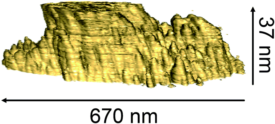 | ||
| Fig. 11 3D C-AFM tomographic image of the internal microstructure of an SiOx layer. Surrounding the composite conductive filament formed by the coalescence of several smaller filaments are regions of enhanced conductivity that reveal the internal columnar structure of the oxide. | ||
Conclusions
We have reported the intimate dependence of intrinsic resistance switching on microstructure in amorphous silicon oxide. Even in amorphous material, the presence of extended defects in the form of column boundaries promotes the formation of conductive filaments of oxygen vacancies by offering predetermined distributions of defects and channels for oxygen movement. Column boundaries can be effectively generated by providing a rough interface between the bottom electrode and switching layer. While increased interface roughness results in electric field enhancement at regions of particularly pronounced roughness, this effect appears to be secondary to the control of columnar structure thanks to a roughness templating effect during sputter growth. Control over the microstructure of oxides at the scale of tens of nanometres offers the opportunity to tailor resistance switching parameters such as electroforming voltage and distributions of switching voltages. Column boundaries within amorphous oxides can be initiated by deposition or processing techniques that generate preferential pathways for the formation of conductive filaments. Our results suggest that this has the welcome effect of both reducing electroforming voltages and greatly reducing the cycle-to-cycle variability of switching voltages.Conflicts of interest
The authors confirm that there are no conflicts to declare.Acknowledgements
The authors gratefully acknowledge funding provided by the Engineering and Physical Sciences Research Council and by the Leverhulme Trust to support the research presented here.References
- R. W. Brander, D. R. Lamb and P. C. Rundle, Br. J. Appl. Phys., 1967, 18, 23 CrossRef CAS.
- G. Dearnaley, A. M. Stoneham and D. V. Morgan, Rep. Prog. Phys., 1970, 33, 1129 CrossRef.
- A. M. Stoneham, J. L. Gavartin and A. L. Shluger, J. Phys.: Condens. Matter, 2005, 17, S2027 CrossRef CAS.
- J. Yao, Z. Sun, L. Zhong, D. Natelson and J. M. Tour, Nano Lett., 2010, 10, 4105 CrossRef CAS.
- A. Mehonic, S. Cueff, M. Wojdak, S. Hudziak, O. Jambois, C. Labbé, B. Garrido, R. Rizk and A. J. Kenyon, J. Appl. Phys., 2012, 111, 074507 CrossRef.
- C. Li, L. L. Han, H. Jiang, M. H. Jang, P. Lin, Q. Wu, M. Barnell, J. J. Yang, H. L. L. Xin and Q. F. Xia, Nat. Commun., 2017, 8, 15666 CrossRef CAS.
- A. Mehonic, M. Buckwell, L. Montesi, M. S. Munde, D. Gao, S. Hudziak, R. J. Chater, S. Fearn, D. McPhail, M. Bosman, A. L. Shluger and A. J. Kenyon, Adv. Mater., 2016, 28, 7486 CrossRef CAS.
- J. A. Thornton, J. Vac. Sci. Technol., 1974, 11, 666 CrossRef CAS.
- D. S. Jeong, H. Schroeder, U. Breuer and R. Waser, J. Appl. Phys., 2008, 104, 123716 CrossRef.
- A. Mehonic and A. J. Kenyon, in Defects at Oxide Surfaces, ed. J. Jupile and G. Thornton, Springer International Publishing, Basel, Switzerland, 2015, pp. 401–428 Search PubMed.
- D. Ielmini, Semicond. Sci. Technol., 2016, 31, 063002 CrossRef.
- A. Mehonic, M. S. Munde, W. H. Ng, M. Buckwell, L. Montesi, M. Bosman, A. L. Shluger and A. J. Kenyon, Microelectron. Eng., 2017, 178, 97 CrossRef.
- J. J. Yang, M. X. Zhang, J. P. Strachan, F. Miao, M. D. Pickett, R. D. Kelley, G. Medeiros-Ribeiro and R. S. Williams, Appl. Phys. Lett., 2010, 97, 232102 CrossRef.
- U. Celano, L. Goux, A. Belmonte, K. Opsomer, A. Franquet, A. Schulze, C. Detavernier, O. Richard, H. Bender, M. Jurczak and W. Vandervorst, Nano Lett., 2014, 14, 2401 CrossRef CAS PubMed.
- M. Buckwell, L. Montesi, S. Hudziak, A. Mehonic and A. J. Kenyon, Nanoscale, 2015, 7, 18030 RSC.
- W. H. Ng, Y. Lu, H. Liu, C. J. Carmalt, I. P. Parkin and A. J. Kenyon, Sci. Rep., 2018, 8, 3544 CrossRef.
- S. K. Nandi, X. Liu, D. K. Venkatachalam and R. G. Elliman, Phys Rev Appl, 2015, 4, 064010 CrossRef.
- N. Gaillard, L. Pinzelli, M. Gros-Jean and A. Bseisy, Appl. Phys. Lett., 2006, 89, 133506 CrossRef.
- M. S. Munde, A. Mehonic, W. H. Ng, M. Buckwell, L. Montesi, M. Bosman, A. L. Shluger and A. J. Kenyon, Sci. Rep., 2017, 7, 9274 CrossRef CAS.
| This journal is © The Royal Society of Chemistry 2019 |