 Open Access Article
 This Open Access Article is licensed under a
 Creative Commons Attribution 3.0 Unported Licence
Impact of oxide and electrode materials on the switching characteristics of oxide ReRAM devices
Elia
Ambrosi
 ,
Alessandro
Bricalli
,
Mario
Laudato
and
Daniele
Ielmini
*
,
Alessandro
Bricalli
,
Mario
Laudato
and
Daniele
Ielmini
*
Dipartimento di Elettronica, Informazione e Bioingegneria, Politecnico di Milano, Piazza L. da Vinci 32, 20133 Milano, Italy. E-mail: daniele.ielmini@polimi.it
First published on 18th September 2018
Abstract
Resistive switching random-access memory (ReRAM) is one of the most promising technologies for non-volatile memories. Thanks to the low power and high speed operation, the high density CMOS-compatible integration, and the high cycling endurance, the ReRAM technology is becoming a strong candidate for high-density storage arrays and novel in-memory computing systems. However, ReRAM suffers from cycle-to-cycle switching variability and noise-induced resistance fluctuations, leading to insufficient read margin between the programmed resistive states. To overcome the existing challenges, a deep understanding of the roles of the ReRAM materials in the device characteristics is essential. To better understand the role of the switching layer material in controlling ReRAM performance and reliability, this work compares SiOx- and HfO2-based ReRAM at fixed geometry and electrode materials. Ti/HfO2/C and Ti/SiOx/C devices are compared from the point of view of the forming process, switching characteristics, resistance variability, and temperature stability of the programmed states. The results show clear similarities for the two different oxides, including a similar resistance window and stability at high temperatures, thus suggesting a common nature of the switching mechanism, highlighting the importance of the electrodes. On the other hand, the oxide materials play a clear role in the forming, breakdown, and variability characteristics. The discrimination between the role of the oxide and the electrode materials in the ReRAM allows ReRAM optimization via materials engineering to be better explored for future memory and computing applications.
1 Introduction
In recent years, resistive switching memory (ReRAM) devices have emerged as strong candidates for next generation high-density storage technologies.1–3 The resistance switching mechanism enables not only high-density non-volatile memory with high speed, high endurance, and low power, but can also be exploited for implementing novel computing paradigms such as in-memory computing and neuromorphic computing.4–6 Currently, ReRAM technologies are facing significant challenges due to switching variability and resistance fluctuations, which require major breakthroughs at the levels of materials engineering and device physics.7–9In previous works, we proposed a silicon oxide-based ReRAM, in which an ultra-thin layer of SiOx is sandwiched between an inert carbon bottom electrode (BE) and an active titanium top electrode (TE).10 Electrical switching between a high-resistance state (HRS) and a low-resistance state (LRS) was attributed to the oxidation of titanium in the TE and migration of Ti ions into the solid electrolyte, where they react to form a Ti-rich conductive filament (CF). This type of switching is equivalent to the well-known conductive bridge RAM (CBRAM), or electrical metallization cell (EMC). The adoption of a TE made of Cu and Ag was shown to lead to volatile switching, which might be applicable for selector devices in high density crosspoint arrays11 and synaptic devices.12
In the static regime, SiOx-based ReRAM shows an outstanding resistance window exceeding 104. On the other hand, a ratio of about 10 is typically found in HfO2-based ReRAM, where switching is generally assumed to be due to the oxidation/reduction of metallic elements, known as the valence change memory (VCM) mechanism.13 The larger resistance window of the SiOx ReRAM is in agreement with previous studies which attribute a larger window to CBRAM-type devices.14 A high resistance window is essential in ReRAM to allow for sufficient read margin between the HRS and the LRS, ensuring a sufficient immunity from post-programming fluctuations of resistance.9 SiOx ReRAM has also shown a relatively low variability, an excellent cycling endurance, and an outstanding stability at elevated temperature,10 compared with HfO2 ReRAM.15,16 To enable a high device reliability and a deeper understanding of the materials parameters controlling the resistance window, ReRAM materials should be compared at fixed geometry and top/bottom electrode types.
In this work, we compare SiOx-based ReRAM and HfO2-based ReRAM on the same test vehicle, which is a one-transistor/one-resistor (1T1R) structure which enables a tight control of the programming current, namely the compliance current IC. A comprehensive comparison is conducted, covering the forming operation, the switching characteristics, and the retention behavior at elevated temperature. We also investigate cycle-to-cycle variability by means of the relative standard deviation, namely the ratio between the standard deviation σR and the resistance R, which is the standard metric for stochastic variation of programmed states in ReRAM. Our results indicate that the SiOx and HfO2 ReRAM show remarkably similar device properties when compared on the same test vehicle. Similar performance includes the large resistance window and the good retention at elevated temperature. This performance similarity suggests that the ReRAM behavior is mostly dictated by the Ti TE and its migration controlling the filamentary switching in the two devices. On the other hand, the forming, breakdown and variability characteristics show remarkable dependence on the oxide material, which enables discrimination between the role of the oxide and of the electrode materials in the ReRAM switching mechanism.
2 Device structures
Fig. 1 illustrates the two ReRAM structures studied in this work, namely the SiOx-based ReRAM (a) and the HfO2-based ReRAM (b). Both devices were deposited on pre-patterned substrates with metal-oxide semiconductor (MOS) field-effect transistors (FETs) to enable the fabrication of 1T1R structures. After a 300 °C vacuum pre-processing of the substrates, a thin dielectric film was deposited by electron-beam evaporation from silicon monoxide (SiOx, x ≈ 1) or hafnium dioxide (HfO2) solid targets on top of a graphitic carbon bottom electrode (BE) of area 70 × 70 nm2.10 The Ti TE was deposited on top of the oxide layer without breaking the vacuum from the previous oxide deposition. The Ti TE had a thickness of 50 nm. A tungsten plug connects the BE to the drain of the FET to enable an integrated 1T1R structure. The HfO2 film was deposited with a thickness of tox = 5 nm or tox = 10 nm, whereas the SiOx film thickness was tox = 5 nm.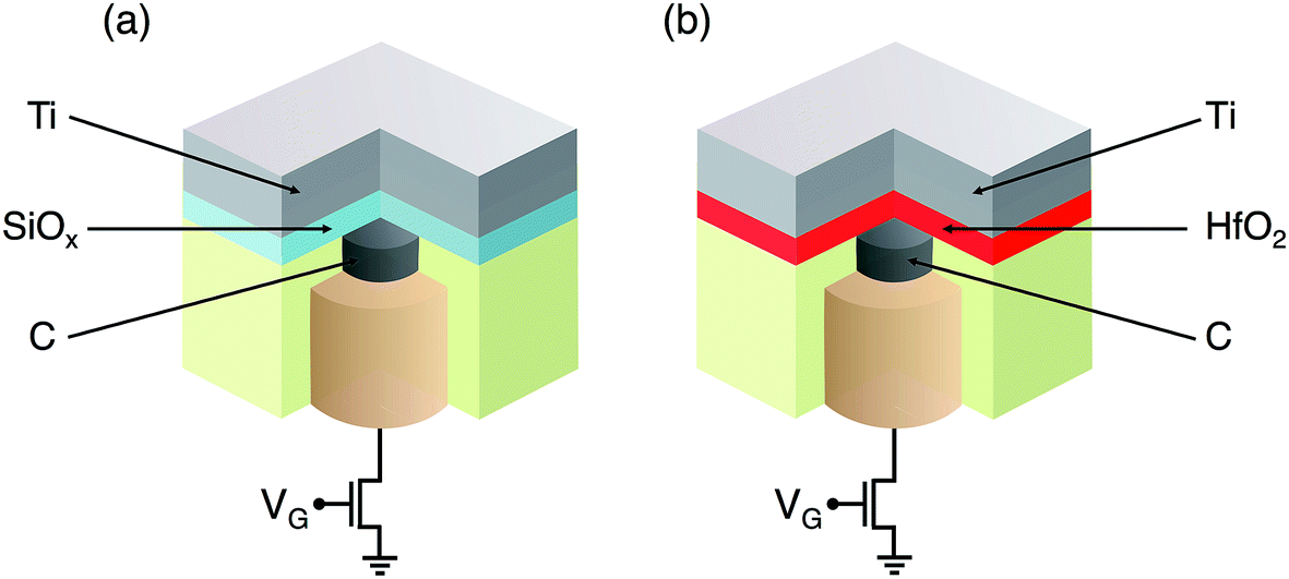 | ||
| Fig. 1 Schematic illustration of the (a) SiOx-based, and (b) HfO2-based ReRAM devices. The dielectric switching layer is deposited on top of a graphitic C bottom electrode. The Ti top electrode serves as the active electrode supplying Ti impurity defects for the filament formation. | ||
After the fabrication process, the devices were electrically characterized in a probe station by means of a Keysight B1500A semiconductor parameter analyzer.
3 Forming and switching characteristics
3.1 Forming
Fig. 2(a) shows the I–V curves measured on the pristine cell for 30 devices for tox = 5 nm. The voltage was applied to the TE and increased at a rate of about 1 V s−1. The gate of the FET in the 1T1R structure was biased with a voltage VG in the range between 1 V and 1.6 V, corresponding to a compliance current IC between 1 and 70 μA, while the source was grounded. | ||
| Fig. 2 (a) I–V characteristics of the forming process in the HfO2 and SiOx stacks of thickness tox = 5 nm. (b) Experimental cumulative probability of the forming voltages VFORM in different devices. (c) Experimental cumulative probability of the leakage current ILEAK extracted at fixed voltage V = 2.5 V from the I–V curves, in different devices. The two stacks show comparable leakage currents, slightly higher in the HfO2 device, while the forming voltage is higher in SiOx. | ||
Initially, the pristine device shows very low leakage current, limited by the instrument resolution for a TE voltage below 1.5 V. The current increases for increasing positive voltage, as a result of Poole–Frenkel conduction at localized states. Forming appears as a sudden step in the I–V curves, at a characteristic voltage VFORM, triggering a soft breakdown which brings the device in the LRS. The forming operation marks the initial formation of a CF, the size of which is controlled by the maximum current IC through the device, which also prevents the irreversible breakdown of the ReRAM device upon forming.
From the I–V curves in Fig. 2(a), one can notice a large difference in VFORM, which is about ≈4 V for HfO2 and ≈7.5 V for SiOx. Fig. 2(b) shows the cumulative distributions of VFORM for the ReRAM devices, which also reveal a higher distribution spread for HfO2 compared to SiOx. On the other hand, the leakage current ILEAK before forming is comparable in the two dielectric materials, as confirmed by the probability distributions in Fig. 2(c) showing ILEAK at V = 2.5 V. The leakage current shows a larger distribution spread and higher noise in HfO2, possibly related to the higher instability of defects such as oxygen vacancies compared to SiOx. The lower VFORM in HfO2 results in a lower forming current, which is about 1 nA in HfO2 compared to 10 to 100 nA in SiOx. Such a result may be due to a smaller energy barrier for defect migration in HfO2, compared to SiOx, which is also supported by the higher current noise and the lower breakdown voltage (see Sec. 4.1).
3.2 Switching characteristics
Fig. 3 shows our interpretation of the switching mechanism in a filamentary bipolar ReRAM. The forming operation results in the formation of a continuous defect-rich conductive filament (CF) of diameter ϕ connecting the two electrodes. This corresponds to the low resistance state (LRS) of the memory device depicted in Fig. 3(a). During the reset operation, the CF is disrupted thus resulting in a transition to the high resistance state (HRS) in Fig. 3(b). During the reset transition, initiated by the application of a negative voltage to the TE, positively-ionized defects (Ti impurities and/or oxygen vacancies) migrate towards the TE in response to the applied field, thus leaving behind a highly-resistive depleted gap of length Δ.17 The application of a positive voltage to the TE induces the migration of defects from the TE into the depleted gap, leading to the reconnection of the CF. | ||
| Fig. 3 Schematic representation of the set/reset operations in the ReRAM device. (a) In the low resistance state (LRS) a continuous conductive filament (CF) connects the top electrode (TE) and the bottom electrode (BE). The reset operation causes the disconnection of the CF and the consequent transition to the high resistance state (HRS) (b). The set operation brings the device back to the LRS. | ||
Fig. 4 shows the measured I–V curves for 50 cycles for HfO2 with tox = 10 nm (a) and SiOx with tox = 5 nm (b). After the forming process the ReRAM device can be brought back to the HRS by the application of a negative voltage to the TE, inducing a reset transition. When the negative voltage exceeds Vreset a gradual decrease of current takes place, due to the field-induced migration and consequent disruption of the CF. The HRS resistance is about 108 Ω at the read voltage Vread = −0.5 V. The application of a positive voltage induces the set process in the ReRAM leading to the LRS at the characteristic set voltage Vset. The abrupt nature of the set transition can be explained by a positive feedback effect, where the electric field induces defect migration toward the depleted gap, which in turn causes an increase of the electric field and temperature by Joule heating. This positive feedback results in a self-accelerated dynamics of the CF growth at the origin of the abrupt set transition.13,18 During the set process the gate of the transistor is biased to VG = 1.6 V to limit the maximum current to IC = 80 μA. The current limitation serves as an external negative feedback mechanism to prevent irreversible breakdown of the device. Moreover, the maximum current through the device controls the size of the CF,19 yielding an inverse proportionality between compliance current and LRS resistance R ∝ 1/IC. The stop voltage was the same in the two sets of experiments, namely Vstop = −3.5 V.
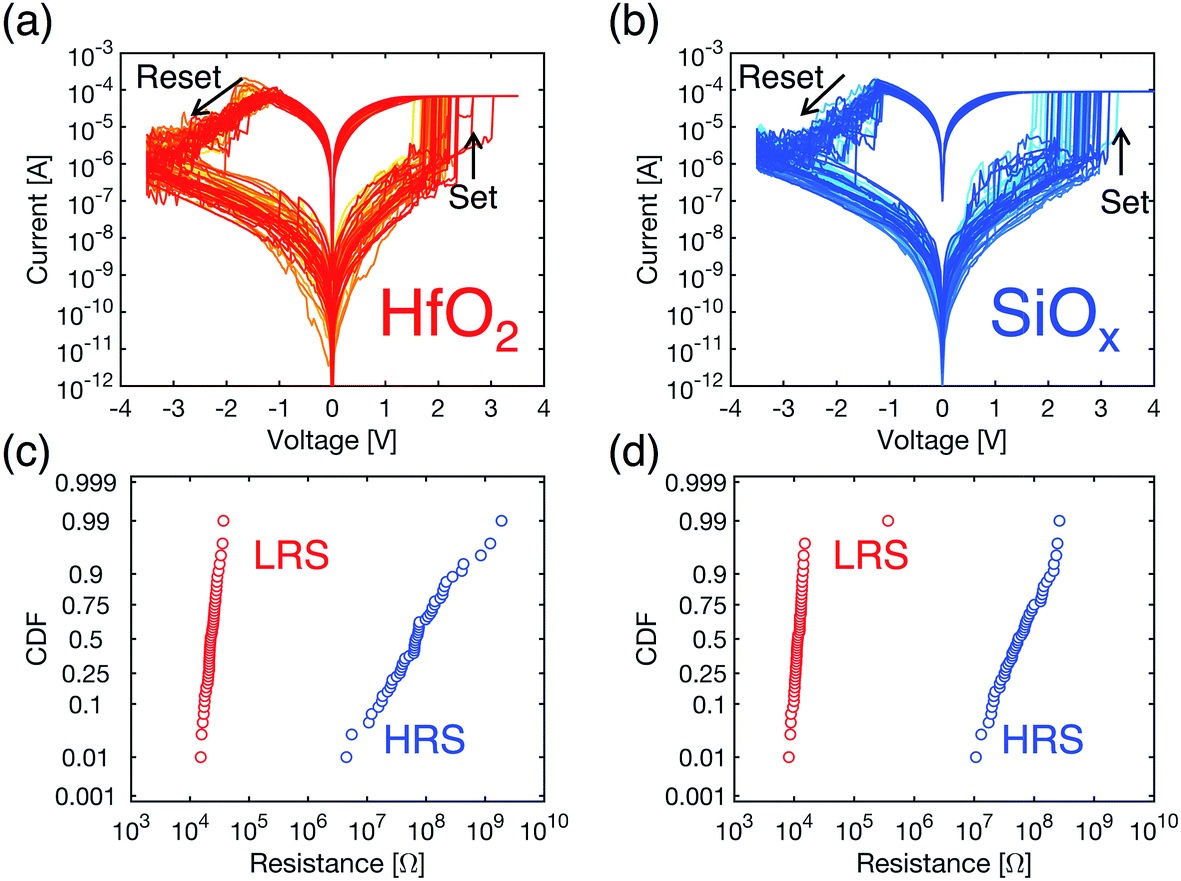 | ||
| Fig. 4 Measured I–V curves for HfO2 (a) and for SiOx (b), and the corresponding distributions of resistance for the HRS and LRS (c, d). The compliance current was IC = 80 μA and the stop voltage was Vstop = −3.5 V. The resistance window is about 5000 in both cases, which supports a similar mechanism for switching in the two stacks. | ||
HfO2 and SiOx ReRAM characteristics show comparable switching behavior, indicating an average resistance window of 5 × 10³ in SiOx and 3 × 10³ in HfO2. A significant difference lies in the HRS variability, which is significantly higher in HfO2. This is further confirmed by the cumulative probability distributions of the resistance values measured at −0.5 V in Fig. 4(c) and (d) for HfO2 and SiOx, respectively. The resulting relative standard deviation of the HRS is σR/R ≈ 1 in the SiOx stack and σR/R ≈ 5 in HfO2. The larger HRS variability can be interpreted by a higher distribution of energy barriers for defect migration controlling the variation in the reset characteristics.8
The nature of resistive switching in SiOx is attributed to the migration of Ti cations from the TE into the switching layer, resulting in the formation of a Ti-rich CF,10 and/or to the migration of oxygen vacancies leading to silicon nanoinclusions constituting the CF.20 Resistive switching in HfO2 is typically attributed to oxygen vacancies, although migration of metallic cations from the active TE into the metal oxide has been postulated19 and experimentally demonstrated.21 However, the similarity of the switching characteristics in Fig. 4 in terms of shape of the I–V curve and resistance window suggests that the SiOx and HfO2 share a similar microscopic switching mechanism, which might be the migration of Ti from the TE electrode controlling the CF formation and disruption.
3.3 Impact of Vstop
During the reset process, the resistance of the ReRAM gradually increases with the applied negative voltage, as a result of the inherent negative feedback mechanism regulating the growth of the depleted gap.13,18 As a consequence, the maximum applied negative voltage Vstop controls the length of the depleted gap and thus plays a key role to control the HRS and thus the resistance window.The dependence of the HRS on Vstop was studied for tox = 5 nm and tox = 10 nm HfO2 and for the reference SiOx stack, and the results are reported in Fig. 5. Fig. 5 shows the measured I–V curves (a) and the resistance values for the LRS and HRS as a function of Vstop (b) for a HfO2 ReRAM with tox = 5 nm. Vstop was changed every five set–reset cycles from Vstop = −2.2 V to −3.4 V, while the compliance current was kept constant at IC = 50 μA. The results show that Vstop controls the HRS, hence the resistance window, while the LRS remains almost unaffected by Vstop. The HRS increases exponentially at increasing Vstop with a slope of 1.2 dec V−1. For Vstop = −3.4 V, the device undergoes breakdown under negative voltage, which was already shown to control endurance lifetime under pulsed set/reset cycling experiments.15 In the breakdown phenomenon, the current suddenly increases, usually resulting in a LRS with an extremely low resistance due to the IC not being directly limited by the series FET. More results about the negative-voltage breakdown will be given in Sec. 4.1.
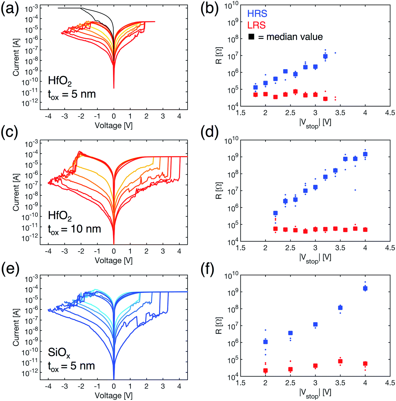 | ||
| Fig. 5 Measured I–V curves and resistance values as a function of |Vstop|, for (a, b) 5 nm HfO2, (c, d) 10 nm HfO2, and (e, f) 5 nm SiOx. |Vstop| was changed on the same device, starting from low |Vstop| values. IC was kept constant at IC = 50 μA. | ||
Fig. 5 also shows the I–V curves (c) and the resistance values (d) for the HfO2 ReRAM with tox = 10 nm. No breakdown phenomenon is seen at negative voltage, even up to Vstop = −4 V, possibly thanks to the thicker oxide layer limiting the electric field within the oxide layer. The resistance window could be effectively increased to more than 104 at the highest Vstop.
Data for SiOx (tox = 5 nm) are also shown for comparison, including I–V curves (e) and resistance values (f). The resistance values are similar to the HfO2 device with tox = 10 nm, except for the tighter control of the HRS which is promising for multilevel operation of the memory. Also notice that Vset increases in general with the Vstop adopted in the previous reset cycle, paralleling the increase of the HRS resistance. Excessive values of Vset might be detrimental for ReRAM operation, which relies on low voltage operation, which suggests that a tight control of the HRS and the associated Vset is essential in ReRAM devices.
3.4 Switching variability
Statistical variability of ReRAM parameters, including the HRS/LRS resistance, Vset and Vreset, is crucial for the memory performance and the read window margin. To study the switching variability in the two materials, we collected cycle-to-cycle distributions of the HRS and LRS and evaluated the corresponding standard deviation σR and the average resistance R for each distribution at various conditions of IC and Vstop. Fig. 6 shows the relative standard deviation σR/R as a function of R for the HfO2 ReRAM (tox = 10 nm) and the SiOx ReRAM (tox = 5 nm).22 In the figure, LRS data were obtained at variable IC while HRS data were obtained at variable Vstop. The LRS variation shows similar behavior in the HfO2 and SiOx ReRAMs, indicating a linear increase of σR/R with R. The latter is consistent with a variability model based on the stochastic variation of the CF shape from cycle to cycle.23 A lower LRS variability was found in HfO2 for relatively large resistance values (R ≈ 105 Ω), namely for low IC. | ||
| Fig. 6 Relative resistance spread σR/R as a function of the resistance R for 10 nm thick HfO2 compared to SiOx data in ref. 22. The data show comparable LRS variability, while the HRS is much more stable in SiOx, showing a larger window for the same relative spread, and a weaker dependence of σR/R on R. | ||
HRS variation shows a slightly different behavior in the two materials, with HfO2 indicating an increase of σR/R with R approximately given by R0.5, in agreement with previous variability models based on the Poissonian statistics controlling the number of defects in the depleted gap.7,8 On the other hand, SiOx ReRAM shows an almost constant σR/R ≈ 1 even for the highest R values around 1 GΩ. These data thus support the superior performance of SiOx ReRAM in terms of cycle-to-cycle variability, which plays a key role in the ReRAM memory operation and yield.
4 Reliability study
4.1 DC breakdown
Fig. 7(a) shows I–V characteristics of HfO2 ReRAM devices with tox = 5 nm for negative voltage, indicating the typical reset process of decreasing current, and the anomalous breakdown process where the current suddenly increases at a stochastic breakdown voltage VBD. Breakdown occurs during the negative voltage sweep and leads to an LRS with extremely low resistance. Similar breakdown phenomena were observed in 1T1R structures during pulsed cycling and attributed to rupture of the BE interface and a consequent defect injection from the BE.15 Negative-set cycles are generally destructive events, causing the failure of the memory device. In fact, during the application of negative voltages the gate of the integrated series transistor is generally biased to a relatively large voltage to minimize the voltage drop across the series transistor. This results in an overgrowth of the CF during negative-set, leading to a stuck-set state. To prevent irreversible breakdown in Fig. 7(a), the current meter was set to force a compliance current of 1 mA, thus much larger than the typical operating currents Ireset ≈ IC of about 80 μA. | ||
| Fig. 7 (a) Typical failure mechanism in HfO2 ReRAM devices is by negative-set breakdown. (b) SiOx devices (tox = 5 nm) do not show negative-set up to very large negative voltages. | ||
While HfO2 ReRAM with tox = 5 nm systematically shows breakdown, the same is not observed in the SiOx ReRAM with the same oxide thickness, even when relatively large negative voltages are applied, e.g., Vstop = −10 V in Fig. 7(b). This might be attributed to the higher energy barrier for defect migration in the SiOx layer, compared to HfO2, which is also consistent with the higher VFORM of SiOx in Fig. 2.
4.2 Retention at elevated temperature
A key requirement for non-volatile memories is data retention at high temperatures, which might be expected in several embedded memory circuits for automotive and industrial applications. For instance, the reliability specifications of embedded ReRAM require that data remain stored after a high temperature bake annealing at 260 °C for a few minutes.24 Due to their filamentary storage, ReRAM devices can be affected by temperature-induced resistance changes, as a result of defect diffusion causing either disruption of the CF or closure of the depleted gap.16 A careful study of retention at elevated temperature is therefore crucial for validating and comparing ReRAM materials.We studied data retention by cumulative 1 hour-annealing processes at increasing temperature TA. Multiple HfO2 and SiOx devices with tox = 5 nm were initially prepared in various LRS and HRS states by changing IC and Vstop respectively. After the initial resistance measurement, each device was annealed for 1 hour at TA = 120 °C. The process was repeated at increasing temperature steps of 20 °C up to a maximum annealing temperature TA = 260 °C. After every annealing step, resistance measurements were carried out at room temperature T0 to avoid T-induced conductivity variations.
Fig. 8 shows the measured resistance as a function of the annealing temperature TA for the HfO2 material in (a), and for the SiOx in (b). The data show relatively good temperature stability for both materials in both the LRS and HRS. The latter shows larger resistance fluctuations, possibly explained by the redistribution of defects within the depleted gap. However, no data loss is observed, which supports the strong reliability of SiOx ReRAM devices.
 | ||
| Fig. 8 Resistance measured at room temperature T0 after cumulative 1 h annealing processes, as a function of the annealing temperature TA, in (a) HfO2, and (b) SiOx. | ||
The data for HfO2 ReRAM also show a relatively small change upon temperature stress, although a smaller resistance range was explored in this case to prevent negative breakdown (see also Fig. 5(a)). Overall, the strong stability at elevated temperature observed in Fig. 8 further supports the interpretation of a common switching mechanism in HfO2 and SiOx ReRAM, where Ti-migration is responsible for the growth and disruption of the CF. Our results thus support a strong role of the TE and BE materials in dictating the switching and reliability of ReRAM devices.
5 Conclusions
This paper shows a comprehensive comparison of SiOx- and HfO2-based ReRAM devices, aiming at discriminating between the impact of the oxide and electrode materials in the switching and reliability performance of the device. The study is carried out for the same device geometry, electrode materials, and fabrication process, by just changing the switching layer material. The forming characteristics are considerably different in the two dielectrics, possibly highlighting a difference in energy barriers for defect migration. On the other hand, clear similarities are observed for the static I–V curves; in particular, the similar resistance window suggests a central role of the TE during resistance switching. The annealing experiment evidences good stability at high temperature for both HfO2 and SiOx. Differently, switching variability characteristics are radically different in the two oxides, showing better performance for the SiOx device.Conflicts of interest
There are no conflicts to declare.Acknowledgements
This work has received funding from the European Research Council (ERC) under the European Union’s Horizon 2020 research and innovation programme (Grant Agreement No. 648635). The clean room PoliFAB is acknowledged for device fabrication.Notes and references
- R. Waser and M. Aono, Nat. Mater., 2007, 6, 833–840 CrossRef CAS PubMed.
- H. S. P. Wong, H. Y. Lee, S. Yu, Y. S. Chen, Y. Wu, P. S. Chen, B. Lee, F. T. Chen and M. J. Tsai, Proc. IEEE, 2012, 100(6), 1951–1970 CAS.
- Resistive Switching: From Fundamentals of Nanoionic Redox Processes to Memristive Device Applications, ed. D. Ielmini and R. Waser, John Wiley & Sons, 2015 Search PubMed.
- J. J. Yang, D. B. Strukov and D. R. Stewart, Nat. Nanotechnol., 2013, 8, 13–24 CrossRef CAS.
- J. Borghetti, G. S. Snider, P. J. Kuekes, J. J. Yang, D. R. Stewart and R. S. Williams, Nature, 2010, 464, 873–876 CrossRef CAS PubMed.
- M. A. Zidan, J. P. Strachan and W. D. Lu, Nat. Electron., 2018, 1, 22–29 CrossRef.
- S. Balatti, S. Ambrogio, D. C. Gilmer and D. Ielmini, IEEE Electron Device Lett., 2013, 34(7), 861–863 CAS.
- S. Ambrogio, S. Balatti, A. Cubeta, A. Calderoni, N. Ramaswamy and D. Ielmini, IEEE Trans. Electron Devices, 2014, 61(8), 2912–2919 CAS.
- S. Ambrogio, S. Balatti, V. McCaffrey, D. C. Wang and D. Ielmini, IEEE Trans. Electron Devices, 2015, 62(11), 3812–3819 Search PubMed.
- A. Bricalli, E. Ambrosi, M. Laudato, M. Maestro, R. Rodriguez and D. Ielmini, IEEE Trans. Electron Devices, 2018, 65(1), 115–121 CAS.
- A. Bricalli, E. Ambrosi, M. Laudato, M. Maestro, R. Rodriguez and D. Ielmini, IEEE Trans. Electron Devices, 2018, 65(1), 122–128 CAS.
- Z. Wang, S. Joshi, S. E. Savel’ev, H. Jiang, R. Midya, P. Lin, M. Hu, N. Ge, J. P. Strachan, Z. Li, Q. Wu, M. Barnell, G. L. Li, H. L. Xin, R. S. Williams, Q. Xia and J. J. Yang, Nat. Mater., 2017, 16, 101–108 CrossRef CAS PubMed.
- F. Nardi, S. Larentis, S. Balatti, D. C. Gilmer and D. Ielmini, IEEE Trans. Electron Devices, 2012, 59(9), 2461–2467 CAS.
- A. Calderoni, S. Sills, C. Cardon, E. Faraoni and N. Ramaswamy, Microelectron. Eng., 2015, 147, 145–150 CrossRef CAS.
- S. Balatti, S. Ambrogio, Z. Wang, S. Sills, A. Calderoni, N. Ramaswamy and D. Ielmini, IEEE Trans. Electron Devices, 2015, 62(10), 3365–3372 CAS.
- B. Traoré, P. Blaise, E. Vianello, H. Grampeix, S. Jeannot, L. Perniola, B. De Salvo and Y. Nishi, IEEE Trans. Electron Devices, 2015, 62(12), 4029–4036 Search PubMed.
- D. Ielmini and V. Milo, J. Comput. Electron., 2017, 16(4), 1121–1143 CrossRef CAS.
- S. Ambrogio, S. Balatti, D. C. Gilmer and D. Ielmini, IEEE Trans. Electron Devices, 2014, 61(7), 2378–2386 CAS.
- D. Ielmini, IEEE Trans. Electron Devices, 2011, 58(12), 4309–4317 CAS.
- A. Mehonic, S. Cueff, M. Wojdak, S. Hudziak, O. Jambois, C. Labbé, B. Garrido, R. Rizk and A. J. Kenyon, J. Appl. Phys., 2012, 111(7), 074507 CrossRef.
- A. Wedig, M. Luebben, D. Y. Cho, M. Moors, K. Skaja, V. Rana, T. Hasegawa, K. K. Adepalli, B. Yildiz, R. Waser and I. Valov, Nat. Nanotechnol., 2016, 11, 67–74 CrossRef CAS PubMed.
- A. Bricalli, E. Ambrosi, M. Laudato, M. Maestro, R. Rodriguez and D. Ielmini, 2016 IEEE International Electron Devices Meeting (IEDM), 2016, pp. 4.3.1 – 4.3.4 Search PubMed.
- D. Ielmini, Semicond. Sci. Technol., 2016, 31(6), 063002 CrossRef.
- H. L. Lung, M. Breitwisch, J. Y. Wu, P. Y. Du, Y. Zhu, M. H. Lee, Y. H. Shih, E. K. Lai, R. Dasaka, T. Y. Wang, C. F. Chen, R. Cheek, A. Schrott, E. Joseph, H. Y. Cheng, S. Raoux and C. Lam, 2011 Symposium on VLSI Technology, 2011, pp. 98–99 Search PubMed.
| This journal is © The Royal Society of Chemistry 2019 |