 Open Access Article
 This Open Access Article is licensed under a
 Creative Commons Attribution 3.0 Unported Licence
Local crystallographic shear structures in a[201] extended mixed dislocations of SrTiO3 unraveled by atomic-scale imaging using transmission electron microscopy and spectroscopy
Hongchu
Du
 *ab,
Chun-Lin
Jia
acd and
Joachim
Mayer
ab
*ab,
Chun-Lin
Jia
acd and
Joachim
Mayer
ab
aErnst Ruska-Centre for Microscopy and Spectroscopy with Electrons, Jülich Research Centre, Jülich, 52425, Germany. E-mail: h.du@fz-juelich.de
bCentral Facility for Electron Microscopy (GFE), RWTH Aachen University, JARA-FIT, Aachen, 52074, Germany
cPeter Grünberg Institute, Jülich Research Centre, JARA-FIT, Jülich, 52425, Germany
dSchool of Electronic and Information Engineering, Xi’an Jiaotong University, Xi’an, 710049, China
First published on 20th July 2018
Abstract
Recently, extended mixed dislocations were observed at a [001]/(100) low-angle tilt grain boundary of a SrTiO3 bicrystal because of a slight twist between the two crystal parts. The b = a[201]/(100) mixed dislocations at the grain boundary dissociate into three dislocations with Burgers vector b of a/2[101], a[100], and a/2[101], respectively. A structure model has been proposed in particular for the dislocation cores of the two partials with b = a/2[101] based on the high-angle annular dark-field (HAADF) images acquired by scanning transmission electron microscopy (STEM). However, the details of the atomic structure and the chemical composition of the dislocation cores remain unexplored, especially for the b = a[100] dislocation that is evidently disassociated into two b = a/2[101] partial dislocations. In this work, we study the further atomic details of the extended mixed dislocations, in particular the local chemistry, in a SrTiO3 bicrystal using STEM, electron energy loss spectroscopy (EELS), and energy dispersive X-ray (EDX) spectroscopy techniques. By these atomic-scale imaging techniques, we reveal a unique feature for the atomic structure of the b = a[201]/(100) extended mixed dislocation, which we named as local crystallographic shear (LCS) structures. In addition, we identify a rock salt FCC-type TiOx (x = 0.66–1.24) phase at the locations of the extended mixed dislocations. In contrast to the insulating TiO2 phases, the TiOx phase is known to exhibit very low electrical resistivity of only several μΩ cm. In this regard, the extended mixed dislocations of SrTiO3 comprising the FCC TiOx phase may function as the conducting filament in resistive switching processes by completion and disruption of the TiOx phase along the dislocation cores through electrically stimulated redox reactions.
Introduction
Perovskite oxides have a general formula of ABO3, in which the smaller B cations are 6-fold coordinated with the oxygen (O) atoms forming BO6, thereby occupying the octahedral interstices, whereas the larger A cations occupy the space between the corner-sharing BO6 octahedra.1 The perovskite structure is adaptable to many different A-site and B-site cation species, and, meanwhile, allows for more than one type of cation species occupying the equivalent A-sites and B-sites. This leads to a large number and variety of perovskite-derived oxides with many well-known and emergent properties e.g. superconductivity,2 ferroelectricity,3 electronic/ionic conductivity,4 and 2D electron gas phenomena5 that are currently being studied for a wide range of technological applications.Recent studies have shown that dislocations in perovskite oxides have decisive effects on their functional properties.6–10 In order to systematically elucidate the microstructure–property relationships in perovskite oxides, dislocations at bicrystal grain boundaries have been extensively studied.11–13 This is mainly because, as model systems, the type and the density of dislocations at bicrystal grain boundaries can be controlled to a large extent by adjusting the misorientation between the two crystal parts. Strontium titanate (SrTiO3) is a representative perovskite oxide and is a well-known prototype material for resistive switching.14 At symmetrical tilt low angle grain boundaries of SrTiO3, edge dislocations are expected to be uniformly spaced.15 Besides edge dislocations, in reality faceting and extended dislocations may also occur at the tilt grain boundaries and exert effects on the structural and electrical properties.16 In order to establish the microstructure–property relationships, it is therefore a prerequisite to study comprehensively atomic structural details of different types of dislocations in real bicrystals.
With the advent of spherical aberration (CS)-corrected transmission electron microscopy (TEM), it is now becoming possible to routinely obtain structural, chemical, and bonding information of defects at genuine atomic resolution from experimental observations. Using high-angle annular dark-field scanning transmission electron microcopy (HAADF-STEM) and spectrum imaging techniques, direct experimental evidence for the face-centered cubic (FCC) NaCl-type titanium monoxide (TiOx) phase at the dislocation cores in low-angle tilt grain boundaries of SrTiO3 has been presented in previous studies.15,17 More recently, an interesting report showed a small twist between the two tilt grains leading to the formation of extended mixed [201]/(100) dislocations (here we assign [001] to the tilt axis direction),18 each of which comprises a complete dislocation (Burger’s vector b = a[100]; here, a is the lattice constant for SrTiO3) located between two partial dislocations (b = a/2[101]) along the tilt grain boundary. The cores of the partial dislocations (b = a/2[101]) extend to the middle b = a[100] complete dislocation through the extrinsic stacking faults, which were proposed to be formed by the absence of a {001} Sr–O layer and thereby comprising of two neighboring {001} Ti–O layers.18 Nevertheless, details on the atomic structure of the extended mixed dislocation core remain unclear.
Because at defects atomic intermixing, partial occupancy, and atomic random displacement often happen, the interpretation of the HAADF images of defects is complicated and hence needs caution. In this work, we use a combination of HAADF-STEM and EDX/EELS spectrum imaging techniques to clarify the atomic structure details of the extended mixed [201]/(100) dislocations at 3° low-angle [001]/(100) tilt grain boundaries in SrTiO3 bicrystals. Our results reveal segregation of an FCC TiOx phase along the middle complete dislocation core with b = a[100]. The FCC TiOx phase is connected to the two perovskite structural parts of the bicrystal by edge-sharing TiO6 blocks, which we refer to as local crystallographic shear (LCS) structures. More interestingly, the partial dislocation (b = a/2[101]) cores, as well as the stacking fault through which they connect to the middle complete dislocation, also consist of LCS structures as the consequence of the screw component from the slight twist between the two crystal parts. The stacking faults are revealed to have a more complicated scenario than that of two neighboring {001} Ti–O layers.
Experimental
A 3° 〈001〉/{100} tilt-bicrystal of SrTiO3 was obtained commercially from CrysTec GmbH. TEM lamellae were prepared by focused ion beam (FIB) milling with an FEI Helios NanoLab 400S,19 further thinned by a Bal-Tec Res-120 system, and finally cleaned by a Fischione Nanomill 1040 system. The HAADF-STEM and EDX spectrum imaging was conducted at 200 kV with an FEI Titan G2 80-200 ChemiSTEM microscope with an 18 mrad probe semi-convergent angle and a 67 mrad inner collection angle of the HAADF detector.20 The EELS spectrum imaging was carried out at 80 kV with an FEI Titan3 60-300 (PICO) microscope with a 15 mrad probe semi-convergent angle and a 53 mrad collection angle.21HAADF-STEM image simulations were carried out using the Dr. Probe software package.22 The following simulation parameters were used in this work regardless of structural models: acceleration voltage of 200 kV, specimen thickness of 32 nm, semi-convergent angle of 18 mrad, collection angle of 67–175 mrad, and pixel size of 0.01 nm. The structural models were drawn using VESTA software.23 Rigid iterative image registration and frame averaging were applied for reducing the noise of the atomic resolution HAADF-STEM images.24 A nonlinear filtering algorithm was employed for smoothing the EDX maps.25 Multivariate data analyses were performed on the EELS spectrum data to determine the constituent spectra and their distribution.26
Results
Atomic scale imaging of the extended mixed dislocation
Fig. 1a shows the geometry of the 3° 〈001〉/{100} tilt grain boundary with a slight twist of the SrTiO3 bicrystal. Fig. 1b shows an atomic resolution HAADF image of the boundary part with regularly spaced edge dislocations viewed along the [001] direction. The tilt angle between the two crystal parts is 3.167° ± 0.015°, determined by the geometric phase analysis as described in ref. 15. Edge dislocations with b = a[100] are found uniformly spaced with an average spacing of 6.97 nm. This value of spacing is in good agreement with the value of 7.06 nm determined from Frank’s formula with the determined tilt angle. Besides the normal edge dislocations with b = a[100], occasionally we also found extended dislocations at some parts of the tilt grain boundary (Fig. 1c), which have been determined to be the b = a[201]/(100) extended mixed dislocations resulting from a small angle twist.18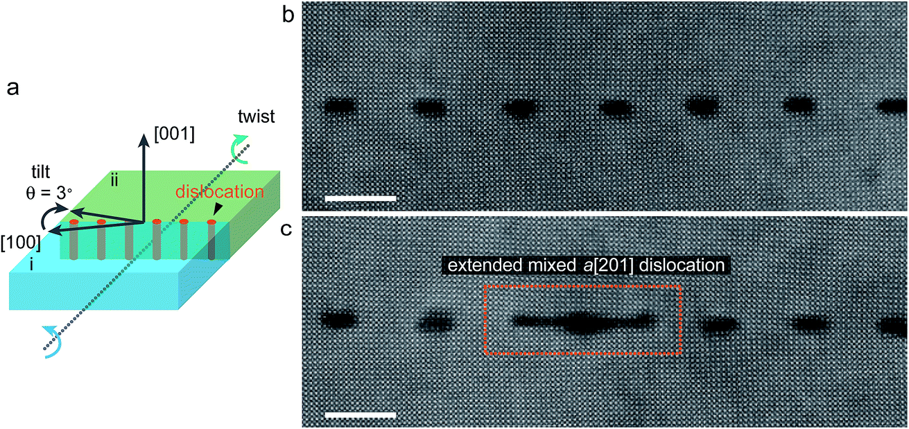 | ||
| Fig. 1 The 3° 〈001〉/{100} tilt grain boundary in SrTiO3 bicrystals. (a) Schematic illustration of the tilt grain boundary with a small twist. (b) HAADF-STEM image of the tilt grain boundary comprising normal dislocations. (c) HAADF-STEM image of the tilt grain boundary with an extended mixed a[201] dislocation related to the presence of a small twist component superimposed on the tilt boundary. The images were recorded at 200 kV acceleration voltages (scale bar: 5 nm). | ||
Fig. 2 shows an atomic resolution HAADF-STEM image of the extended mixed dislocation core. The dislocation comprises three dislocations, a complete dislocation (b = a[100]) located between two partial dislocations (b = a/2[101]) along the tilt grain boundary. Please note that the screw component along the [001] viewing direction is not visible. In the atomic resolution HAADF-STEM image, the intensity is approximately in proportion to Z2, where Z is the atomic number, whereby the brighter and less bright contrast corresponds to the Sr and Ti–O columns, respectively. However, caution should be exercised at the dislocation cores, where intermixing of different types of atoms, partial occupancy of atoms, as well as deviations of atoms from a line along the projection direction may occur and thus considerably influence the intensity of the HAADF-STEM image. Hence, we used the atomic-scale EDX spectrum imaging technique to investigate the chemistry of the atomic columns at the core areas. The atomic resolution EDX maps for Sr and Ti elements are shown also in Fig. 2, which provide direct evidence for Ti enrichment at the dislocation core of the middle b = a[100] complete dislocation. The observed atomic structure of the dislocation cores is rather more complicated than the structural model proposed in the previous report.18
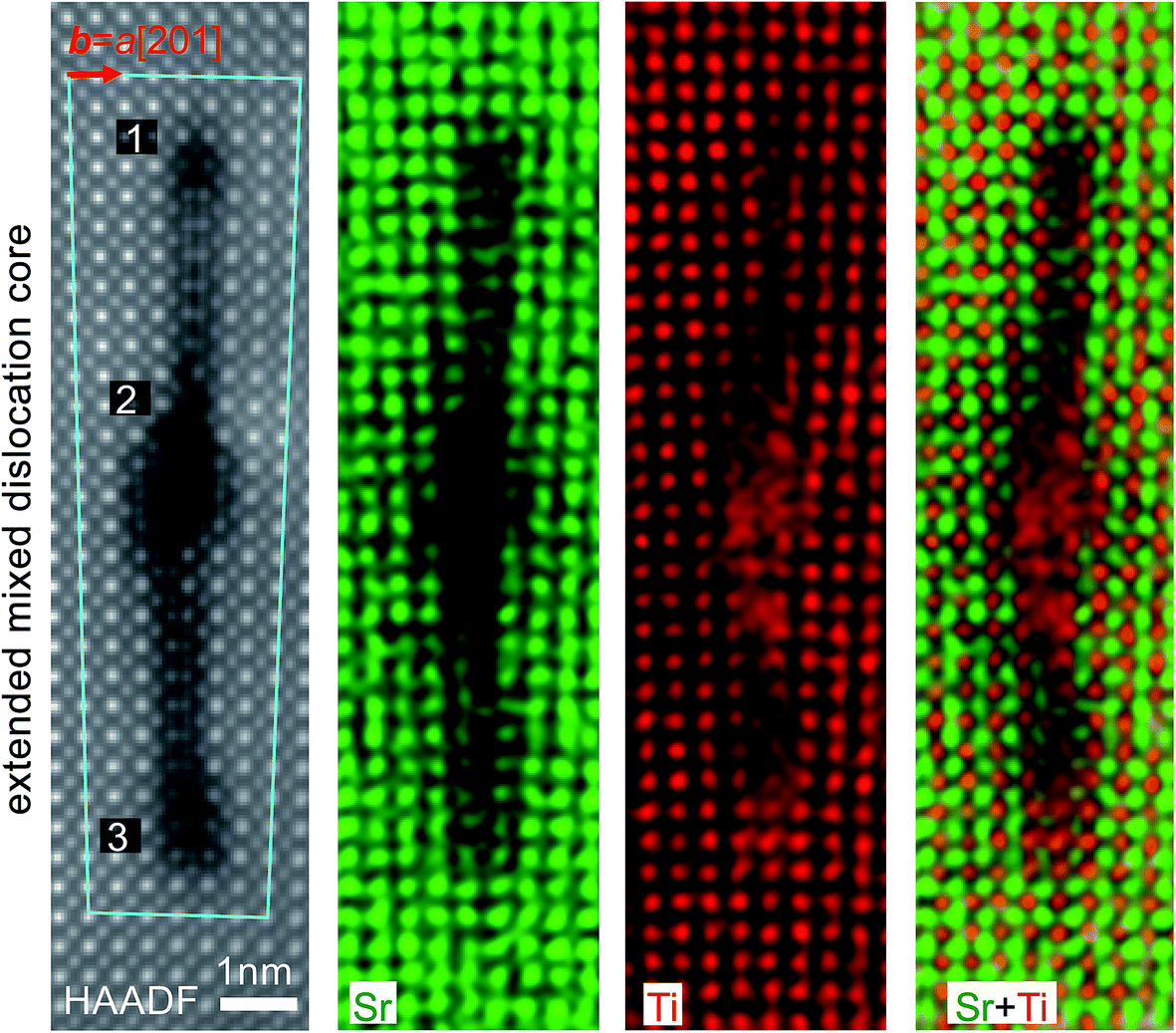 | ||
| Fig. 2 HAADF-STEM image and EDX element maps of the extended dislocation at the 3° 〈001〉/{100} tilt grain boundary in SrTiO3 bicrystals imaged along the [001] zone axis. The extended dislocation comprises a complete dislocation “2” with Burgers vector b = a[100] and two partial mixed dislocations “1” and “3” with b = a/2[101] extended through a stacking fault to the middle b = a[100] complete dislocation “2”. Images were recorded at 200 kV acceleration voltages. | ||
Core-loss electron EELS probes the excitation of electrons from deeply bound initial core states to final unoccupied electronic states above the Fermi level by electric dipole transitions. The initial states are characteristic of the specific type of atom, whereas the final states correspond to the unoccupied partial density of states of the selected atom that is allowed by the electric dipole selection rule with the presence of a core hole. Core-loss EELS spectra therefore provide local chemistry, bonding and electronic structure including both the atomic and electronic arrangements.27 In the present work, we applied core-loss EELS to characterize the Ti–O bonding at the dislocation cores and the stacking faults. Fig. 3 shows the EELS spectra of Ti L2,3 and O K edges. The Ti L2,3 spectrum from the middle b = a[100] complete dislocation core is very similar to that of TiO phase with a NaCl type structure,28 for which the crystal field splitting of the L2 and L3 peaks almost completely vanishes. Correspondingly, the fine structure details for the O K EELS spectrum from the dislocation core significantly diminish in comparison with those from the normal SrTiO3 lattice away from the dislocation core, which is further consistent with those of the TiO phase.28 According to the wide chemical composition range for the FCC-type TiOx (x = 0.66–1.24) phase with structural homogeneity,29 the valence state of the Ti atoms at the dislocation core is therefore referred to as (2 + δ)+, where δ can be from −0.68 to +0.48. As shown in Fig. 3, the Ti(2+δ)+ mainly distributes at the core area of the middle b = a[100] complete dislocation, and is also found along the stacking faults up to the two b = a/2[101] partial mixed dislocation cores.
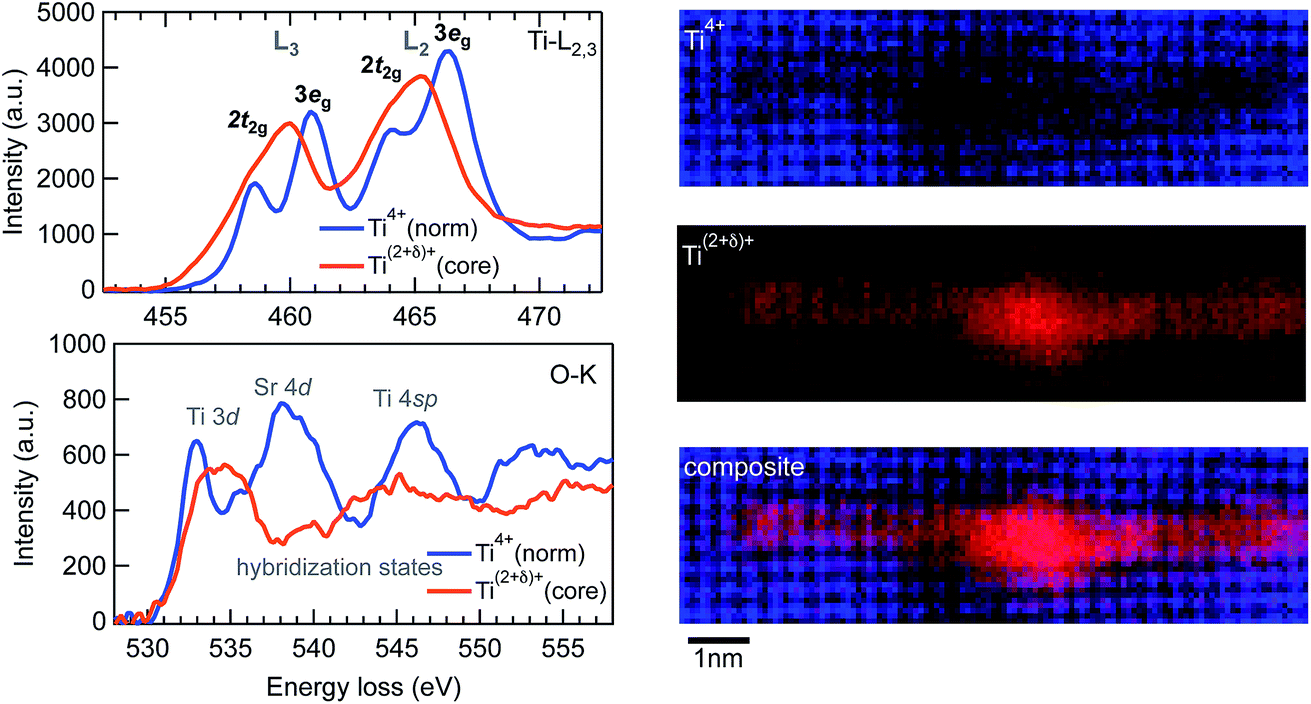 | ||
| Fig. 3 EELS spectra of Ti-L2,3 and O-K edges and the Ti4+ and the Ti(2+δ)+ distribution maps of the extended mixed dislocation cores shown in Fig. 2. The maps were rotated 90° to the left with respect to the HAADF image shown in Fig. 2. | ||
Atomic scale imaging of the b = a[100] edge dislocations
For comparison, HAADF-STEM and EELS/EDX spectrum imaging were conducted from the b = a[100] edge dislocations at the 3° 〈001〉/{100} tilt grain boundary without the presence of a twist. Fig. 4 shows the HAADF-STEM image and EDX maps of Sr and Ti elements at two adjacent b = a[100] edge dislocations. The respective upper and lower core structures delocalize to 4 × 5 and 3 × 4 unit cells in the x and y directions. Similar to the b = a[100] edge dislocations observed at the 6° 〈001〉/{100} tilt grain boundary,15 the dislocation cores also show additional bright dots other than the Sr and Ti–O columns in the HAADF-STEM image. EDX mapping indicates that the additional bright dots correspond to Ti-containing columns, and hence evidences the formation of TiO-like blocks with edge-sharing TiO6 octahedra.15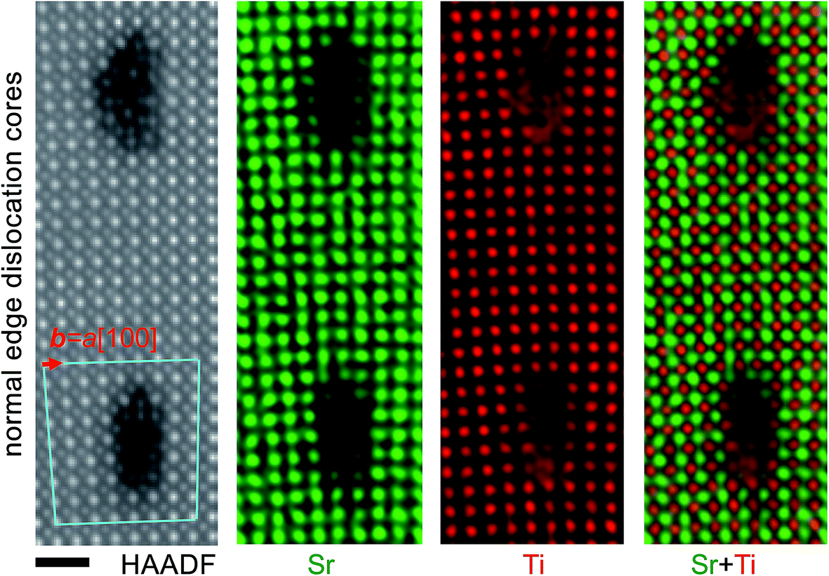 | ||
| Fig. 4 HAADF-STEM image and EDX spectrum maps of normal b = a[100] dislocations at the 3° 〈001〉/{100} tilt grain boundary in SrTiO3 bicrystals recorded at 200 kV acceleration voltage. | ||
Fig. 5 shows the core-loss EELS spectra of Ti L2,3 and O K edges obtained at the lower dislocation core shown in Fig. 4. The Ti L2,3 core-loss spectrum from the dislocation core has less crystal field splitting of the L2 and L3 peaks evident than the normal Ti4+ spectrum from locations away from the dislocation core. But the crystal field splitting of the L2 and L3 peaks from this normal b = a[100] edge dislocation is still visible, being different from that of the middle b = a[100] complete dislocation core in the extended mixed dislocation, for which the splitting almost completely disappears. The peak corresponding to the hybridization of O 2p and Sr 4d states in the O K edge decreases for the spectrum from the dislocation core compared with that from the normal SrTiO3 around the dislocation core. These observations indicate a lower valence state than normal 4+ of the Ti atoms at the Ti-rich dislocation core.
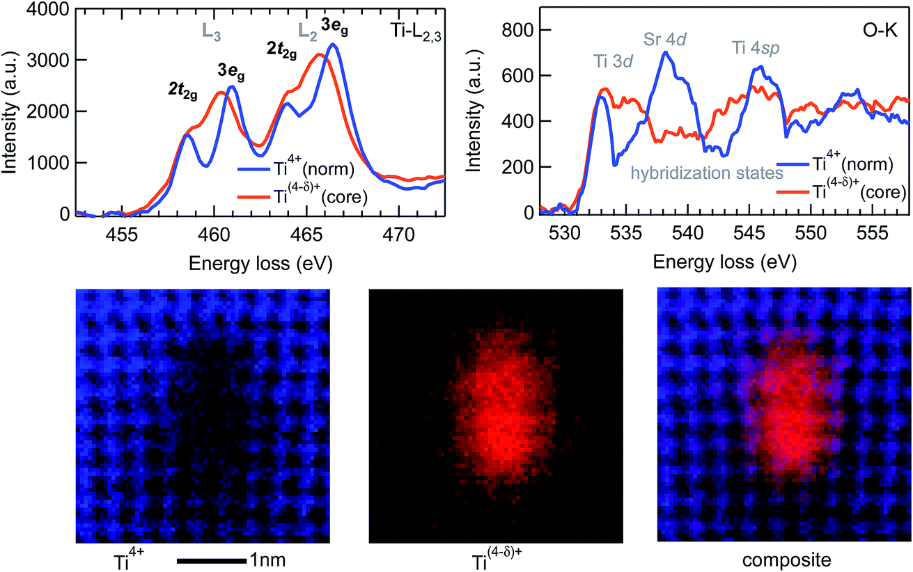 | ||
| Fig. 5 EELS spectra of Ti-L2,3 and O-K edges and the Ti4+ and the Ti(4−δ)+ distribution maps of the b = a[100] dislocation shown in the lower part of Fig. 4. | ||
Atomic structural model and multislice image simulation
Based on the experimental results from the atomic-scale imaging by HAADF-STEM, core-loss EELS, and EDX spectroscopy, atomic structural models for the b = a/2[101] partial dislocation core and for the b = a[100] complete dislocation core with segregation of a TiO phase were constructed. Fig. 6a shows the structural model for the core of the b = a/2[101] partial dislocation, projected along the [001] direction. A close view of the octahedral configuration of TiO6 and the atomic arrangement of the stacking fault projected along the [010] direction is shown in Fig. 6b and c, respectively. In the structure model the Sr and Ti atomic positions in the a–b plane were determined by fitting the column peaks of the experimental HAADF-STEM image with a 2D Gaussian function.30 The constructed atomic structural model for the b = a/2[101] partial dislocation core is more complicated than a simple stacking fault scenario formed by missing a {001} Sr–O layer that has been previously proposed.18 As shown in Fig. 6a, at the dislocation core a Ti–O column is missed (red dot circle). Two additional Ti–O columns (red shaded TiO6) appear in which each octahedral TiO6 shares edges with three adjacent TiO6 to form an edge-sharing TiO6 structure (Fig. 6b). The stacking fault, through which the b = a/2[101] mixed partial dislocation core is extended to the b = a[100] complete dislocation core, appears to be reconstructed rather than two neighboring {100} Ti–O lattice planes. As shown in Fig. 6c, the respective blue and yellow TiO6 octahedra are assigned to the left and right SrTiO3 lattices. As a consequence of the inter-faceting, the stacking fault has a finite region of 0.5 unit cells in the a-axis direction and comprises alternate edge-sharing TiO6 octahedral blocks and Sr atom pairs when viewing along the c-axis. The atomic structure of the reconstructed stacking fault can therefore be described as a combination of local crystallographic shear and faceting on a unit-cell scale.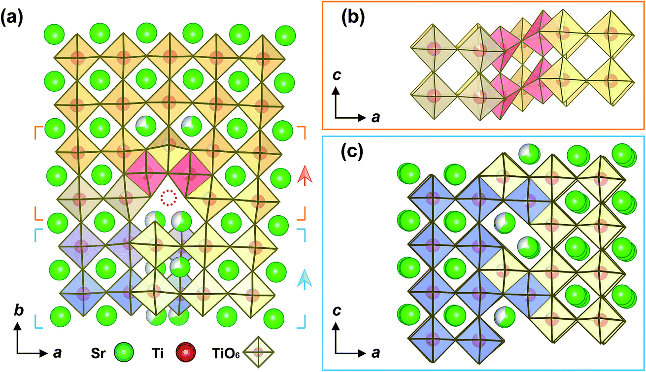 | ||
| Fig. 6 Atomic structure of the b = a/2[101] mixed partial dislocation core. (a) Structural model of the b = a/2[101] mixed partial dislocation core projected against the [001] direction constructed using the atomic positions in the a–b plane measured from the experimental HAADF image. Oxygen atoms are omitted for clarity. The TiO6 octahedra in red at the dislocation core share edges with three adjacent TiO6. The TiO6 octahedra in blue and yellow at the antiphase boundary can be considered to belong to the respective left and right sides of the perovskite lattice. The yellow and blue marks indicate the respective parts shown in (b) and (c), wherein the arrows indicate the viewing direction. (b) Close view of the configuration of TiO6 octahedra at the mixed partial dislocation core. (c) Atomic structure of the stacking fault through which the b = a/2[101] mixed partial dislocation core extends to the b = a[100] complete dislocation core. | ||
Based on the atomic structural model, multislice image simulations were performed. Fig. 7 shows the close comparison between the experimental and the multislice simulated HAADF-STEM images of the b = a/2[101] partial dislocation. A good match between the experimental and simulated images is achieved by taking the partial occupancy of Sr and Ti atoms into account, which is indicated by the maximum of their cross correlation of more than 0.92.
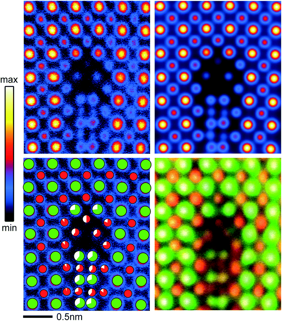 | ||
| Fig. 7 Comparison between the experimental and multislice simulated HAADF-STEM images of the b = a/2[101] mixed partial dislocation core “1” in Fig. 2 projected along the [001] direction. Top: experimental (left) and multislice simulated (right) images, bottom: experimental image (left) marked with green symbols for the Sr columns and red for the Ti–O columns and composite image (right) of HAADF (gray) and EDX maps (green for Sr and red for Ti). The white sector of the symbol indicates the under-occupancy of the respective atomic column. | ||
Fig. 8a shows a magnified HAADF-STEM image with false color of the b = a[100] complete dislocation core. In the image, the dots with a brighter contrast (red-yellow) indicate the heavy Sr columns, whereas dots with a less bright contrast (blue-pink) signify the light Ti–O columns. The segregation of TiO phase at the dislocation core is clearly manifested by a distinct decrease of column intensity and the appearance of extra columns with respect to the HAADF image of the normal SrTiO3 lattice. As shown in Fig. 8b, a TiO phase with width of 1.5 u.c. can be naturally incorporated in the dislocation core, i.e. between two SrTiO3 crystal parts, which have a relative displacement of a/2[001] and are terminated with Ti–O (100) planes, thereby forming local crystallographic shear structures.
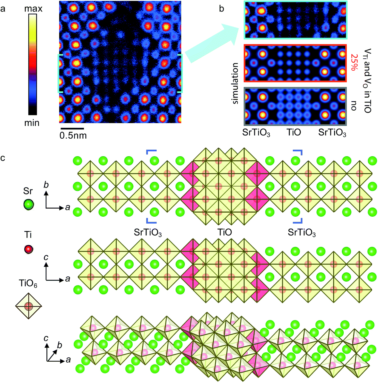 | ||
| Fig. 8 Atomic structure of the b = a[100] complete dislocation core “2” in Fig. 2 of the extended dislocation. (a) Experimental HAADF-STEM image of the complete dislocation core. (b) Comparison between the experimental HAADF-STEM image and multislice simulated images, with and without consideration of 25% of vacancies for both Ti and O atoms in the TiO block from the region of the SrTiO3/TiO/SrTiO3 structural model marked in (c). (c) SrTiO3/TiO/SrTiO3 structural model for the b = a[100] complete dislocation core viewed along different axes. The TiO6 octahedra in red are ascribed to SrTiO3 lattices and share edges with the adjacent TiO6 octahedra from the TiO lattice. Please note that across the dislocation core along the a-axis direction, the SrTiO3 lattice has a a/2[001] displacement in the c-axis direction. | ||
Multislice image simulations were performed from the marked region of a SrTiO3/TiO/SrTiO3 structural model in Fig. 8b both with (Fig. 8a right panel, lower) and without (Fig. 8a right panel, upper) consideration of 25% of vacancies for both Ti and O atoms in the TiO block. The reason for the consideration of both Ti and O vacancies is because the FCC-type TiOx has a wide chemical composition range (x = 0.66–1.24) of structural homogeneity,29 and contains a high equilibrium concentration of vacancies in both the Ti- and O-sublattices,31,32 even for stoichiometric TiO.33 As seen from the right panel of Fig. 8a, the simulated image with consideration of both Ti and O vacancies shows a better match with the experimental image than that without consideration of atomic vacancies. Therefore, in addition to the direct evidence from EELS and EDX results, the multislice image simulation further supports the formation of a TiOx phase at the b = a[100] complete dislocation core (Fig. 8b).
Discussion
Similar to the a[100] edge dislocations found at low-angle tilt grain boundary, local TiO6 octahedra sharing edges is a unique feature for the atomic structure of the b = a[201]/(100) extended mixed dislocation, including the core structures of the b = a/2[101] partial dislocation, the b = a[100] complete dislocation, and the stacking faults. In perovskite-related materials, structures comprising edge- or face-sharing MO6 octahedra instead of corner-sharing in their parent structures have been known for a long time as crystallographic shear (CS) structures.34 This provides the rationale for us to name local atomic structures consisting of metal–oxygen (M–O) octahedra sharing edges in perovskite materials as local crystallographic shear (LCS) structures. Defects in perovskite oxides comprising LCS structures therefore can be classified as LCS-type defects.CS structures commonly occur in anion-deficient oxides, e.g., WnO3n−2, (Mo,W)nO3n−2, TinO2n−1, etc., derived from the ReO3 or rutile (TiO2) structures based on metal-centered MO6 coordination octahedra,34 but rarely occur in the perovskite structure on the macro-scale.34,35 Interestingly, LCS structures have been revealed by TEM in WO3–Nb2O5 (ref. 36) and TiO2–Nb2O5 (ref. 37 and 38) oxide systems dating back to the late 1960s. Later on electron-paramagnetic-resonance measurements have also revealed the existence of corner-shared TiO6–TiO6 octahedra in Ti-rich planar defects of oxygen-deficient rutile TiO2.47 In particular, with the application of aberration-corrected TEM imaging techniques, an increasing number of LCS structures were observed at defects in different perovskite oxides including SrTiO3,24,39,48 BaTiO3,40 Ba-doped Na0.5Bi0.5TiO3,41 and (Nd,Ti)-codoped Bi0.9Nd0.15FeO3.42,43 These observations indicate that LCS-type defects appear to be common in B-rich ABO3 perovskite oxides. Nevertheless, these observed local structures consisting of edge-sharing MO6 octahedra have not been correlated with the well-known CS structures, and hence LCS-type defects have received much less attention than the well-known Ruddlesden–Popper-type defects in perovskite oxides.44 More studies are therefore needed in order to understand how LCS-type defects alter local material properties.
Another prominent feature for the middle b = a[100] complete dislocation in the b = a[201]/(100) extended mixed dislocation is nanosized TiO phase segregated at the dislocation core along the dislocation line. The formation of the TiOx phase can be understood as a result of tensional and shear strain from the tilt and twist between the two crystal parts. Because of the larger lattice constant of the FCC TiO phase (a = 0.42 nm) than SrTiO3 (0.39 nm), forming the TiOx phase can accommodate tensional strain, and thus lowers the system energy.15 On the other hand, a TiOx phase can be naturally incorporated between two SrTiO3 crystal parts with a relative displacement of a/2[001] through forming local crystallographic shear structures (Fig. 8c), thereby accommodating the shear strain from the small twist.
The TiOx derived from the FCC-type structure is of particular interest because it tolerates a wide chemical composition range (x = 0.66–1.24) of structural homogeneity,29 and contains a high equilibrium concentration of vacancies in both the Ti- and O-sublattices,31,32 even for stoichiometric TiO.33 Moreover, these vacancies can be distributed either randomly or in an ordered way at the sites of the sublattices.45 Furthermore, in contrast to TiO2 phases being insulators or wide-band gap semiconductors, TiOx exhibits either semiconducting or metallic conductivity with electrical resistivity of only several μΩ cm.46 From this perspective, dislocations comprising TiOx phase at their cores are of particular interest for study of resistive switching phenomena via changing the oxygen content of the TiOx phase through electrically stimulated redox reactions.
Locally conducting atomic force microscopy measurements have revealed that conducting filaments can be preferentially created along the SrTiO3 bicrystal boundary due to the easy reduction of the dislocation cores.10 On the other hand, the electric conductivity for the cubic titanium monoxides TiOx varies with the oxygen content x.46 A conceivable configuration of a resistive switching device making use of the extended mixed dislocation core is illustrated in Fig. 9. The oxygen content of the TiOx phase could be adjusted by electric-field-induced redox reactions, thereby, setting different resistance states along the dislocation core. Please note that Fig. 9 illustrates a situation where the rate of oxygen release (incorporation) at the electrode is faster (slower) than that of the oxygen migration inside the material. In an opposite case, the variation of oxygen content should be reversed.26
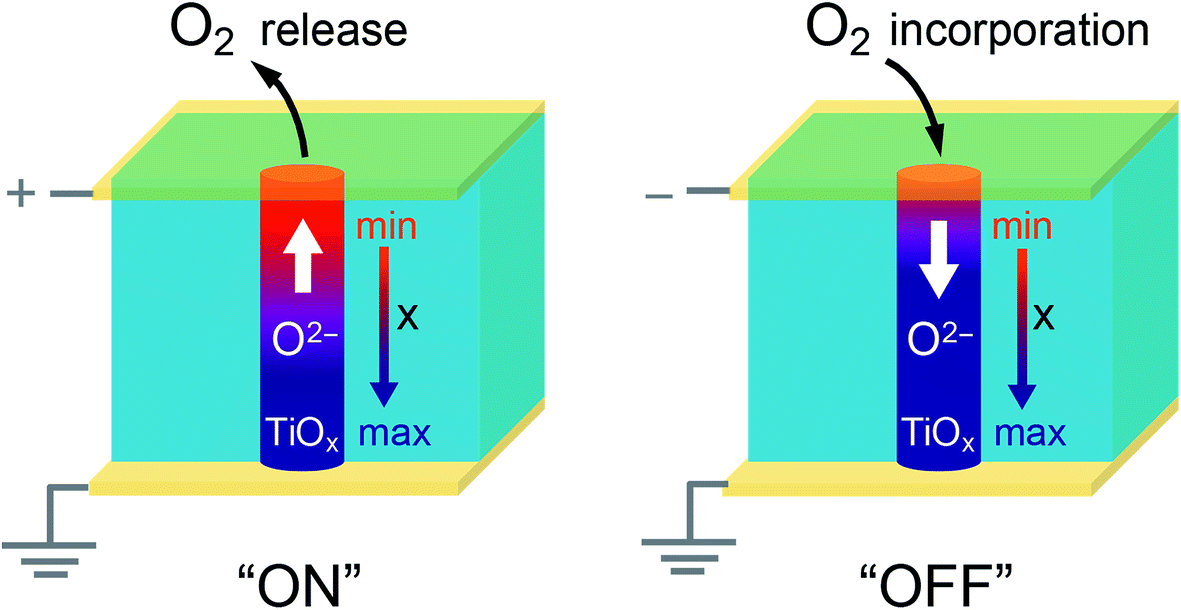 | ||
| Fig. 9 Schematic of a conceivable resistive switching configuration making use of the extended mixed dislocation core comprising a TiOx phase, under a situation where the rate of oxygen release (incorporation) at the electrode is faster (slower) than that of the migration of oxygen inside the lattice of the material. | ||
Conclusion
In conclusion, the atomic details of the extended mixed [201]/(100) dislocations at 3° low-angle 〈001〉/{100} tilt grain boundaries of a SrTiO3 bicrystal have been comprehensively studied using complementary atomic-scale imaging techniques of STEM, EELS, and EDX spectroscopy, as well as multislice image simulations. The atomic details of the b = a[201]/(100) extended mixed dislocation evidenced by our work is much more complicated than a simple stacking fault scenario. A unique feature for the atomic structure of the b = a[201]/(100) extended mixed dislocation is the local crystallographic shear (LCS) structures, where TiO6 octahedra share edges instead of corners at the cores of the b = a/2[101] partial dislocation and the b = a[100] complete dislocation. A survey of literature indicates that LCS-type defects appear to be common in B-rich ABO3 perovskite oxides, which should deserve particular attention in order to understand their impact on local material properties.Moreover, we have observed an evident segregation of one-dimensional-like FCC TiOx phase at the middle b = a[100] complete dislocation core. The formation of the TiOx phase can be understood as a result of tensional and shear strain from the tilt and twist between the two crystal parts. The dislocation core with a segregation of one-dimensional-like FCC TiOx phase appears to be a particularly interesting system for resistive switching, via a conceivable mechanism of completion and disruption of the TiOx phase through electrically stimulated redox reactions.
Conflicts of interest
The authors declare no conflicts of interest.Acknowledgements
We thank Doris Meertens for preparation of the TEM lamellae by FIB. We acknowledge support from the Deutsche Forschungsgemeinschaft (DFG) under Grant SFB 917 Nanoswitches and under the core facilities Grant MA 1280/40-1. We appreciate Kristof Szot for insightful discussion on making use of dislocation cores for resistive switching.References
- M. A. Peña and J. L. G. Fierro, Chem. Rev., 2001, 101, 1981–2018 CrossRef.
- J. G. Bednorz and K. A. Müller, Zeitschrift für Physik. B, 1986, 64, 189–193 CrossRef CAS.
- C. W. Nelson, Ferroelectricity and the Chemical Bond in Perovskite-Type Oxides, Massachusetts Institute of Technology, Cambridge, Massachusetts, 1963 Search PubMed.
- Mixed Ionic Electronic Conducting Perovskites for Advanced Energy Systems, ed. N. Orlovskaya and N. Browning, Springer, Netherlands, Dordrecht, 2004 Search PubMed.
- H. Ohta, S. Kim, Y. Mune, T. Mizoguchi, K. Nomura, S. Ohta, T. Nomura, Y. Nakanishi, Y. Ikuhara, M. Hirano, H. Hosono and K. Koumoto, Nat. Mater., 2007, 6, 129–134 CrossRef CAS.
- C. Jia, S. Mi, K. Urban, I. Vrejoiu, M. Alexe and D. Hesse, Phys. Rev. Lett., 2009, 102, 117601 CrossRef CAS.
- K. Szot, W. Speier, G. Bihlmayer and R. Waser, Nat. Mater., 2006, 5, 312–320 CrossRef CAS PubMed.
- R. J. Kamaladasa, M. Noman, W. Chen, P. A. Salvador, J. A. Bain, M. Skowronski and Y. N. Picard, J. Appl. Phys., 2013, 113, 234510 CrossRef.
- C. Lenser, Z. Connell, A. Kovács, R. Dunin-Borkowski, A. Köhl, R. Waser and R. Dittmann, Appl. Phys. Lett., 2013, 102, 183504 CrossRef.
- K. Szot, C. Rodenbücher, G. Bihlmayer, W. Speier, R. Ishikawa, N. Shibata and Y. Ikuhara, Crystals, 2018, 8, 241 CrossRef.
- V. Metlenko, A. H. H. Ramadan, F. Gunkel, H. Du, H. Schraknepper, S. Hoffmann-Eifert, R. Dittmann, R. Waser and R. A. De Souza, Nanoscale, 2014, 6, 12864–12876 RSC.
- R. A. De Souza, J. Fleig, J. Maier, Z. Zhang, W. Sigle and M. Rühle, J. Appl. Phys., 2005, 97, 053502 CrossRef.
- R. A. De Souza, J. Fleig, J. Maier, O. Kienzle, Z. Zhang, W. Sigle and M. Rühle, J. Am. Ceram. Soc., 2003, 86, 922–928 CrossRef CAS.
- R. Waser, R. Dittmann, G. Staikov and K. Szot, Adv. Mater., 2009, 21, 2632–2663 CrossRef CAS.
- H. Du, C.-L. Jia, L. Houben, V. Metlenko, R. A. De Souza, R. Waser and J. Mayer, Acta Mater., 2015, 89, 344–351 CrossRef CAS.
- Z. Zhang, W. Sigle, R. A. De Souza, W. Kurtz, J. Maier and M. Rühle, Acta Mater., 2005, 53, 5007–5015 CrossRef CAS.
- P. Gao, R. Ishikawa, B. Feng, A. Kumamoto, N. Shibata and Y. Ikuhara, Ultramicroscopy, 2018, 184, 217–224 CrossRef CAS.
- Y. Furushima, Y. Arakawa, A. Nakamura, E. Tochigi and K. Matsunaga, Acta Mater., 2017, 135, 103–111 CrossRef CAS.
- D. Meertens, M. Kruth and K. Tillmann, Journal of Large-Scale Research Facilities JLSRF, 2016, 2, A60 CrossRef.
- A. Kovács, R. Schierholz and K. Tillmann, Journal of Large-Scale Research Facilities JLSRF, 2016, 2, A43 CrossRef.
- K. Tillmann, J. Barthel and L. Houben, Journal of Large-Scale Research Facilities JLSRF, 2015, 1, A34 CrossRef.
- J. Barthel, Dr. Probe-STEM simulation software, http://www.er-c.org/barthel/drprobe/, 2016 Search PubMed.
- K. Momma and F. Izumi, J. Appl. Crystallogr., 2011, 44, 1272–1276 CrossRef CAS.
- H. Du, C.-L. Jia, J. Mayer, J. Barthel, C. Lenser and R. Dittmann, Adv. Funct. Mater., 2015, 25, 6369–6373 CrossRef CAS.
- H. Du, Ultramicroscopy, 2015, 151, 62–67 CrossRef CAS.
- H. Du, C.-L. Jia, A. Koehl, J. Barthel, R. Dittmann, R. Waser and J. Mayer, Chem. Mater., 2017, 29, 3164–3173 CrossRef CAS.
- J. Silcox, Curr. Opin. Solid State Mater. Sci., 1998, 3, 336–342 CrossRef CAS.
- E. Stoyanov, F. Langenhorst and G. Steinle-Neumann, Am. Mineral., 2007, 92, 577–586 CrossRef CAS.
- H. Okamoto, J. Phase Equilib. Diffus., 2011, 32, 473–474 CrossRef CAS.
- H. Du, C.-L. Jia and J. Mayer, Chem. Mater., 2016, 28, 650–656 CrossRef CAS.
- S. P. Denker, J. Phys. Chem. Solids, 1964, 25, 1397–1405 CrossRef CAS.
- A. A. Valeeva, A. A. Rempel, W. Sprengel and H.-E. Schaefer, Phys. Rev. B: Condens. Matter Mater. Phys., 2007, 75, 094107 CrossRef.
- D. Watanabe, J. R. Castles, A. Jostsons and A. S. Malin, Nature, 1966, 210, 934–936 CrossRef CAS.
- S. Andersson and A. D. Wadsley, Nature, 1966, 211, 581–583 CrossRef CAS.
- A. M. Abakumov, J. Hadermann, S. Bals, I. V. Nikolaev, E. V. Antipov and G. Van Tendeloo, Angew. Chem., 2006, 118, 6849–6852 CrossRef.
- J. G. Allpress, J. V. Sanders and A. D. Wadsley, Acta Crystallogr., Sect. B: Struct. Crystallogr. Cryst. Chem., 1969, 25, 1156–1164 CrossRef CAS.
- J. G. Allpress, J. Solid State Chem., 1969, 1, 66–81 CrossRef CAS.
- S. Iijima, J. Appl. Phys., 1971, 42, 5891 CrossRef CAS.
- C. Jia, A. Thust and K. Urban, Phys. Rev. Lett., 2005, 95, 225506 CrossRef CAS PubMed.
- C. L. Jia and A. Thust, Phys. Rev. Lett., 1999, 82, 4 Search PubMed.
- X.-W. Jin, L. Lu, S.-B. Mi, S. Cheng, M. Liu and C.-L. Jia, J. Alloys Compd., 2016, 676, 173–180 CrossRef CAS.
- I. MacLaren, L. Wang, A. J. Craven, Q. M. Ramasse, B. Schaffer, K. Kalantari and I. M. Reaney, APL Mater., 2014, 2, 066106 CrossRef.
- J. M. Salih, L. Q. Wang, Q. M. Ramasse, L. Jones, J. Barthel, I. M. Reaney, A. J. Craven and I. MacLaren, Mater. Sci. Technol., 2016, 1–6 CrossRef.
- C. Xu, H. Du, A. J. H. van der Torren, J. Aarts, C.-L. Jia and R. Dittmann, Sci. Rep., 2016, 6, 38296 CrossRef CAS PubMed.
- M. G. Kostenko, A. V. Lukoyanov, V. P. Zhukov and A. A. Rempel, J. Solid State Chem., 2013, 204, 146–152 CrossRef CAS.
- A. A. Valeeva, A. A. Rempel and A. I. Gusev, JETP Lett., 2001, 73, 621–625 CrossRef CAS.
- M. Aono and R. R. Hasiguti, Phys. Rev. B: Condens. Matter Mater. Phys., 1993, 48, 12406–12414 CrossRef CAS.
- D. Wrana, C. Rodenbücher, B. R. Jany, O. Kryshtal, G. Cempura, A. Kruk, P. Indyka, K. Szot and F. Krok, Nanoscale, 2018 10.1039/c8nr04545c.
| This journal is © The Royal Society of Chemistry 2019 |