
 Open Access Article
 This Open Access Article is licensed under a
 Creative Commons Attribution 3.0 Unported Licence
An interface stabilized perovskite solar cell with high stabilized efficiency and low voltage loss†
Jason J.
Yoo
 a,
Sarah
Wieghold
b,
Melany C.
Sponseller
c,
Matthew R.
Chua
c,
Sophie N.
Bertram
a,
Noor Titan Putri
Hartono
b,
Jason S.
Tresback
d,
Eric C.
Hansen
a,
Juan-Pablo
Correa-Baena
b,
Vladimir
Bulović
c,
Tonio
Buonassisi
b,
Seong Sik
Shin
*be and
Moungi G.
Bawendi
*a
a,
Sarah
Wieghold
b,
Melany C.
Sponseller
c,
Matthew R.
Chua
c,
Sophie N.
Bertram
a,
Noor Titan Putri
Hartono
b,
Jason S.
Tresback
d,
Eric C.
Hansen
a,
Juan-Pablo
Correa-Baena
b,
Vladimir
Bulović
c,
Tonio
Buonassisi
b,
Seong Sik
Shin
*be and
Moungi G.
Bawendi
*a
aDepartment of Chemistry, Massachusetts Institute of Technology, 77 Massachusetts Avenue, Cambridge, Massachusetts 02139, USA. E-mail: mgb@mit.edu
bDepartment of Mechanical Engineering, Massachusetts Institute of Technology, 77 Massachusetts Avenue, Cambridge, Massachusetts 02139, USA
cDepartment of Electrical Engineering and Computer Science, Massachusetts Institute of Technology, 77 Massachusetts Avenue, Cambridge, Massachusetts 02139, USA
dCenter for Nanoscale Systems, Harvard University, Cambridge, Massachusetts 02138, USA
eDivision of Advanced Materials, Korea Research Institute of Chemical Technology, 141 Gajeong-Ro, Yuseong-Gu, Daejeon 34114, Korea. E-mail: sss85@krict.re.kr
First published on 20th June 2019
Abstract
Stabilization of the crystal phase of inorganic/organic lead halide perovskites is critical for their high performance optoelectronic devices. However, due to the highly ionic nature of perovskite crystals, even phase stabilized polycrystalline perovskites can undergo undesirable phase transitions when exposed to a destabilizing environment. While various surface passivating agents have been developed to improve the device performance of perovskite solar cells, conventional deposition methods using a protic polar solvent, mainly isopropyl alcohol (IPA), results in a destabilization of the underlying perovskite layer and an undesirable degradation of device properties. We demonstrate the hidden role of IPA in surface treatments and develop a strategy in which the passivating agent is deposited without destabilizing the high quality perovskite underlayer. This strategy maximizes and stabilizes device performance by suppressing the formation of the perovskite δ-phase and amorphous phase during surface treatment, which is observed using conventional methods. Our strategy also effectively passivates surface and grain boundary defects, minimizing non-radiative recombination sites, and preventing carrier quenching at the perovskite interface. This results in an open-circuit-voltage loss of only ∼340 mV, a champion device with a power conversion efficiency of 23.4% from a reverse current–voltage scan, a device with a record certified stabilized PCE of 22.6%, and enhanced operational stability. In addition, our perovskite solar cell exhibits an electroluminescence external quantum efficiency up to 8.9%.
Broader contextA novel method for depositing low dimensional (LD) perovskite materials onto a bulk 3D perovskite film is investigated. This method can be applied to other surface treatments to improve and stabilize device performance. Up to now, all studies have focused on the structure and the identity of the LD perovskite materials. We report that it is actually the synthetic method that is the most critical factor for fabricating high performance 3D/LD perovskite solar cells; something that has not been investigated and has been overlooked. Our novel strategy results in perovskite devices with high stabilized efficiency of 22.6% and maintains high efficiency (>20%) under maximum power point tracking for ∼500 h under full AM 1.5G illumination, including the ultraviolet, without incorporation of Cs and Rb additives. In addition, we have obtained an open circuit voltage loss of 340 mV for our certified cell, which is the lowest reported so far, along with an unprecedently high electroluminescence efficiency of ∼8.9%. |
Introduction
Perovskite solar cells (PSCs) have been intensively studied in the last few years due to their excellent photovoltaic performance and low fabrication costs.1–3 Recent progress on stabilization of the crystal phase and defect management of inorganic/organic lead halide perovskites has resulted in devices with attractive power conversion efficiencies (PCEs).4–10 Further improvements should be gained through interlayer/surface engineering to passivate interface defects, using metal oxides, polymers, small molecules, or organic halides.11–15 However, conventional surface treatment strategies geared at passivating interface defects have not demonstrated a performance exceeding that of PSCs fabricated simply from 3-dimensional (3D) perovskites. We show that this efficiency gap is due to the hidden role of the solvent that is used in conventional surface treatment method.10,16,17 The use of an inappropriate solvent during surface treatment can negatively affect the underlying perovskite layer, preventing passivating agents from fulfilling their potential. The key challenge in the fabrication of interface passivated PSCs with high PCE and operational stability is to ensure that the underlying 3D perovskite layer remains pristine during surface treatment without negatively affecting its structure and properties.In this study, we report a selective precursor dissolution (SPD) strategy using a unique precursor/solvent combination (linear alkyl ammonium bromides/chloroform) for the effective synthesis of a layered perovskite (LP) onto an underlying 3D perovskite thin film. Although the in situ preparation of a LP passivation layer on a 3D perovskite layer (thereby forming a 3D/LP heterostructure) has gained attention for its potential to effectively passivate interfaces and grain boundary defects, increase moisture resistance, and outperform state of the art single layer 3D devices,18 3D/LP heterostructure devices have not yet delivered on their potential. Compared to previous (conventional) methods, our approach leads to the most effective synthesis of various passivating layers onto 3D perovskite layers without disrupting the underlying 3D perovskite layer; a key for maximizing device performance and stability. The SPD strategy prolongs carrier lifetime through defect passivation and improves the open circuit voltage (VOC). Through this strategy, we obtain a champion device with a PCE of 23.4% from a reverse current–voltage (J–V) sweep with a certified stabilized PCE (measured under stabilized conditions for ∼31 min) of 22.6% – the highest stabilized and certified PCE reported for PSCs thus far – with a VOC loss of only ∼340 mV, which is the lowest VOC loss reported thus far, and with enhanced operational stability. In addition, our PSC shows an electroluminescence (EL) external quantum efficiency (EQE) of up to 8.9%, which is the highest value reported from a PSC.
Results and discussion
Isopropyl alcohol (IPA) is the most popular solvent used in conventional methods for post-processing of perovskite thin films for surface passivation. To understand the effect of this solvent on the underlying perovskite thin film during surface treatment, we compared the solubility of perovskite precursors in IPA relative to a solvent commonly used as a non-solvent; chloroform (CF). IPA effectively dissolves formamidinium iodide (FAI) due to its highly polar nature and its ability to form hydrogen bonds (Fig. 1a). In contrast, CF, a solvent frequently used as the anti-solvent, shows very limited solubility towards FAI (<1 mg mL−1). The effect of solvent on the perovskite is further explored in grazing incident X-ray diffraction (GIXRD), where the 3D perovskite thin film, with the composition (FAPbI3)0.92(MAPbBr3)0.08 (3D perovskite) where MA is methylammonium, is treated with either neat IPA or neat CF (control is without any solvent treatment) (Fig. 1b). Compared to the control, the neat IPA treated perovskite film shows a PbI2 rich surface, likely due to the dissolution and/or decomposition of the ammonium halide salt (Fig. S1, ESI†). In contrast, no visible change is observed for neat CF treated sample. The solubility of n-hexylammonium bromide (C6Br), a passivating agent used for in situ synthesis of LP passivating layer, shows the opposite trend where C6Br shows higher solubility in CF than in IPA (Fig. 1a). Interestingly, other commonly used anti-solvents (chlorobenzene, 1,2-dichlorobenzene, and toluene) did not dissolve the passivating agent and cannot be used during surface passivation (Fig. S1, ESI†). In addition, we tried to dissolve phenylammonium and benzylammonium halides which are mainly used for passivating agents, but these types of ammonium halides were not soluble in CF. Only a unique combination of the linear alkyl ammonium bromide based LP precursors and a specific non-solvent (CF) resulted in a passivating solution that can deliver high quality LP layers onto 3D perovskites without negatively affecting the underlying 3D perovskite layer.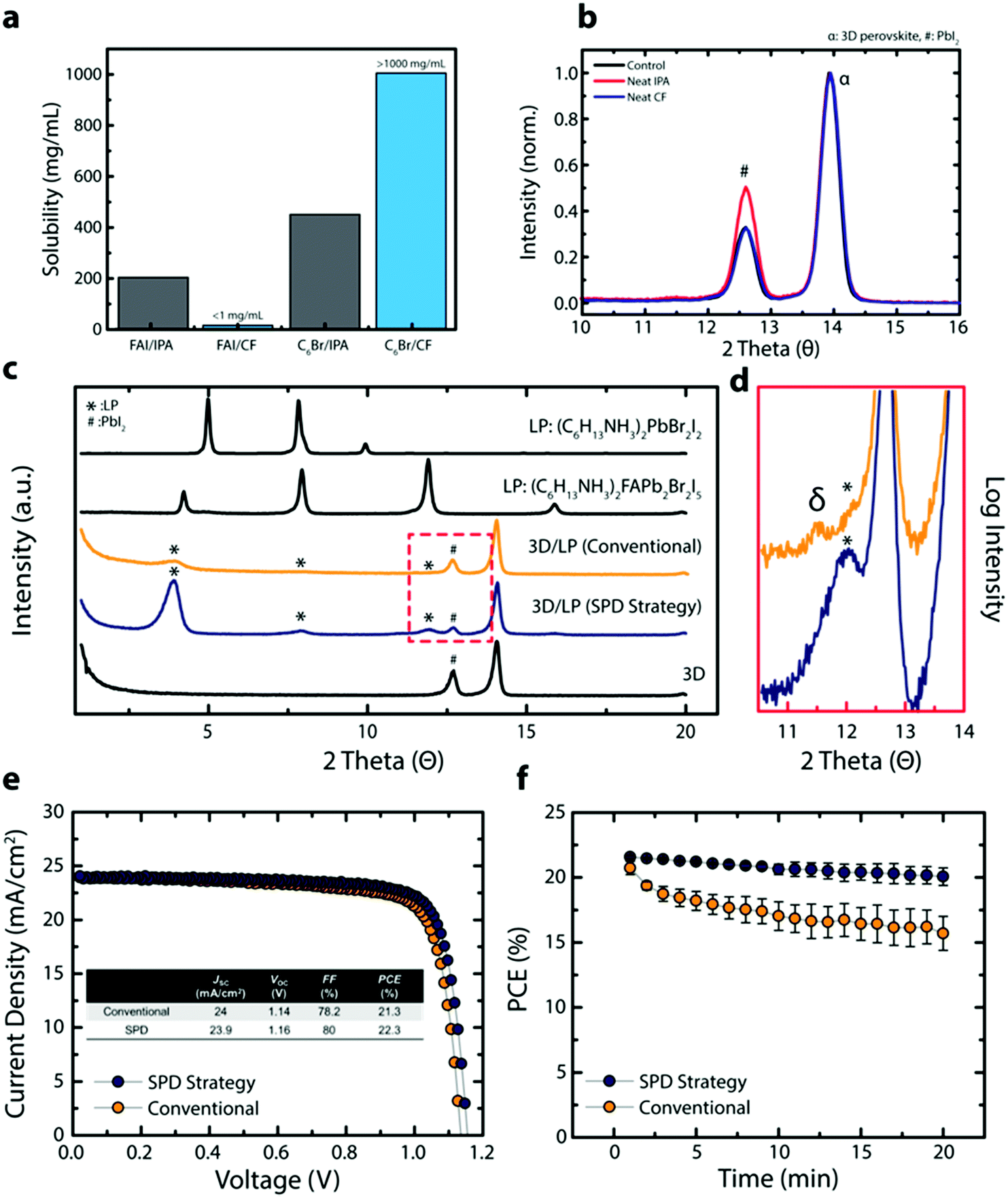 | ||
| Fig. 1 (a) Solubility of FAI and C6Br in CF and IPA illustrating the appropriateness of using CF for the LP treatment. (b) Grazing incident XRD (GIXRD) of 3D perovskite treated without any solvent (control), with neat IPA, or with neat CF. α corresponds to the 3D perovskite diffraction peak and # corresponds to the PbI2 diffraction peak. (c) GIXRD of 3D and 3D/LPs fabricated using IPA (conventional) or CF (SPD strategy), and XRD of pristine LP with different compositions. * corresponds to the LP diffraction peak. (d) XRD of the 3D/LP (conventional) and 3D/LP (SPD strategy) perovskites showing the formation of the δ-phase (∼11.5°) in 3D/LP (conventional) perovskites. (e) J–V curve of 3D/LP (conventional) and 3D/LP (SPD strategy) PSCs. (f) Light stability test of 3D/LP (conventional) and 3D/LP (SPD strategy) PSCs showing higher device performance and stability for 3D/LP (SPD strategy) PSCs. | ||
To further analyze the effect of solvent on 3D perovskite thin films, we compared carrier lifetimes for 3D perovskite films exposed to neat IPA or CF under various conditions (Fig. S1c–e, ESI†). 3D perovskite thin films show slightly reduced carrier lifetimes when exposed to neat IPA for a short time period (<2 s for typical spin-coating method) in an inert environment compared to neat CF. In fact, a bigger difference in the carrier lifetime is observed when the experiment is carried out in an ambient condition (relative humidity ∼30%). In addition, to closely simulate scaled-up fabrication of PSCs where spin coating deposition methods are not feasible, the 3D perovskite films were dipped in an IPA or CF containing C6Br in an ambient condition (relative humidity ∼30%). The 3D perovskite substrate dipped in a n-hexylammonium bromide (C6Br) containing IPA (LP/IPA) solution shows significantly reduced carrier lifetimes, likely due to the hygroscopic nature of the solvent as well as the detrimental effect protic polar solvents have on the perovskite film (Fig. S1b, ESI†). Together with the use of polar solvents, hygroscopic solvents are a critical issue for the scaled-up production of PSCs under ambient conditions. The difference between hygroscopic IPA and non-hygroscopic CF on 3D perovskite films is demonstrated in Fig. S2 (ESI†). The 3D perovskite thin film exposed to neat IPA shows an increase in its absorption baseline above ∼800 nm and decreasing relative absorbance below ∼550 nm as a function of time (0–90 min) (Fig. S2a, ESI†). These changes in optical profile are likely due to changes in the perovskite crystal structure, increasing light scattering, and bleaching of the 3D perovskite film. In contrast, the 3D perovskite thin film submerged in CF shows no change in optical profile even after 90 minutes. The long-term effect of IPA and CF is demonstrated in Fig. S2b (ESI†) where a perovskite powder and thin film are exposed to IPA and CF overnight in air. Both the perovskite powder and the thin film exposed to IPA show severe perovskite bleaching and decomposition whereas the samples retain their color when submerged in CF. CF is immiscible with water, which suggests CF is an ideal solvent system for post-processing perovskite thin films under ambient conditions.
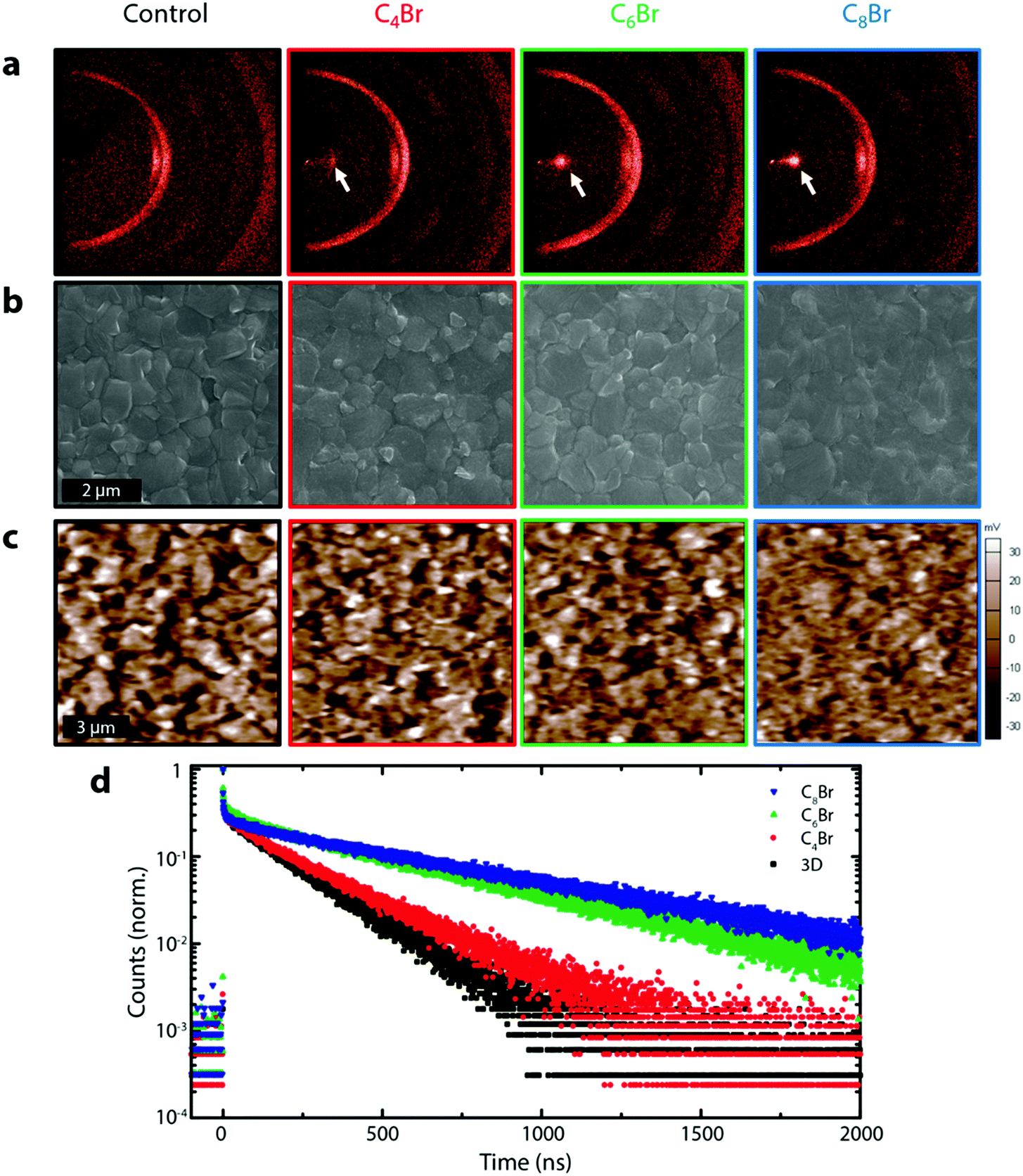 | ||
| Fig. 2 (a) XRD2 image of 3D control and three different 3D/LP (C4Br, C6Br, C8Br) perovskites fabricated using the SPD strategy. White arrows indicate the (001) peak of the LP. (b) Planar SEM of 3D control and 3D/LP samples. (c) KPFM images of 3D control and 3D/LP samples. SEM images show that the grain boundary is less distinct for the 3D/LP and the same behavior is observed in potential mapping from KPFM. (d) TRPL trace of 3D and 3D/LP films deposited on a quartz substrate. The sample was excited through the quartz substrate. An increase in the carrier lifetime is observed with LP treatment. | ||
To confirm the negative effect of IPA and the inertness of CF on device performance, 3D PSCs were fabricated by treating the 3D perovskite active layer with either neat IPA or CF. The neat IPA treated PSCs show lower PCEs on average and a wider PCE distribution compared to devices treated with CF, and faster degradation is observed for neat IPA treated PSC under MPP (Fig. S3, ESI†). Moreover, devices based on 3D perovskite films exposed to CF overnight retain their high efficiencies (Fig. S3c, ESI†) whereas this could not have been possible with PSCs exposed to IPA.
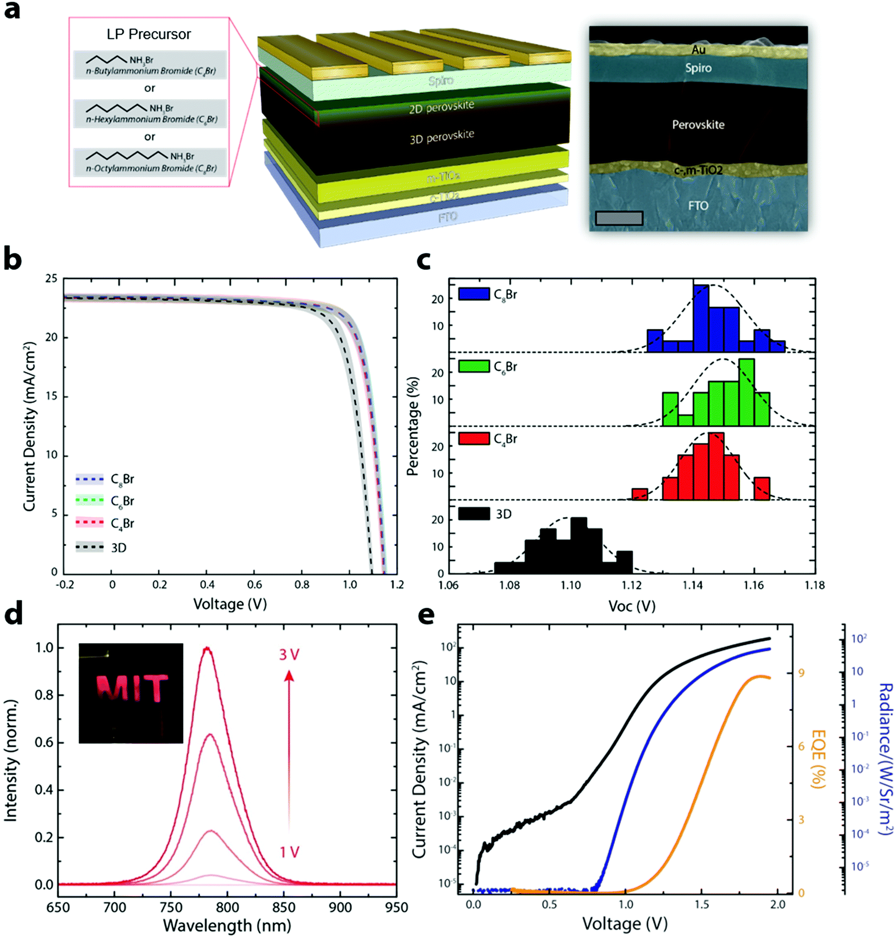 | ||
| Fig. 3 (a) Schematic illustration of a 3D/LP PSC with false colored cross-sectional SEM (scale bar: 500 nm). (b) J–V curves of 3D and 3D/LP (C4Br, C6Br, C8Br) PSCs fabricated using the SPD strategy, with average and standard deviation shown as a dashed line and shaded area, respectively. (c) Histogram of VOC for 3D and 3D/LP (C4Br, C6Br, C8Br) PSCs. (d) Electroluminescence spectra from the SPD strategy based 3D/LP PSC operated as a LED. The inset shows the bright electroluminescence from the device. (e) Plot of current density, EQE, and radiance as a function of voltage. The device shows a max EQE of 8.9%. | ||
Based on the results above, we expect an improved 3D perovskite interface when using CF during the in situ synthesis of a LP passivating layer. Fig. 1c shows XRD results for the 3D perovskite, the 3D perovskite treated with the LP with CF or IPA as solvents and C6Br as the LP precursor (3D/LP (SPD strategy) or 3D/LP (conventional)), and pristine LPs. Compared to the 3D perovskite, 3D/LPs with C6Br treatment have additional peaks at 3.9°, 7.9°, and 11.9° (marked with *) and show a lower peak intensity for the PbI2 peak (marked with #), indicating the incorporation of near-surface PbI2 into the LP during the in situ synthesis of the LP. When comparing XRD peaks from pristine LP films, the LP peaks from 3D/LP structures matches well with the Ruddlesden–Popper hybrid perovskite (C6H13NH3)2(FA)Pb2Br2I5 compared to a pure LP, (C6H13NH3)2PbBr2I2. The slight shift in the lower angle peaks can be attributed to varying cation or halide stoichiometries, and/or different thicknesses for the crystal layers in the LP (the n value).19–21 In addition, the LP peak intensities from 3D/LPs fabricated using CF (3D/LP (SPD strategy)) are noticeably stronger than those from 3D/LPs fabricated using IPA (3D/LP (conventional)), and show a lower signal intensity from PbI2. Additionally, scanning electron microscope (SEM) images show less faceted and less distinctive grain surfaces and grain boundaries for the 3D/LP (SPD strategy) film compared to the 3D perovskite (3D control) and the 3D/LP (conventional) films (Fig. S4a, ESI†). Generally, various properties of the solvent, such as its dielectric constant and the solubility of precursors, strongly affect reactivity during material synthesis. The use of CF, which has lower dielectric constant and a higher solubility for linear alkyl ammonium bromides than IPA, can increase the reactivity between the surface of 3D perovskites and linear alkyl ammonium bromides, and thus lead to the in situ formation of a highly crystalline LP onto 3D perovskite films.
Furthermore, XRD measurements reveal formation of non-perovskite polymorphs of FAPbI3 (δ-phase) for 3D/LP (conventional) films. Highly polar and hygroscopic IPA may destabilize the 3D perovskite surface layer by removing MA/FA halides and altering the chemical composition and structure at the 3D/LP interface (Fig. 1d). The δ-phase has been correlated to lower device performance and operational stability and should be avoided for optimal device performance.22 Additionally, 3D perovskite films exposed to an IPA passivating solution (containing the LP precursors) beyond conventional spin-coating times (>2 seconds) show inhomogeneous film formation with visible pin-holes (Fig. S4b and c, ESI†). In contrast, the SPD strategy results in uniform deposition of the LP passivating layer. The SPD strategy allows for a wide processing window, an important factor in the potential scaled-up fabrication of perovskite photovoltaics.23
Comparisons of device efficiency/stability demonstrate the impact of the SPD strategy. Fig. 1e shows J–V curves of representative 3D/LP PSCs fabricated using the conventional method (IPA) or the SPD strategy (CF). Prepared under similar conditions and at the same time, a conventional 3D/LP PSC shows an open-circuit voltage (VOC) of 1.14 V, current density (JSC) of 23.9 mA cm−2, fill factor (FF) of 78.2% and a PCE of 21.3%, which is comparable to previously reported defect-passivated PSC,18,24 while the SPD strategy using CF shows an increased device performance, achieving a VOC of 1.16 V, JSC of 24 mA cm−2, FF of 80% and a PCE of 22.3%. In addition, when the J–V scan is repeatedly performed under continuous light illumination, putting the PSCs under operational stress, the SPD strategy based 3D/LP PSCs shows superior stability over conventional 3D/LP PSCs (Fig. 1f). These results indicate that the SPD strategy using CF as a solvent maximizes the effect of the LP treatment, leading to effective defect passivation and improved device performance.
Our solubility and XRD results above support the use of CF instead of IPA during LP treatment, leading to PSCs with higher performance and greater stability. We further incorporated three different LPs with varying carbon chain lengths on 3D perovskite films: n-butylammonium bromide (C4Br), C6Br, and n-octylammonium bromide (C8Br), as the alkyl chain length in LP structures has been previously shown to affect defect passivation and thus device performance.14,20,25
Fig. 2a shows the 2-dimensional XRD (XRD2) pattern of 3D and 3D/LPs with varying alkyl chain lengths (C4Br, C6Br, and C8Br).26 Upon LP treatment, a peak appears at ∼4° (white arrow), shifting to lower angle with increasing chain length due to their larger organic spacing, as has been previously been observed (Fig. S5a, ESI†).19 The single confined spot on the diffraction ring in the XRD2 pattern for all three LPs indicates a planar (001) orientation relative to the underlying 3D structure. Although the LP layer on the 3D perovskites is too thin for a quantitative determination of its thickness, GIXRD shows a decrease in the LP peak and an increase in PbI2 and 3D perovskite peaks at relatively low incident angles (0.2–1Θ), indicating that the LP is limited to the very surface of the film (Fig. S5b, ESI†). Morphological changes on the perovskite surface investigated using planar SEM show that 3D/LPs have noticeably less defined grain boundaries compared to the 3D control; increasing the alkyl chain length leads to less visible perovskite grain boundaries. This is consistent with a thin LP layer on top of the 3D perovskite film and the filling of grain boundaries. A reduced surface roughness is also demonstrated using atomic force microscopy (AFM) (Fig. S6a, ESI†).
The effect of the LP layer on the passivation of surface and grain boundary defects was investigated using Kelvin probe force microscopy (KPFM) by measuring the contact potential difference (CPD) between the AFM tip and the sample surface (Fig. 2c).18,27–29 Remarkably, upon LP treatment, the perovskite films show a significant flattening of the potential distribution suggesting that alkylammonium based LP interlayers are effective at passivating surface/grain boundary traps (Fig. S6b, ESI†).18,29,30 Additionally, time-resolved photoluminescence (TRPL), used to measure carrier lifetimes for 3D control and 3D/LPs (Fig. 2d) shows an increase in carrier lifetime for all three 3D/LP samples compared to the 3D control. UPS and TRPL measurements indicate that the wide band gap LP prevents carrier quenching (Fig. S7 and S8, ESI†). LP treatment is effective in passivating surface/grain boundaries, reducing non-radiative recombination pathways.
We fabricated PSCs without (3D control) and with various LP precursors (C4Br, C6Br and C8Br) using the SPD strategy to show that the improved optoelectronic properties translate to better performing devices. Fig. 3a shows a schematic illustration of the 3D/LP PSC along with a false colored cross-sectional SEM image. Fig. 3b shows the average J–V curves of the fabricated 3D control and SPD strategy based 3D/LP PSCs. The average PCEs for 3D/LP devices are noticeably higher than the control (∼22% vs. ∼20.5%) with reduced hysteresis in the J–V curves regardless of their alkyl chain length (Fig. S9, ESI†). The improved PCE can be mainly ascribed to an increase in the VOC of ∼50 mV with LP treatment. Fig. 3c displays the VOC distribution of the corresponding devices. The average VOC is 1.10, 1.14, 1.15 and 1.15 V for the 3D control, C4Br, C6Br, and C8Br-treated devices, respectively, and the champion VOC (1.17 V) in this comparison study is achieved with a C8Br-treated device. The increase in VOC is consistent with measured increased carrier lifetimes (Fig. 2d). This result indicates that longer-chained LP can effectively passivate surface and grain boundaries.11,31 Although a slight difference in photovoltaic properties between LP treated devices is observed, their device performance differences are not statistically significant, with the best PCEs reaching ∼23% for all alkyl chain lengths. Previous studies have focused on the chemical nature of LP materials to fabricate high performance 3D/LP PSCs. Our finding, however, suggests that the dominant factor in the fabrication of 3D/LP PSCs is the method by which the in situ synthesis of LP is performed, rather than the exact composition of the LP layer, as device performance seems insensitive to the type of LP.
The SPD strategy effectively eliminates non-radiative recombination pathways at the perovskite/spiro-OMeTAD interface, resulting in an increase in VOC, and an expected increase in electroluminescence efficiency (Fig. 3d, e and Fig. S10, ESI†). Fig. 3d shows the EL emission from a PSC operating as a light-emitting diode (LED) with the photograph of the device shown in the inset. Fig. 3e is the plot of current density, EL EQE, and radiance as a function of voltage. The SPD strategy based 3D/LP PSCs show a maximum EL EQE of 8.9%, compared to ∼3% for the 3D control, consistent with the increased VOC for SPD based devices. The PSC fabricated using the conventional method shows a non-uniform EL emission likely due to the formation of an insulating phase being formed between the 3D perovskite and the hole transport layer, such as an amorphous or perovskite δ-phase.
3D and 3D/LP PSCs retain most of their initial device performance when stored under dark and dry conditions (∼20% relative humidity (RH)), (Fig. S11a, ESI†). Fig. S11b and c (ESI†) shows a series of photographs and XRD patterns of perovskite substrates stored in a humidity chamber (∼90% RH) at room temperature. The 3D control shows bleaching of the perovskite after day 1 and is almost colorless after day 8. For the LP treated substrates, all three samples show superior stability compared to the 3D control; increasing the alkyl chain length yields superior resistance to humidity, suggesting that the longer-chain LPs may be advantageous for the scale up of PSCs.
Through optimization of device performance and with an anti-reflective coating, we achieved a reverse J–V PCE of 23.4% (Fig. 4a). To ensure reliability of the data, 3D/LP PSCs were sent for certification to the Newport Corporation Technology and Application Center Photovoltaic Lab (Newport), an accredited testing laboratory, confirming a reverse J–V PCE of 23.2%. Quantifying PCEs for perovskite solar cells from J–V scans is problematic because conventional J–V sweeps can give rise to out-of-equilibrium effects associated with the dynamic ionic characteristics of the perovskite layer.32 In addition, several groups have noted that J–V sweeps do not reflect the true efficiency of a PSC device, and that even the absence of hysteresis in J–V measurements of PSCs is insufficient for predicting steady-state device characteristics, leading to an overestimations of steady-state device performance.33–35 PSCs require light soaking for some period of time before reaching a stable state, and defective PSCs do not maintain their maximum efficiency under illumination.36 As a result, the most accurate way to translate device performance to that expected in an operational solar cell is to perform the measurement under stabilized conditions. We thus performed stabilized measurements to better quantify the PCE (Fig. S11, ESI†). We first measured the VOC and current density by holding the bias current, or voltage, until the measured voltage, or current density, remains unchanged at the 0.03% level. Fig. 4b shows the measurement determining the stabilized VOC (VOC,S) where the initial VOC increases from ∼1.16 V, stabilizing at VOC,S ∼1.19 V. The same principle is applied for the stabilized current density, but with the bias voltage held and the current density monitored at each voltage (Fig. 4c). A total of 13 voltage points were measured (from 0 to VOC,S) with a total measurement time of ∼31 min. Fig. 4d shows the J–V curve extracted from the asymptotic measurement with VOC,S: 1.19 V, JSC,S: 24.2 mA cm−2, FFS: 78.5%, and PCES: 22.6% (subscript S means stabilized) (Fig. S12, ESI†). To the best of our knowledge, this is the highest certified stabilized PCE thus far for PSCs and the first demonstration of a certified stabilized efficiency over 20%. In addition, the certified SPD based 3D/LP PSC shows a VOC loss of only ∼340 mV (Fig. S13, ESI†), which is the lowest voltage loss report so far, regardless of the device structure. To confirm the reliability of the certification result, the same pad was tested over the course of two days (Fig. S14a, ESI†), resulting in an almost identical result for both measurements, further supporting the enhanced operational stability of SPD based 3D/LP PSCs. In addition, the long term stability of the PSC was tested with maximum power point (MPP) tracking under full solar illumination without an ultra-violet cut-off filter (UV-filter). The 3D/LP PSC, with an initial PCE of 22.6%, maintained 85% of its initial efficiency over 500 h (Fig. S14b, ESI†), even without incorporation of Cs and Rb as additives.
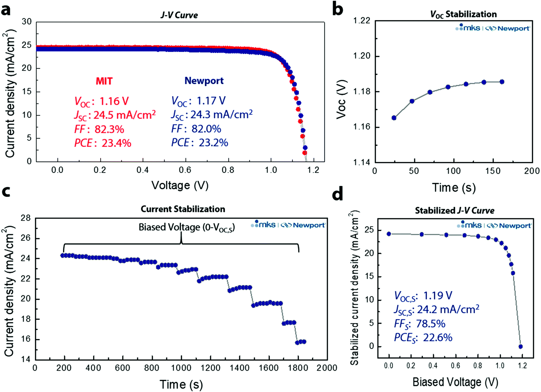 | ||
| Fig. 4 (a) 3D/LP PSC devices with efficiencies measured at MIT and at Newport. (b) Asymptotical measurement on stabilized open-circuit-voltage (VOC,S). (c) Stabilization of current density. (d) Stabilized J–V curve extracted from (b and c) with stabilized power conversion efficiency (PCES) of 22.6%. | ||
Conclusion
In summary, we have shown that the SPD strategy based on a unique combination of linear alkyl ammonium bromides and CF effectively passivates interface defects, minimizes carrier quenching, and results in a record stabilized PCE and a EL efficiency; device performance metrics that conventional surface treatment method and passivation strategies were not previously able to deliver. In addition to effectively passivating interface defects, the SPD strategy is scalable and can be combined with various printing methods that could be used for the scaled-up production of heterojunction PSCs (ink-jet printing, roll-to-roll printing, and blade coating), which inevitability employ longer contact times between the underlying perovskite layer and the solvent used for surface treatment compared to spin-coating. The SPD strategy allows for a wide processing window, providing an ideal platform for the scaled-up production of heterojunction PSCs.23Conflicts of interest
There are no conflicts to declare.Acknowledgements
J. J. Y. was funded by the Institute for Soldier Nanotechnology (ISN) grant W911NF-13-D-0001 and by the National Aeronautics and Space Administration (NASA) grant NNX16AM70H. S. N. B. was funded by the Department of Energy (DOE), Office of Basic Energy Sciences, Division of Materials Sciences and Engineering (Award Number DE-FG02-07ER46454) and through a National Science Foundation Graduate Fellowship. E. C. H. was funded through a National Defense Science and Engineering Graduate Fellowship. M. C. S. was funded by the Tata Trusts. M. R. C. was funded by the Agency for Science Technology and Research, Singapore. S. S. S., S. W., N. T. P. H., J.-P. C.-B., and T. B. were funded by NSF grant CBET-1605495, a TOTAL research grant, a U.S. Department of Energy Postdoctoral Research Award, and Skoltech 1913/R. Parts of this study were performed at the Harvard University Center for Nanoscale Systems (CNS), a member of the National Nanotechnology Coordinated Infrastructure Network (NNCI), which is supported by the National Science Foundation under NSF award no. 1541959.References
- H. J. Snaith, Nat. Mater., 2018, 17, 372–376 CrossRef CAS.
- N.-G. Park, M. Grätzel, T. Miyasaka, K. Zhu and K. Emery, Nat. Energy, 2016, 1, 16152 CrossRef CAS.
- J.-P. Correa-Baena, M. Saliba, T. Buonassisi, M. Grätzel, A. Abate, W. Tress and A. Hagfeldt, Science, 2017, 358, 739–744 CrossRef CAS PubMed.
- W. S. Yang, B.-W. Park, E. H. Jung, N. J. Jeon, Y. C. Kim, D. U. Lee, S. S. Shin, J. Seo, E. K. Kim, J. H. Noh and S. Il Seok, Science, 2017, 356, 1376–1379 CrossRef CAS PubMed.
- M. Saliba, T. Matsui, K. Domanski, J.-Y. Seo, A. Ummadisingu, S. M. Zakeeruddin, J.-P. Correa-Baena, W. R. Tress, A. Abate, A. Hagfeldt and M. Grätzel, Science, 2016, 354, 206–209 CrossRef CAS PubMed.
- M. Abdi-Jalebi, Z. Andaji-Garmaroudi, S. Cacovich, C. Stavrakas, B. Philippe, J. M. Richter, M. Alsari, E. P. Booker, E. M. Hutter, A. J. Pearson, S. Lilliu, T. J. Savenije, H. Rensmo, G. Divitini, C. Ducati, R. H. Friend and S. D. Stranks, Nature, 2018, 555, 497–501 CrossRef CAS PubMed.
- S. S. Shin, E. J. Yeom, W. S. Yang, S. Hur, M. G. Kim, J. Im, J. Seo, J. H. Noh and S. Il Seok, Science, 2017, 356, 167–171 CrossRef CAS PubMed.
- N. J. Jeon, J. H. Noh, W. S. Yang, Y. C. Kim, S. Ryu, J. Seo and S. Il Seok, Nature, 2015, 517, 476–480 CrossRef CAS PubMed.
- M. Saliba, T. Matsui, J.-Y. Seo, K. Domanski, J.-P. Correa-Baena, M. K. Nazeeruddin, S. M. Zakeeruddin, W. Tress, A. Abate, A. Hagfeldt and M. Grätzel, Energy Environ. Sci., 2016, 9, 1989–1997 RSC.
- A. Swarnkar, A. R. Marshall, E. M. Sanehira, B. D. Chernomordik, D. T. Moore, J. A. Christians, T. Chakrabarti and J. M. Luther, Science, 2016, 354, 92–95 CrossRef CAS PubMed.
- Y. Shao, Z. Xiao, C. Bi, Y. Yuan and J. Huang, Nat. Commun., 2014, 5, 5784 CrossRef CAS PubMed.
- G. S. Han, H. S. Chung, B. J. Kim, D. H. Kim, J. W. Lee, B. S. Swain, K. Mahmood, J. S. Yoo, N.-G. Park, J. H. Lee and H. S. Jung, J. Mater. Chem. A, 2015, 3, 9160–9164 RSC.
- Y. Lin, Y. Bai, Y. Fang, Z. Chen, S. Yang, X. Zheng, S. Tang, Y. Liu, J. Zhao and J. Huang, J. Phys. Chem. Lett., 2018, 9, 654–658 CrossRef CAS PubMed.
- X. Zheng, B. Chen, J. Dai, Y. Fang, Y. Bai, Y. Lin, H. Wei, X. C. Zeng and J. Huang, Nat. Energy, 2017, 2, 17102 CrossRef CAS.
- H. Tan, A. Jain, O. Voznyy, X. Lan, F. P. García de Arquer, J. Z. Fan, R. Quintero-Bermudez, M. Yuan, B. Zhang, Y. Zhao, F. Fan, P. Li, L. N. Quan, Y. Zhao, Z.-H. Lu, Z. Yang, S. Hoogland and E. H. Sargent, Science, 2017, 355, 722–726 CrossRef CAS PubMed.
- J.-K. Sun, S. Huang, X.-Z. Liu, Q. Xu, Q.-H. Zhang, W.-J. Jiang, D.-J. Xue, J.-C. Xu, J.-Y. Ma, J. Ding, Q.-Q. Ge, L. Gu, X.-H. Fang, H.-Z. Zhong, J.-S. Hu and L.-J. Wan, J. Am. Chem. Soc., 2018, 140, 11705–11715 CrossRef CAS PubMed.
- K. Lin, J. Xing, L. N. Quan, F. P. G. de Arquer, X. Gong, J. Lu, L. Xie, W. Zhao, D. Zhang, C. Yan, W. Li, X. Liu, Y. Lu, J. Kirman, E. H. Sargent, Q. Xiong and Z. Wei, Nature, 2018, 562, 245–248 CrossRef CAS PubMed.
- Y. Cho, A. M. Soufiani, J. S. Yun, J. Kim, D. S. Lee, J. Seidel, X. Deng, M. A. Green, S. Huang and A. W. Y. Ho-Baillie, Adv. Energy Mater., 2018, 1703392 CrossRef.
- M. C. Gélvez-Rueda, E. M. Hutter, D. H. Cao, N. Renaud, C. C. Stoumpos, J. T. Hupp, T. J. Savenije, M. G. Kanatzidis and F. C. Grozema, J. Phys. Chem. C, 2017, 121, 26566–26574 CrossRef PubMed.
- M. Jung, T. J. Shin, J. Seo, G. Kim and S. Il Seok, Energy Environ. Sci., 2018, 11, 2188–2197 RSC.
- Y. Hassan, Y. Song, R. D. Pensack, A. I. Abdelrahman, Y. Kobayashi, M. A. Winnik and G. D. Scholes, Adv. Mater., 2016, 28, 566–573 CrossRef CAS PubMed.
- S.-H. Turren-Cruz, M. Saliba, M. T. Mayer, H. Juárez-Santiesteban, X. Mathew, L. Nienhaus, W. Tress, M. P. Erodici, M.-J. Sher, M. G. Bawendi, M. Grätzel, A. Abate, A. Hagfeldt and J.-P. Correa-Baena, Energy Environ. Sci., 2018, 11, 78–86 RSC.
- M. Yang, Z. Li, M. O. Reese, O. G. Reid, D. H. Kim, S. Siol, T. R. Klein, Y. Yan, J. J. Berry, M. F. A. M. van Hest and K. Zhu, Nat. Energy, 2017, 2, 17038 CrossRef CAS.
- K. T. Cho, S. Paek, G. Grancini, C. Roldán-Carmona, P. Gao, Y. Lee and M. K. Nazeeruddin, Energy Environ. Sci., 2017, 10, 621–627 RSC.
- T. Zhao, C. C. Chueh, Q. Chen, A. Rajagopal and A. K. Y. Jen, ACS Energy Lett., 2016, 1, 757–763 CrossRef CAS.
- H. Tsai, W. Nie, J.-C. Blancon, C. C. Stoumpos, R. Asadpour, B. Harutyunyan, A. J. Neukirch, R. Verduzco, J. J. Crochet, S. Tretiak, L. Pedesseau, J. Even, M. A. Alam, G. Gupta, J. Lou, P. M. Ajayan, M. J. Bedzyk, M. G. Kanatzidis and A. D. Mohite, Nature, 2016, 536, 312–316 CrossRef CAS PubMed.
- D. S. Lee, J. S. Yun, J. Kim, A. M. Soufiani, S. Chen, Y. Cho, X. Deng, J. Seidel, S. Lim, S. Huang and A. W. Y. Ho-Baillie, ACS Energy Lett., 2018, 647–654 CrossRef CAS.
- N. Ahn, K. Kwak, M. S. Jang, H. Yoon, B. Y. Lee, J.-K. Lee, P. V. Pikhitsa, J. Byun and M. Choi, Nat. Commun., 2016, 7, 13422 CrossRef CAS PubMed.
- J. Ciro, S. Mesa, J. I. Uribe, M. A. Mejía-Escobar, D. Ramirez, J. F. Montoya, R. Betancur, H.-S. Yoo, N.-G. Park and F. Jaramillo, Nanoscale, 2017, 9, 9440–9446 RSC.
- P. Chen, Y. Bai, S. Wang, M. Lyu, J.-H. Yun and L. Wang, Adv. Funct. Mater., 2018, 1706923 CrossRef.
- D.-Y. Son, S.-G. Kim, J.-Y. Seo, S.-H. Lee, H. Shin, D. Lee and N.-G. Park, J. Am. Chem. Soc., 2018, 140, 1358–1364 CrossRef CAS PubMed.
- W. Tress, J. Phys. Chem. Lett., 2017, 8, 3106–3114 CrossRef CAS PubMed.
- R. B. Dunbar, B. C. Duck, T. Moriarty, K. F. Anderson, N. W. Duffy, C. J. Fell, J. Kim, A. Ho-Baillie, D. Vak, T. Duong, Y. Wu, K. Weber, A. Pascoe, Y.-B. Cheng, Q. Lin, P. L. Burn, R. Bhattacharjee, H. Wang and G. J. Wilson, J. Mater. Chem. A, 2017, 5, 22542–22558 RSC.
- E. Zimmermann, K. K. Wong, M. Müller, H. Hu, P. Ehrenreich, M. Kohlstädt, U. Würfel, S. Mastroianni, G. Mathiazhagan, A. Hinsch, T. P. Gujar, M. Thelakkat, T. Pfadler and L. Schmidt-Mende, APL Mater., 2016, 4, 091901 CrossRef.
- L. Wagner, S. Chacko, G. Mathiazhagan, S. Mastroianni and A. Hinsch, ACS Energy Lett., 2018, 1122–1127 CrossRef CAS.
- M. Saliba, Science, 2018, 359, 388–389 CrossRef CAS PubMed.
Footnote |
| † Electronic supplementary information (ESI) available. See DOI: 10.1039/c9ee00751b |
| This journal is © The Royal Society of Chemistry 2019 |