
 Open Access Article
 This Open Access Article is licensed under a
 Creative Commons Attribution 3.0 Unported Licence
Stable and tunable phosphonic acid dipole layer for band edge engineering of photoelectrochemical and photovoltaic heterojunction devices†
René
Wick-Joliat
 a,
Tiziana
Musso
a,
Rajiv Ramanujam
Prabhakar
a,
Johannes
Löckinger
b,
Sebastian
Siol
b,
Wei
Cui
a,
Laurent
Sévery
a,
Thomas
Moehl
a,
Jihye
Suh
a,
Jürg
Hutter
a,
Marcella
Iannuzzi
a and
S. David
Tilley
*a
a,
Tiziana
Musso
a,
Rajiv Ramanujam
Prabhakar
a,
Johannes
Löckinger
b,
Sebastian
Siol
b,
Wei
Cui
a,
Laurent
Sévery
a,
Thomas
Moehl
a,
Jihye
Suh
a,
Jürg
Hutter
a,
Marcella
Iannuzzi
a and
S. David
Tilley
*a
aDepartment of Chemistry, University of Zurich, Winterthurerstrasse 190, CH-8057 Zürich, Switzerland. E-mail: david.tilley@chem.uzh.ch
bEmpa – Swiss Federal Laboratories for Materials Science and Technology, Überlandstrasse 129, CH-8600 Dübendorf, Switzerland
First published on 26th April 2019
Abstract
A key challenge for photoelectrochemical water splitting is that high performance semiconductors are not stable in aqueous electrolytes, necessitating corrosion protection layers such as TiO2. In the best case, the protection layer would also serve as the heterojunction partner, minimizing complexity and thereby cost. However, the bands of most high performance semiconductors are poorly aligned with TiO2, limiting the photovoltage. Here, we describe a method to overcome this limitation through the placement of a tunable dipole layer at the interface of the p- and n-type materials, shifting the relative band positions to enable an increased photovoltage. The introduction of a phosphonic acid (PA, H3PO3) layer increases the photovoltage of TiO2-protected Si, Sb2Se3, and Cu2O photocathodes. The dipole effect scales with PA surface coverage, and gives even larger shifts when multilayers are employed. By varying the thickness from submonolayer to multilayer (up to 2 nm), we are able to tune the photovoltage of p-Si/TiO2 over a range of 400 mV.
Broader contextWhile usage of solar energy offers many benefits, one of its main limitations for large scale implementation is that solar irradiation varies strongly with day/night and summer/winter cycles. Efficient storage of solar energy is therefore of crucial importance, with one possibility being to convert solar energy into chemical energy, for example in the form of H2 obtained from splitting water (2H2O → 2H2 + O2). Water splitting could be achieved by coupling photovoltaic (PV) cells to an electrolyzer or, in a more direct way, in a photoelectrochemical (PEC) cell, which absorbs sunlight and, instead of generating electricity, uses the solar energy to drive a chemical reaction. PEC cells are operated in direct contact with corrosive electrolytes and measures have to be taken to protect the otherwise unstable materials. Finding suitable protection strategies is an open challenge, since not only the stability is important, but also the energetics of the protective materials have to be matched with the photoabsorbing semiconductor. This study presents a general method to tune the band alignment between photoabsorbers and one of the most promising protective materials, TiO2, which makes otherwise unfavorable material combinations more efficient. |
The maximum possible photovoltage of photoelectrochemical (PEC) cells as well as heterojunction-based photovoltaic (PV) devices is determined by the band alignment of the involved materials. In traditional PEC, the maximum photovoltage is set by the difference of the Fermi level of the semiconductor and the redox potential of the solution, while in PV the maximum theoretical photovoltage is set by the difference of the Fermi levels of the p- and n-type materials. Furthermore, large discontinuities (i.e. spikes) in the conduction band have to be avoided to assure an unhindered flow of the photo-excited electrons through the junction. Optimizing band alignments at semiconductor heterointerfaces is a key challenge in the development of new technologies for PEC and PV applications.1 Strategies to improve the band alignments include graded interfaces,2 introduction of buffer layers,3,4 doping of the electron acceptor material5 as well as interface and bulk defect engineering.6,7 However, most of these solutions are specific for a particular materials combination. An elegant way to tune the band alignment in a more general fashion is by adding a dipole layer at the junction interface, which results in an increase of band bending, minimizing recombination losses at the interface.8
The interface dipole strategy has been successfully demonstrated in the fields of organic PV,9–12 perovskite PV13,14 and quantum dot PV, utilizing self-assembled monolayers (SAMs) of carboxylic- and phosphonic acids.15–17
In traditional PEC, the dipole layer is added at the semiconductor/electrolyte interface, which usually leads to very limited stability and only a small voltage increase due to shielding of the dipole by the electrolyte.18–21 In order to compete with commercially well-established PV coupled with electrolyzers, PEC systems have to be stable for years, likely in extreme pH electrolytes.22 Thus, corrosion protection layers have been investigated, using chemically stable materials such as TiO2.23 The use of overlayers in PEC systems creates a “buried junction”, which functions much like a PV heterojunction, and therefore strategies to improve the performance of buried junction PEC cells are directly translatable to PV devices.
TiO2 is a good candidate for a protective overlayer due its chemical stability over a wide range of pH, and it has been shown to protect photoanodes as well as photocathodes.23 In the best case, TiO2 would also serve as the heterojunction partner, minimizing the number of layers in the device (i.e. the complexity) and therefore the cost. However, the band alignment of most high performance photoabsorbers (such as Si) with TiO2 is unfavorable. Thus, a dipole induced band shifting can give a better band alignment, increased photovoltage and therefore higher efficiency from these otherwise unfavorable photoabsorber/protective layer pairs.
We sought to find a dipole strategy for PEC water splitting that fulfills the following requirements: utilizes cheap and abundant materials; enables a large, tunable photovoltage increase; exhibits high stability; and is generally applicable to many different photoabsorber materials. Here, we report our strategy fulfilling the above requirements and serving as a proof of concept using p-Si as a well-behaved model photoabsorber, which would in a next step be replaced by emerging thin film materials. There is also a large body of literature on dipole modification of Si to tune its electronic properties, but those works chemically modify the Si directly and the obtained results are not transferrable to other photoabsorbing substrates.24–28
A 0.5 nm Al2O3 anchoring layer allows us to use different photoabsorbers with no changes in the dipole binding, since the dipole is deposited onto the anchoring layer and not directly onto the photoabsorber. After assessing several oxide materials (Fig. S1 and S2, ESI†), we found that Al2O3 performed best as anchoring layer and is straight-forward to deposit homogeneously in well-defined thicknesses by atomic layer deposition (ALD). Phosphonic acid (PA, H3PO3) serves as the dipole layer. In contrast to previous work using SAMs, we chose to use the spin coating technique to deposit the dipole layer which allowed us to tune the thickness of the layer without being restricted to a monolayer as maximal surface coverage. Upon screening of different phosphonic acids with different thicknesses (ranging from sub-monolayer to multilayers) in our system, the largest dipole effect was obtained using 1–2 nm of PA, where photovoltage shifts of close to 400 mV were obtained for the p-Si/TiO2 heterojunction. TiO2 was used as heterojunction partner and protective layer.
Water splitting electrodes were fabricated by depositing a platinum catalyst on the TiO2 surface. Additionally, we fabricated PV cells by sputtering a transparent conducting oxide (TCO) front contact on top of the TiO2. Qualitative band diagrams of p-Si/n-TiO2 as well as p-Si/anchor layer/PA/n-TiO2 are shown in Fig. 1A–C. The effect of the dipole is represented as a step in the vacuum energy (Evac), shifting the bands of p- and n-type layers relative to each other, and resulting in an increased band bending and photovoltage (Vph). Fig. S3 (ESI†) shows band diagrams in flat band condition, in equilibrium and under illumination for both p-Si/n-TiO2 and p-Si/anchor layer/PA/n-TiO2. The PA modification strategy was also extended to other emerging photocathodes like Sb2Se3 and Cu2O resulting in improvements in the onset potential, demonstrating the universal applicability of our approach.
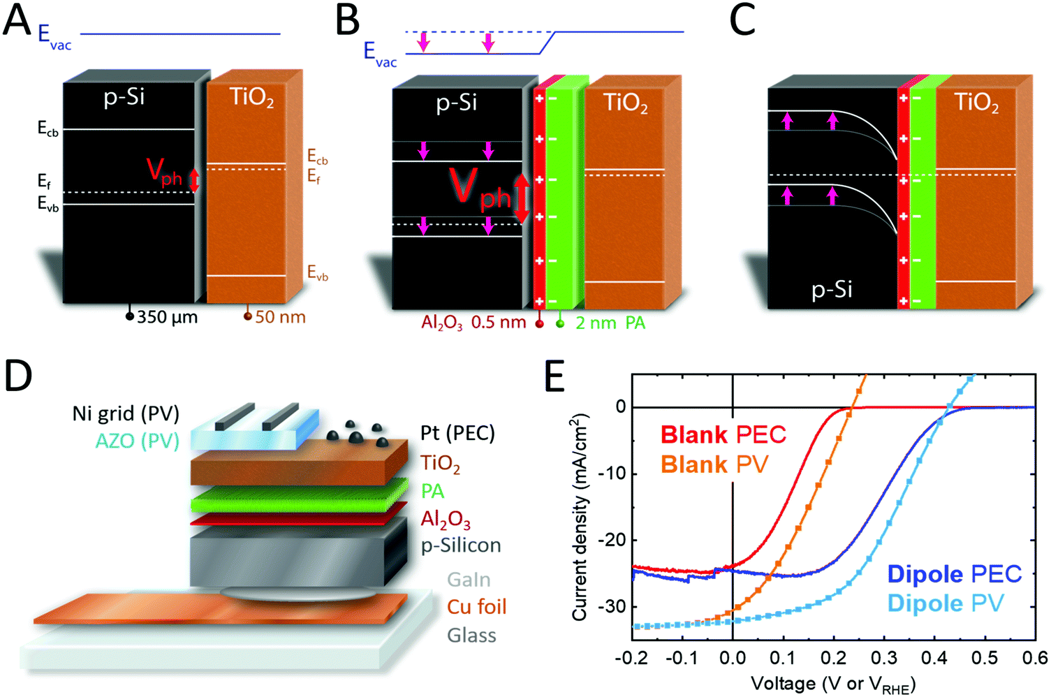 | ||
| Fig. 1 (A and B) Band diagrams of p-Si/n-TiO2 and p-Si/anchor layer/PA/n-TiO2 in flat band condition, and (C) in equilibrium, showing the increased band bending that is obtained with a dipole layer. The dipole layer induces a shift in the band edge, represented by a step in the vacuum energy level (Evac), and therefore higher photovoltage (Vph) can be obtained. Due to the high doping of TiO2, band bending in the TiO2 was omitted. (D) Device architecture of the PV and PEC cells used in this study. (E) Current density–Voltage plots of PV and PEC cells made from p-Si/n-TiO2 well as p-Si/anchor layer/PA/n-TiO2. PEC measurements in 1 M H2SO4 and 1 sun illumination, PV measurements under 1 sun illumination. The small current fluctuations in the blue trace (and other J–V curves in this paper) are attributed to the formation and release of hydrogen bubbles on the device surface. | ||
Band edge engineering at p-Si/n-TiO2 heterojunctions
The schematic structure of the dipole modified PEC and PV cells is shown in Fig. 1D. Detailed experimental methods can be found in the ESI.† Briefly, thin Al2O3 layers were deposited by ALD onto etched p-Si wafers, followed by spin coating of phosphonic acid (PA). The samples were then annealed at 120 °C in air and thoroughly rinsed with ethanol, resulting in PA layers of 0.5–2 nm thickness depending on the PA concentration used for spin coating (as determined by ellipsometry). The presence of PA on the surface was confirmed by XPS, with phosphorus core level emissions occurring at binding energies of 134.2, 135.0 and 192.0 eV (P 2p3/2, P 2p1/2, P 2s), which are in good agreement with literature reference values (Fig. S4, ESI†).29 SEM-EDX and AFM showed that the morphology of the samples did not change upon PA modification, since PA is deposited as a flat and homogeneous film. A weak phosphorus signal was detected in EDX measurement in a concentration close to the detection limit of the device (0.2–0.3 at%) (Fig. S5 and S6, ESI†). The anchoring of PA is only stable under acidic conditions. Therefore, a pH 11 solution was used to fully remove the PA layer from the substrate and the resulting PA solution was analyzed with high resolution ESI-MS, showing that PA did not undergo chemical changes during annealing and was still present as H3PO3 (Fig. S7, ESI†). PA diffraction peaks were not observed in XRD measurements due to the very thin nature of the PA layer.In a next step, n-TiO2 was deposited on p-Si/Al2O3/PA samples by ALD. We have previously shown that ∼50 nm of ALD-TiO2 is sufficient to minimize the chance of a pinhole over larger areas (1 cm2),30 thus 50 nm TiO2 was used in this work. PEC devices were then fabricated by sputtering 1 nm of Pt as hydrogen evolving catalyst,31 and PV cells were fabricated by sputtering 200 nm aluminum-doped zinc oxide (AZO) followed by a 4 μm Ni grid as a front contact.32Fig. 1E shows current density–voltage plots for p-Si/n-TiO2 PEC cells and PV devices. By introducing an anchor layer and a PA layer at the interface of the p-Si and n-TiO2, the J–V curves are shifted to higher potentials by 200 mV (Fig. 1E, blue traces). This shift leads to an increased Voc and a higher fill factor (FF), and a power conversion efficiency (PCE) increase by more than 100% (figures of merit for PEC and PV in Tables S1 and S2, ESI†). The measured Jsc values are confirmed by the external quantum efficiency (EQE) spectra, giving an integrated current density of 31.6 mA cm−2 (Fig. S8, ESI†) for the solar cells. p-Si/TiO2 PEC devices have been reported in the literature and hardly exceed photovoltages of 200 mV, in agreement with our blank samples lacking the dipole stack.28,33 The high photovoltage that we obtain with the p-Si/Al2O3/PA/TiO2 heterojunction can usually only be obtained with homojunction Si.
We attribute the increased photovoltages in the PA modified devices to a dipole effect caused by the covalent binding of the PA layer onto the anchor layer metal oxide (in most cases Al2O3, which gives the highest performance devices, but TiO2 and Ga2O3 and even native SiO2 showed the same band shifting behavior; Fig. S1, ESI†). These anchor layers were grown by ALD and are naturally OH terminated.34 Replacement of the hydroxyl groups by phosphonate groups, which are more electron withdrawing, gives a surface dipole that results in a downward shift of the substrate bands. The dipole magnitude increases linearly with increasing surface coverage, as more and more electron donating hydroxyl groups are replaced by electron withdrawing phosphonate groups (Fig. S9, ESI†).
DFT simulations have been employed to model the anchor layer/PA interface. A variety of different binding modes of PA to TiO2 were proposed in the literature, ranging from monodentate35 to bidentate.36,37 An analysis of the adsorption modes of one PA molecule on a specific bulk-like TiO2 slab, where the PA molecules are mirrored on the bottom side to avoid spurious dipole effects, results in the bidentate B2 mode as the most stable one (Fig. 2 and Fig. S10, ESI†). The TiO2 anchor layer that was used in a subset of devices has been modeled with a three layers thick rutile TiO2(110) slab, where the surface has been terminated with hydroxyl groups38 while the bottom side has been passivated with hydrogens. The presence of OH groups on ALD grown TiO2 surfaces is evident from the ALD growth mechanism and was also demonstrated experimentally.34,39,40
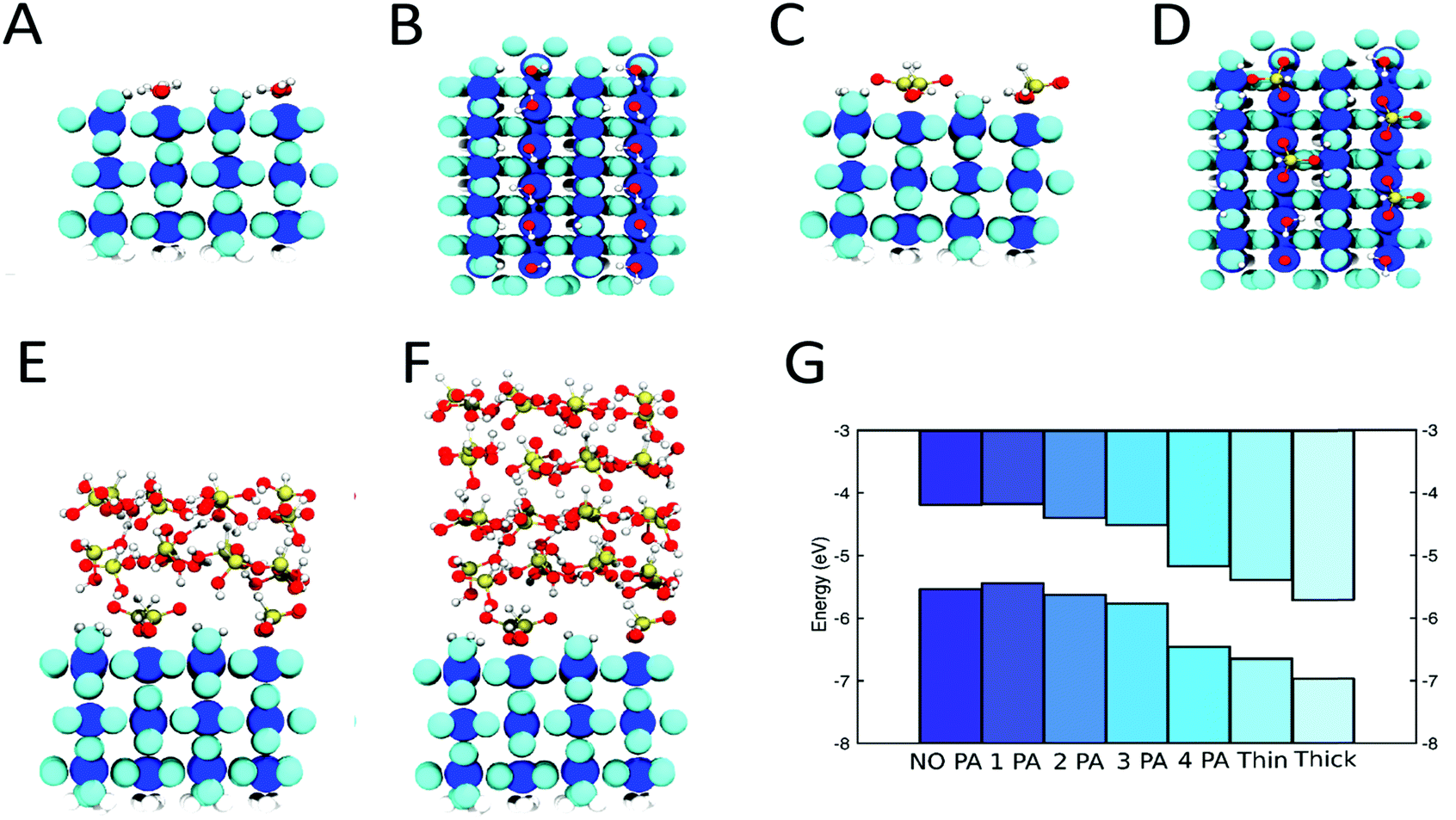 | ||
| Fig. 2 Optimized configurations of hydroxylated TiO2 (A and B) and TiO2/PA with maximum PA coverage (C and D), TiO2 with a thin PA multilayer (E) and thick PA multilayer (F). Color code: blue atoms represent Ti, cyan atoms the O of TiO2, red is for O, gold for P and white for H. All TiO2 atoms are enlarged for clarity purposes. (G) Bands alignment (top: conduction band, bottom: valence band) for different coverages of PA on TiO2, namely from left to right: fully hydroxylated TiO2, TiO2 with 1, 2, 3 and 4 PA molecules adsorbed on top as well as TiO2 with a thin and thick PA multilayer. The bands are shifted downwards with increasing PA coverage. | ||
Increasing PA surface coverage was modeled by sequentially placing additional PA molecules onto the hydroxylated TiO2 until a full PA monolayer coverage was obtained (Fig. 2C and D). To model our experimental findings of up to 2 nm thick PA layers, we started with a TiO2 substrate with full PA monolayer coverage and added a crystalline PA layer,41 which was slightly strained to match the TiO2 substrate and then equilibrated for a few picoseconds at 300 K with ab initio molecular dynamics simulations. Two and four layers of PA were added on top of the first PA monolayer to simulate PA layer thicknesses of approximately 1 and 2 nm (Fig. 2E and F).
Fig. 2G shows the calculated band structures with increasing PA coverage, where the band alignment has been obtained from macroscopic-averaged wavefunction values (Computational details in ESI†). The bands are shifted to more negative energy values on the vacuum scale (or to more positive values on the RHE scale) as more PA molecules are adsorbed on TiO2(110). In our simulations, the shift increases even more, as we go from a full PA monolayer to a multilayer, which is in good agreement with our experimental results. The origin of this multilayer effect seems to arise from the restructuring at the interface of the PA that is covalently bound to the TiO2 with the annealed PA layer. The magnitude of the calculated band shift is larger than the experimentally determined Vonset shift since surface states of the photoabsorber are expected to limit the obtainable shift as discussed below. Furthermore, in real devices, the electrolyte or the TiO2 protection layer may shield and therefore reduce the observed shift. Those factors were not accounted for in our calculations. Nevertheless, we conclude that a three layer thick TiO2(110) slab is an appropriate model for the amorphous TiO2 anchor layers obtained by ALD and the qualitative results (direction of the dipole as well as the trend with increasing PA surface coverage) can be extended to other metal oxide anchor layers.
In addition to DFT calculations, several experimental results support the dipole hypothesis. XPS measurements revealed that PA modification of p-Si/Al2O3 leads to an increase in band bending (i.e. shifting of the band edge). Core level emissions corresponding to the Al2O3 anchor layer (Al 2p) as well as the native SiO2 layer (Si 2p) exhibit a much stronger shift in binding energies than the core level emission associated with pure Si, indicating an increase in band bending on the order of 0.5 eV in the surface region of the PA modified p-Si/Al2O3 sample (Fig. S11, ESI†).
We also carried out the PA modification experiment on n-type silicon as well as p–n junction silicon. It has been demonstrated that relatively thick (>100 nm) ALD TiO2 layers coated with a nickel catalyst are indeed conductive for photo-generated holes by an underlying n-type silicon photoabsorber.42 As expected, the samples fabricated with n-type silicon also exhibit a band shift leading to a later Vonset and decreased Voc by 200–250 mV (Fig. S12 and S13, ESI†). On the other hand, when p–n silicon was coated with PA, we did not observe any change in Voc or Vonset, since the photovoltage is generated inside the p-Si/n-Si homojunction and not affected by a dipole layer stacked outside that junction (Fig. S14 and S15, ESI†). The finding that a PA layer shifts the onset potentials to more positive values on p-Si/TiO2 photocathode as well as n-Si/TiO2 photoanode but does not affect the pn-Si/TiO2 photocathode strongly supports the dipole hypothesis.
We note that the dipole as drawn in Fig. 1B and Fig. S9 (ESI†) is pointing in the opposite direction of the molecular gas phase dipole of PA. In our devices the dipole is rather formed by a difference in electron withdrawing/donating behavior of phosphonate as compared to hydroxyl surface termination of the anchor layer, and the gas phase dipole of the PA appears to be one out of multiple minor factors influencing the magnitude of the observed shift.43 Therefore, substituted phosphonic acids on an anchor layer should also give a similar dipole as PA despite having substantially different gas phase dipole moments. This hypothesis was tested by fabricating PEC devices with fluorophosphonic acid (dipole moment = −1.1 D), phosphoric acid (0.0 D), hydroxybenzylphosphonic acid (+4.8 D), methylphosphonic acid (+0.6 D) instead of PA (−0.3 D). All of these samples showed an increased photovoltage as compared to a blank sample without dipole layer (Fig. S16, ESI†).
In agreement with the DFT calculations, we found that the increase in Voc in p-Si/Al2O3/PA/TiO2 samples scaled with PA thickness and thus with PA concentration used in the spin coating step. The dipole magnitude increases even more as we go from a full monolayer to a multilayer (2 nm PA ≈ 4–5 monolayers). Exploiting PA thickness dependence, we were able to fine tune the Vonset from +0.07 VRHE up to +0.48 VRHE over a range of 410 mV (Fig. 3A). A maximum Vonset shift of 410 mV was obtained with PA concentrations of 20 mM (giving rise to a ∼2 nm thick layer, as measured by ellipsometry). Thicker PA layers affect the series resistance of the device, leading to a decrease in the performance for PA concentrations greater than 50 mM. Samples made with PA concentrations of 10 and 20 mM (1.5–2 nm thick) showed the highest performance with good Vonset increase while retaining low series resistance (Fig. 3B).
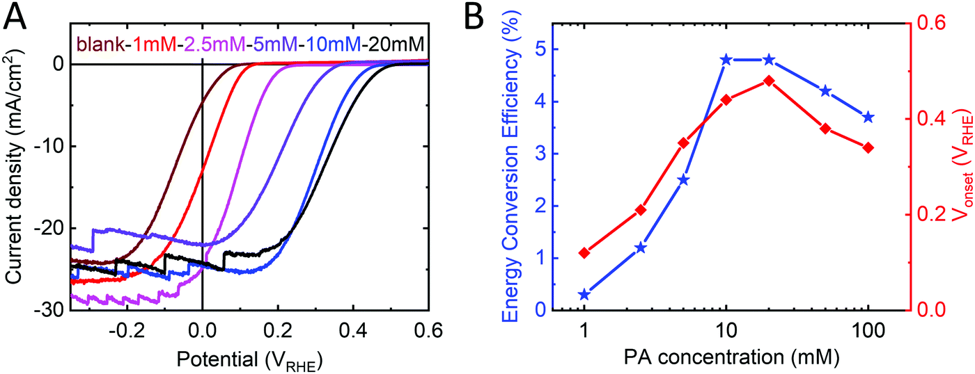 | ||
| Fig. 3 (A) Current density–voltage plots of PEC devices with the structure p-Si/Al2O3/PA/TiO2/Pt with different PA concentrations used for spin coating of the dipole layer (maroon: no dipole layer; black: 20 mM PA). Linear sweeps were recorded in 1 M H2SO4 and 1 sun illumination at scan speed of 10 mV s−1. (B) Dependence of energy conversion efficiency and onset potential (Vonset) on the PA concentration used to make the dipole layer. | ||
Our measurements show that the PA layer is not stable in direct contact with the electrolyte (Fig. S17, ESI†) and even changes its morphology when kept unprotected in air for more than a day (presumably due to a slow dewetting process, Fig. S18, ESI†). However, when protected from the electrolyte by a TiO2 overlayer, the PA layer does not limit the stability of the device. The Vonset shift is stable for more than 2 h in 1 M H2SO4, under 1 sun illumination and at 0 VRHE (Fig. 4A). The J–V curve after stability measurement even shows a small increase in photovoltage for both types of devices (PEC and PV). After prolonged illumination, both the blank sample as well as the dipole-modified sample start to degrade and gradually lose their performance. This phenomenon has been previously demonstrated and is attributed to detachment of the Pt catalyst particles followed by TiO2 corrosion as soon as the accumulated electrons cannot be transferred into the electrolyte and degrade the TiO2 instead.44
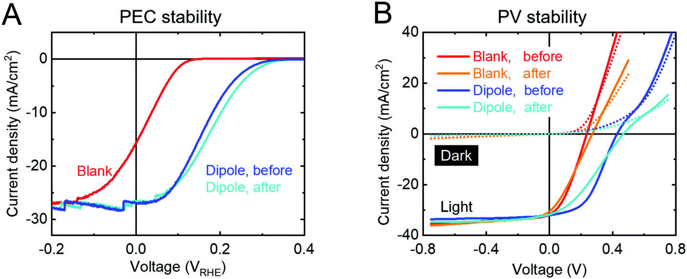 | ||
| Fig. 4 (A) Current density–voltage curves of a p-Si/Al2O3/PA/TiO2/Pt sample before (blue) and after (light blue) a 2 hour chronoamperometry measurement at 0 VRHE in 1 M H2SO4 under 1 sun illumination. A linear sweep measurement of the blank sample p-Si/TiO2/Pt (red) is also included. (B) Current density–voltage plots of PV cells in the dark (dotted lines) and under 1 sun illumination (solid lines) before and after heat soaking at 80 °C and 1 sun illumination with max power point tracking for 6 days in N2 atmosphere. | ||
The stability of the PV devices was tested by keeping them at 80 °C under 1 sun illumination at the maximum power point for 6 days (Fig. 4B). After 6 days of this treatment, all devices (with and without dipole) showed a Voc increase by 40 mV, unchanged Jsc and smaller FF. Obviously, the dark currents (dotted lines, Fig. 4B) of all samples decreased upon stability measurements, indicating an increased series resistance that causes the FF decreases under illumination. There are numerous possible reasons for such an increase in the series resistance (e.g. front- and back contacts). Fig. S19 (ESI†) shows how the figures of merit develop over time during the stability measurements and indicate that all major changes take place in the first few hours of the measurement before reaching a very stable equilibrium state. One of these stabilization processes even leads to a slightly increased Voc, but since this effect is also observed in the blank p-Si/TiO2 samples, it is not directly related to the dipole layer and was not further investigated in this study. S-Shaped J–V curves have been observed in several solar cell device types like OPV and CIGS.45,46 Such behavior can be explained by the mismatch of the bands at a heterojunction, which may indicate that we have reached the limit of Voc maximation for this heterojunction. We can conclude, however, that the dipole layer is not limiting the stability of the device.
The built-in voltage of the p-Si/n-TiO2 PV cells was determined using Mott–Schottky analysis with data obtained from electrical impedance spectroscopy. The p-type doping of the silicon wafer is evident from the plot of the inverse of the squared space charge capacitance (1/C2) versus applied potential (Fig. 5). It is observed that the PA dipole layer shifts the flat band potential (EFB) of the device from 0.22 V to 0.49 V, which is in good agreement with the increased Voc (Fig. 1E). A very similar difference in EFB was also observed when bare ALD-TiO2 on FTO glass was modified with a PA layer, with and without protection by a second (very thin, 2 nm) TiO2 layer. Those samples showed an EF shift of 200–300 mV upon PA modification, depending upon whether a second TiO2 layer was employed, which partially shielded the dipole effect of the PA and led to smaller EFB shifts (see Fig. S20, ESI† for discussion).
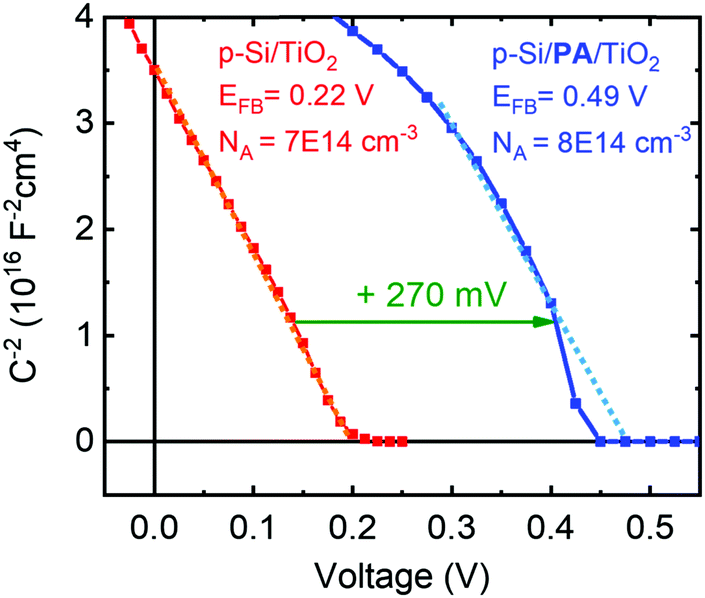 | ||
| Fig. 5 Mott–Schottky analysis of p-Si/TiO2 and p-Si/Al2O3/PA/TiO2 PV cells obtained from impedance measurements in the dark. Experimental and fitting details are given in the ESI.† The measured doping densities match with the resistivity data provided by the manufacturer. | ||
Improvement of emerging material thin film devices
We sought to demonstrate the versatility of this dipole approach by applying it to emerging thin film materials. Two potential candidates under study in our group, Sb2Se3 and Cu2O, showed an improved performance and onset potential when a dipole layer was spin coated onto the photoabsorber prior to deposition of the protecting layer and n-type heterojunction partner, TiO2 (Fig. 6). Sb2Se3 has shown high efficiencies in PV (9.2%)47 and our group has reported very high PEC current densities of 16 mA cm−2 using Sb2Se3 with MoSx catalyst for hydrogen evolution.48 However, energy conversion efficiencies are limited by poor photovoltages. Modifying Sb2Se3 with a thin TiO2 anchor layer and PA dipole layer followed by protection with 50 nm ALD TiO2 increased the photovoltage by 40 mV as compared to the blank sample without the dipole layer (Fig. 6A) resulting in Sb2Se3 devices reaching a thermodynamically-based energy conversion efficiency over 1% (Fig. 6B) with onsets comparable to the very best reports in the literature.49–51 Furthermore, the large dark current observed in the Sb2Se3/TiO2 device is suppressed when a dipole layer is utilized (Fig. 6A, dotted lines).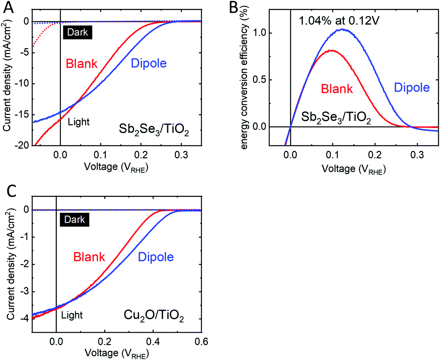 | ||
| Fig. 6 (A) Current density–voltage plots of Sb2Se3/TiO2 (red) and Sb2Se3/TiO2/PA/TiO2 (blue). Linear sweeps were recorded in 1 M H2SO4 at a scan speed of 10 mV s−1 in the dark (dotted) and under 1 sun illumination (solid). (B) Energy conversion efficiency of the same devices. (C) Current–voltage plots of Cu2O/TiO2 (red) and Cu2O/TiO2/PA/TiO2 (blue). Linear sweeps were recorded in 1 M phosphate solution at pH 7 at a scan rate of 10 mV s−1 in the dark (dotted) and under 1 sun illumination (solid). | ||
For cuprous oxide,52 we spin coated PA onto electrodeposited Cu2O covered with a 1 nm TiO2 anchor layer and protected the PA with 50 nm ALD TiO2. These samples showed a photovoltage increase by 70 mV as compared to the blank samples without PA layers. Vonset of the blank samples (0.4 VRHE) are in line with values reported for p-Cu2O/TiO2 heterojunction PEC cells,53,54 while Vonset of our dipole modified samples (0.5 VRHE) sets a new record photovoltage for this heterojunction in PEC water splitting.
It should be noted that the choice of the anchor layer and PA spin coating conditions require optimization for each substrate. In the p-Si/n-TiO2 system, we found that Al2O3 is the ideal anchor layer while Sb2Se3 and Cu2O worked best with TiO2 as anchor layer. We hypothesize that more large band gap metal oxide materials could serve this purpose and for some materials even the native oxide layer forming on the semiconductor surface could serve as an anchor layer. As an example, Fig. S1 (ESI†) compares the influence of different anchor layers (Al2O3, Ga2O3, TiO2, native SiO2) on the performance of p-Si/anchor layer/PA/n-TiO2 devices. Furthermore, the behavior of PA during the spin coating process is strongly influenced by the surface morphology of the substrate. Using relatively high PA concentrations of 10–20 mM were ideal to form a nanometer thick PA film on perfectly flat Si substrate, giving large photovoltage improvement while still maintaining a low series resistance. On the other hand, for Sb2Se3 as well as Cu2O, both of which feature a rougher surface, high PA concentrations gave very resistive devices and therefore decreased performance as compared to blank samples. For those materials the ideal PA thickness was obtained using a concentration of 1–2 mM PA giving a large photovoltage shift and low series resistance.
It should also be emphasized that for some substrates the photovoltage is limited by Fermi level pinning due to a high density of surface states within the band gap of the material. In those cases the photovoltage is independent of the band alignment with the heterojunction partner and also a dipole (for example the PA layer reported herein) will not lead to an increased photovoltage.55 Therefore, if the anchor layer itself does not passivate the surface states well enough, additional steps are required to passivate the surface states before a dipole layer is added. In a few cases partial Fermi level pinning was also reported and those substrates would show an increased photovoltage upon addition of a dipole layer, but the increase is expected to be much smaller than in an unpinned system and we assume this to be the reason for the smaller Vonset shifts observed for Cu2O and Sb2Se3 substrates as compared to p-Si.56 To unravel whether the lack of a photovoltage increase can be attributed to a very weak dipole or to Fermi level pinning, work function measurements (by ultraviolet photoelectron spectroscopy (UPS) or Kelvin probe force microscopy (KPFM)) can be used to clarify the presence or absence of a dipole, since the dipole has an effect on the work function even if the Fermi level is pinned and is therefore “invisible” in (photo)electrochemical measurements.55
Conclusion
We have shown that inorganic, molecular phosphonic acid layers can be used as interface dipole layers to increase the photovoltage of several heterojunctions employed for photoelectrochemical (PEC) water splitting. The strategy was developed on a p-Si/n-TiO2 system, where TiO2 functioned as both the heterojunction partner and as a corrosion protective layer, enabling us to fabricate PV cells and PEC cells by only exchanging the front contact/catalyst. A large increase in photovoltage was observed (+200 mV), with excellent stability, which was not limited by the dipole layer in both the PV and PEC devices. The PA layer thickness depends on the PA concentration used in spin coating and enables the fine-tuning of the band shift in a range of 0–400 mV. DFT calculations and experimental methods (XPS, electrochemical impedance) were employed to support our hypothesis that the dipole is formed at the anchor layer/PA interface by replacing the natural OH surface termination by functional groups with different electron donating/withdrawing behavior. Furthermore, a PA multilayer increases the dipole even more than a monolayer, due to some slight structural changes at the anchor layer/PA interface induced by the PA network. Insertion of a PA layer in Sb2Se3/TiO2 and Cu2O/TiO2 allowed us to increase the photovoltage by 40 and 70 mV, respectively, demonstrating the versatility of our approach.Author contributions
R. W. J. and S. D. T. conceived the project, directed the experiments and analyzed the data. R. W. J. fabricated the samples, carried out electrochemical and SEM measurements and wrote the manuscript. J. L. fabricated and tested the PV devices. T. Musso performed the DFT calculations, T. Musso, M. J. and J. H. planned the DFT calculations and analyzed the results. S. S. performed XPS and AFM measurements. R. R. P. provided the Sb2Se3 substrates and W. C. synthesized the Cu2O samples. J. S. performed XRD measurements. T. Moehl assisted with EIS measurements. L. S. assisted with the characterization of the devices. All authors contributed to data analysis, read and commented on the manuscript.Conflicts of interest
There are no conflicts to declare.Acknowledgements
This research was funded by the Swiss National Science Foundation, AP Energy Grant # PYAPP2 160586, and the University of Zurich Research Priority Program (URPP) LightChEC. Sebastian Siol acknowledges funding from COST project IZCNZ0-174856 C16.0075, in the COST Action MP1407 (e-MINDS). For computing resources, we thank the Swiss National Supercomputer Centre (CSCS) under the projects ID s657 and uzh1. The authors acknowledge the assistance and support of the Center for Microscopy and Image Analysis at the University of Zurich for help with SEM characterization as well as the Mass Spectrometry service at University of Zurich for HR-ESI-MS measurements. We also want to thank Dr. Claudia Cancellieri for her help with AFM measurements, and Prof. Jürg Osterwalder and Dr Yaroslav E. Romanyuk for valuable discussions.References
- W. Jaegermann, A. Klein and T. Mayer, Adv. Mater., 2009, 21, 4196–4206 CrossRef CAS.
- J. Fritsche, A. Klein and W. Jaegermann, Adv. Eng. Mater., 2005, 7, 914–920 CrossRef CAS.
- C.-H. M. Chuang, P. R. Brown, V. Bulović and M. G. Bawendi, Nat. Mater., 2014, 13, 796–801 CrossRef CAS PubMed.
- T. Minami, Y. Nishi and T. Miyata, Appl. Phys. Express, 2013, 6, 044101 CrossRef.
- S. E. Shaheen, W. J. Mitchell, M. F. A. M. van Hest, R. T. Collins, D. C. Olson, M. S. White and D. S. Ginley, Adv. Funct. Mater., 2006, 17, 264–269 Search PubMed.
- S. Siol, J. C. Hellmann, S. D. Tilley, M. Graetzel, J. Morasch, J. Deuermeier, W. Jaegermann and A. Klein, ACS Appl. Mater. Interfaces, 2016, 8, 21824–21831 CrossRef CAS PubMed.
- X. Yan, Q. Liang, S. Cao, Y. Zhang, Z. Kang and X. Liao, Nano Energy, 2016, 24, 25–31 CrossRef.
- R. E. Brandt, M. Young, H. H. Park, A. Dameron, D. Chua, Y. S. Lee, G. Teeter, R. G. Gordon and T. Buonassisi, Appl. Phys. Lett., 2014, 105, 263901 CrossRef.
- S. Khodabakhsh, B. M. Sanderson, J. Nelson, T. S. Jones, J. S. Kim, J. H. Park, J. H. Lee, J. Jo, D. Kim, K. Cho, J. S. Kim, J. H. Park, J. H. Lee, J. Jo and D. Kim, Adv. Funct. Mater., 2006, 16, 95–100 CrossRef CAS.
- C. Goh, S. R. Scully and M. D. McGehee, J. Appl. Phys., 2007, 101, 1–12 CrossRef.
- J. S. Kim, J. H. Park, J. H. Lee, J. Jo, D. Y. Kim and K. Cho, Appl. Phys. Lett., 2007, 91, 1–4 Search PubMed.
- H. Ma, H.-L. Yip, F. Huang and A. K.-Y. Jen, Adv. Funct. Mater., 2010, 20, 1371–1388 CrossRef CAS.
- L. Zuo, Z. Gu, T. Ye, W. Fu, G. Wu, H. Li and H. Chen, J. Am. Chem. Soc., 2015, 137, 2674–2679 CrossRef CAS PubMed.
- Y. C. Shih, L. Y. Wang, H. C. Hsieh and K. F. Lin, J. Mater. Chem. A, 2015, 3, 9133–9136 RSC.
- G. H. Kim, F. P. García De Arquer, Y. J. Yoon, X. Lan, M. Liu, O. Voznyy, Z. Yang, F. Fan, A. H. Ip, P. Kanjanaboos, S. Hoogland, J. Y. Kim and E. H. Sargent, Nano Lett., 2015, 15, 7691–7696 CrossRef CAS PubMed.
- R. Azmi, S. Y. Nam, S. Sinaga, S. H. Oh, T. K. Ahn, S. C. Yoon, I. H. Jung and S. Y. Jang, Nano Energy, 2017, 39, 355–362 CrossRef CAS.
- R. Azmi, H. Aqoma, W. T. Hadmojo, J. M. Yun, S. Yoon, K. Kim, Y. R. Do, S. H. Oh and S. Y. Jang, Adv. Energy Mater., 2016, 6, 1–10 Search PubMed.
- U. Koldemir, J. L. Braid, A. Morgenstern, M. Eberhart, R. T. Collins, D. C. Olson and A. Sellinger, J. Phys. Chem. Lett., 2015, 6, 2269–2276 CrossRef CAS PubMed.
- B. A. MacLeod, K. X. Steirer, J. L. Young, U. Koldemir, A. Sellinger, J. A. Turner, T. G. Deutsch and D. C. Olson, ACS Appl. Mater. Interfaces, 2015, 7, 11346–11350 CrossRef CAS PubMed.
- W. A. Smith, I. D. Sharp, N. C. Strandwitz and J. Bisquert, Energy Environ. Sci., 2015, 8, 2851–2862 RSC.
- J. B. Rivest, G. Li, I. D. Sharp and D. J. Milliron, J. Phys. Chem. Lett., 2014, 1–5 Search PubMed.
- R. Sathre, C. D. Scown, W. R. Morrow, J. C. Stevens, I. D. Sharp, J. W. Ager, K. Walczak, F. A. Houle and J. B. Greenblatt, Energy Environ. Sci., 2014, 7, 3264–3278 RSC.
- D. Bae, B. Seger, P. C. K. Vesborg, O. Hansen and I. Chorkendorff, Chem. Soc. Rev., 2017, 46, 1933–1954 RSC.
- R. Cohen, N. Zenou, D. Cahen and S. Yitzchaik, Chem. Phys. Lett., 1997, 279, 270–274 CrossRef CAS.
- A. Vilan, O. Yaffe, A. Biller, A. Salomon, A. Kahn and D. Cahen, Adv. Mater., 2010, 22, 140–159 CrossRef CAS PubMed.
- N. T. Plymale, A. A. Ramachandran, A. Lim, B. S. Brunschwig and N. S. Lewis, J. Phys. Chem. C, 2016, 120, 14157–14169 CrossRef CAS.
- D. C. Gleason-Rohrer, B. S. Brunschwig and N. S. Lewis, J. Phys. Chem. C, 2013, 117, 18031–18042 CrossRef CAS.
- J. Seo, H. J. Kim, R. T. Pekarek and M. J. Rose, J. Am. Chem. Soc., 2015, 137, 3173–3176 CrossRef CAS PubMed.
- C. J. P. Alexander, V. Naumkin, A. Kraut-Vass and S. W. Gaarenstroom, NIST X-ray Photoelectron Spectroscopy Database, Gaithersburg MD, 20899, 2012 Search PubMed.
- T. Moehl, J. Suh, L. Sévery, R. Wick-Joliat and S. D. Tilley, ACS Appl. Mater. Interfaces, 2017, 9, 43614–43622 CrossRef CAS PubMed.
- W. Septina, R. R. Prabhakar, R. Wick, T. Moehl and S. D. Tilley, Chem. Mater., 2017, 29, 1735–1743 CrossRef CAS.
- J. Löckinger, S. Nishiwaki, T. P. Weiss, B. Bissig, Y. E. Romanyuk, S. Buecheler and A. N. Tiwari, Sol. Energy Mater. Sol. Cells, 2018, 174, 397–404 CrossRef.
- S. Li, P. Zhang, X. Song and L. Gao, ACS Appl. Mater. Interfaces, 2015, 7, 18560–18565 CrossRef CAS PubMed.
- K. Kukli, A. Aidla, J. Aarik, M. Schuisky, A. Hårsta, M. Ritala and M. Leskelä, Langmuir, 2000, 16, 8122–8128 CrossRef CAS.
- M. Nilsing, S. Lunell, P. Persson and L. Ojamäe, Surf. Sci., 2005, 582, 49–60 CrossRef CAS.
- M. Wagstaffe, A. G. Thomas, M. J. Jackman, M. Torres-Molina, K. L. Syres and K. Handrup, J. Phys. Chem. C, 2016, 120, 1693–1700 CrossRef CAS.
- R. Luschtinetz, A. F. Oliveira, J. Frenzel, J. Joswig, G. Seifert and H. A. Duarte, Surf. Sci., 2008, 602, 1347–1359 CrossRef CAS.
- J. Scaranto and S. Giorgianni, Mol. Phys., 2008, 106, 2425–2430 CrossRef CAS.
- S. Haukka, E. L. Lakomaa, O. Jylha, J. Vilhunen and S. Hornytzkyj, Langmuir, 1993, 9, 3497–3506 CrossRef CAS.
- A. C. Bronneberg, C. Höhn and R. Van De Krol, J. Phys. Chem. C, 2017, 121, 5531–5538 CrossRef CAS.
- K. A. Persson, D. Skinner, W. Chen, S. Cholia, G. Hautier, D. Gunter, S. P. Ong, S. Dacek, W. D. Richards, A. Jain and G. Ceder, APL Mater., 2013, 1, 011002 CrossRef.
- S. Hu, M. R. Shaner, J. A. Beardslee, M. Lichterman, B. S. Brunschwig and N. S. Lewis, Science, 2014, 344, 1005–1009 Search PubMed.
- S. Rühle, M. Greenshtein, S. G. Chen, A. Merson, H. Pizem, C. S. Sukenik, D. Cahen and A. Zaban, J. Phys. Chem. B, 2005, 109, 18907–18913 CrossRef.
- W. Cui, W. Niu, R. Wick-Joliat, T. Moehl and S. D. Tilley, Chem. Sci., 2018, 9, 6062–6067 RSC.
- W. Tress, K. Leo and M. Riede, Adv. Funct. Mater., 2011, 21, 2140–2149 CrossRef CAS.
- B. Ecker, H.-J. Egelhaaf, R. Steim, J. Parisi and E. von Hauff, J. Phys. Chem. C, 2012, 116, 16333–16337 CrossRef CAS.
- Z. Li, X. Liang, G. Li, H. Liu, H. Zhang, J. Guo, J. Chen, K. Shen, X. San, W. Yu, R. E. I. Schropp and Y. Mai, Nat. Commun., 2019, 10, 125 CrossRef PubMed.
- R. R. Prabhakar, W. Septina, S. Siol, T. Moehl, R. Wick-Joliat and S. D. Tilley, J. Mater. Chem. A, 2017, 5, 23139–23145 RSC.
- W. Yang, S. Lee, H. C. Kwon, J. Tan, H. Lee, J. Park, Y. Oh, H. Choi and J. Moon, ACS Nano, 2018, 12, 11088–11097 CrossRef CAS PubMed.
- W. Yang, J. Ahn, Y. Oh, J. Tan, H. Lee, J. Park, H. C. Kwon, J. Kim, W. Jo, J. Kim and J. Moon, Adv. Energy Mater., 2018, 8, 1–11 Search PubMed.
- H. Lee, W. Yang, J. Tan, Y. Oh, J. Park and J. Moon, ACS Energy Lett., 2019, 995–1003 CrossRef.
- R. Wick and S. D. Tilley, J. Phys. Chem. C, 2015, 119, 26243–26257 CrossRef CAS.
- W. Siripala, A. Ivanovskaya, T. F. Jaramillo, S. Baeck and E. W. McFarland, Sol. Energy Mater. Sol. Cells, 2003, 77, 229–237 CrossRef CAS.
- J. Choi, J. T. Song, H. S. Jang, M.-J. Choi, D. M. Sim, S. Yim, H. Lim, Y. S. Jung and J. Oh, Electron. Mater. Lett., 2017, 13, 57–65 CrossRef CAS.
- B. S. Simpkins, S. Hong, R. Stine, A. J. Mäkinen, N. D. Theodore, M. A. Mastro, C. R. Eddy and P. E. Pehrsson, J. Phys. D: Appl. Phys., 2010, 43, 015303 CrossRef.
- C. Gong, L. Colombo, R. M. Wallace and K. Cho, Nano Lett., 2014, 14, 1714–1720 CrossRef CAS PubMed.
Footnote |
| † Electronic supplementary information (ESI) available. See DOI: 10.1039/c9ee00748b |
| This journal is © The Royal Society of Chemistry 2019 |