
 Open Access Article
 This Open Access Article is licensed under a
 Creative Commons Attribution 3.0 Unported Licence
A flexible back-contact perovskite solar micro-module†
Michael
Wong-Stringer‡
 a,
Thomas J.
Routledge‡
a,
Trevor
McArdle
b,
Christopher J.
Wood
b,
Onkar S.
Game
a,
Joel A.
Smith
a,
James E.
Bishop
a,
Naoum
Vaenas
a,
David M.
Coles
ac,
Alastair R.
Buckley
ac and
David G.
Lidzey
*ac
a,
Thomas J.
Routledge‡
a,
Trevor
McArdle
b,
Christopher J.
Wood
b,
Onkar S.
Game
a,
Joel A.
Smith
a,
James E.
Bishop
a,
Naoum
Vaenas
a,
David M.
Coles
ac,
Alastair R.
Buckley
ac and
David G.
Lidzey
*ac
aDepartment of Physics & Astronomy, University of Sheffield, Hicks Building, Hounsfield Road, Sheffield, S3 7RH, UK. E-mail: d.g.lidzey@sheffield.ac.uk
bPower Roll Limited, Washington Business Centre, 2 Turbine Way, Sunderland, SR5 3NZ, UK
cOssila Limited, Windsor Street, Sheffield, S4 7WB, UK
First published on 3rd May 2019
Abstract
Back-contact perovskite solar cells are fabricated by depositing methylammonium lead iodide perovskite into micron-sized grooves, with opposite walls of each groove being coated with either n- or p-type selective contacts. V-Shaped grooves are created by embossing a polymeric substrate, with the different charge-selective electrodes deposited onto the walls of the groove using a directional evaporation technique. We show that individual grooves act as photovoltaic devices, having a power conversion efficiency of up to 7.3%. By series-connecting multiple grooves, we create integrated micro-modules that build open circuit voltages up to nearly 15 V and power conversion efficiencies over 4%. The devices created are fully flexible, do not include rare metals, and are processed using techniques applicable to roll-to-roll processing.
Broader contextThe remarkable performance of metal halide perovskites in photovoltaic (PV) devices have resulted in significant interest in their use as a competitive solar technology. At present, the majority of perovskite PV devices are based on a multilayer configuration, in which charges are extracted normal to the plane of the device. Such an architecture however comes with attendant losses, as light can be absorbed in the charge extracting layers before it reaches the active layer. So-called back-contact devices can solve this problem, by instead using laterally-patterned electrodes that harvest photo-generated charges in an in-plane direction. Here, we fabricate back-contact perovskite solar micro-modules using a directional deposition technique to deposit electron and hole-selective contacts onto opposing walls of a series of micron-width grooves that have been embossed into a plastic film. By filling the grooves with a methylammonium lead iodide perovskite, efficient back-contact perovskite photovoltaic devices can be created, which – when series-connected – function as an integrated back-contact micro-module. Such micro-modules are flexible, paper-thin, lightweight and contain no rare-earth metals. They can also be fabricated using rapid, low-cost roll-to-roll processes, and do not require expensive electrode patterning techniques. The development of such a technology opens significant opportunities for the high-volume, low-cost manufacture of perovskite PV devices. |
Introduction
Both silicon and emergent thin-film photovoltaic (PV) devices are designed with the primary goal of maximising the amount of incident illumination reaching the absorbing layer and maximising the efficiency by which photogenerated charges are subsequently extracted. Typically, thin-film PV devices are fabricated using a conventional planar architecture, whereby stacks of semiconducting materials are deposited on top of a transparent conductive oxide (TCO) coated glass substrate, with the absorbing layer positioned between charge-transporting layers. In so-called “back-contact” solar cells, the absorbing layer is positioned at the front surface of the device (i.e. closest to the source of illumination), with patterned n- and p-type charge collection electrodes positioned behind the active absorber layer.1–3Back-contact architectures have the advantage that they can reduce parasitic absorption losses that otherwise occur in the device substrate, in TCO layers, or in other charge-transport layers that are used to extract photogenerated charges.2–4 Ensuring that the active layer is directly exposed to the illumination source reduces reflection losses that otherwise occur in a conventional planar PV device, and also allow anti-reflective strategies to be directly engineered onto the active layer. Back-contact designs also enable the use of non-transparent electrodes, including highly conductive metals. This gives back-contact PV devices an inherent advantage, as the loss of photogenerated charges due to the series resistance of the electrodes can be a significant issue in large-area solar modules, as the TCOs2–4 typically used often have a sheet resistance of 10–20 Ω per square. Thus replacing TCOs with metallic layers whilst using back-contact architecture presents – in principle – a method to both maximise light collection and minimise parasitic resistance losses in PV devices. The open architecture that is inherent to back-contact PV devices is also compatible with surface-sensitive techniques that can be used to study material properties; for example back-contact PV devices have previously been studied using kelvin probe force microscopy and grazing-incidence wide-angle X-ray scattering,5,6 allowing a unique in situ perspective to be gained of the properties of an active semiconducting layer.
The emergence of metal halide perovskites as efficient semiconductors for photovoltaic applications has transformed the landscape of thin-film solar research. The near-ideal semiconducting properties of perovskites has allowed single junction perovskite PV devices to be created having power conversion efficiencies (PCEs) in excess of 22%; a result that has pushed such technologies towards commercialization.7,8 For this reason, there is increasing focus on the development of scalable techniques for perovskite solar cell (PSC) fabrication that can be used to create large solar modules.9–14 However, few studies have attempted to fabricate back-contact perovskite solar cells, and none have addressed the fabrication of back-contact solar modules. So far, the few attempts to create PSCs with an interdigitated back-contact (IBC) architectures have utilized charge selective electrodes that have been selectively patterned using electrodeposition, laser ablation, mechanical etching, or photoresist templating.5,6,9–13,15 To date, the best IBC PSCs experimentally demonstrated have achieved a PCE of ∼4%, with devices utilising a honeycomb design for charge selective layers.3 Device simulations of IBC PSCs have shown that charge-selective electrodes should be separated by a maximum of 2 μm to match the performance metrics of equivalent conventional planar cells.16 As such, an important objective of previous work relating to the design and fabrication of IBC PSCs has been to reduce this separation distance.3,17 For example it has been shown that by reducing the electrode spacing in a quasi-interdigitated back-contact PSC from 9 μm to 4 μm, it is possible to quadruple PCE.3
In this paper, we describe experiments to construct IBC PSCs on polyethylene terephthalate (PET) substrates whose surfaces were coated with acrylic and embossed with a series of V-shaped micro-grooves. A directional coating process has been developed to selectively deposit electron- and hole-extracting contacts onto the two opposing walls of the grooves. Grooves are then filled with a metal-halide perovskite by spin-coating a precursor material onto the surface of the charge-selective grooves, forming a horizontally spaced PV device. This groove architecture has been developed and patented by Power Roll Ltd, and has been previously combined with copper indium diselenide nano-crystals as the active layer. Here, a champion PCE of 2.2% was measured, with this value expected to underestimate the actual device efficiency by a factor of two due to non-uniform photocurrent generation across the microgroove.18 Here we show that such perovskite-based groove devices achieve a maximum PCE of 7.3%. Furthermore, embossing multiple grooves in series can be used to create integrated micro-modules, having PCEs of up to 4.4% and open circuit voltages (VOC) of up to nearly 15 V. We characterise the solar grooves with focussed ion beam-scanning electron microscopy (FIB-SEM) and laser-beam-induced current (LBIC) mapping. These techniques confirm the successful directional coating of the evaporated layers, and demonstrate photocurrent generation is occurring within each groove; a result that allows the active area of the PSC grooves to be verified. Significantly, the width of these grooves can be reduced to below 2 μm, making them a promising architecture for achieving optimal device performance as indicated by IBC PSC simulations.16 Indeed, we show using a 2D model that the ideal width of such PSC grooves is around 1.1 μm. Our results indicate therefore that PSCs can be fabricated using an IBC architecture, with the process developed being directly scalable to large-area manufacturing.
V-Shaped micro-grooves having widths between 1.6 and 3 μm were fabricated into an acrylic coated PET substrate using an embossing process, with the angle between groove walls being 55°. The grooves were then selectively coated with metal electrodes and n-type and p-type transport layers using a directional thermal or electron-beam evaporation process as illustrated schematically in Fig. 1a. As the substrate was mounted at an oblique angle, α, with respect to the directional deposition source, the groove wall nearest to the deposition source is left ‘in shadow’, with evaporated material being deposited both onto the wall of the groove that faces the source and on to the ‘flat’ area either side of the grooves (see schematic in Fig. 1b). Fig. 1c shows a typical cross-section of a single micro-groove obtained from FIB-SEM, where we colour-code charge-selective materials using the same colours used in Fig. 1b. We have routinely used FIB-SEM to confirm the thickness and coverage of the electrode materials that were selectively deposited on the groove walls.
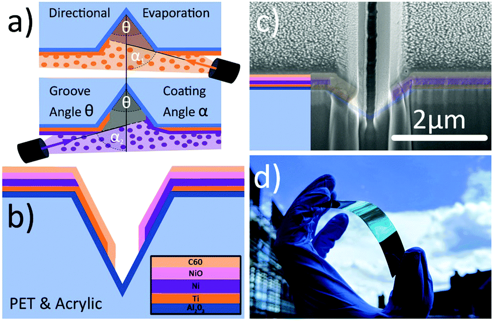 | ||
| Fig. 1 (a) Schematic illustration of directional evaporation onto a groove substrate creating selective electrodes on opposing groove walls. Consecutive layers can be deposited at different deposition angles to control the filling depth of the groove. (b) Schematic of a coated groove after a non-directional coating of Al2O3 followed by an n-type titanium & C60 electrode on one groove wall and a p-type Ni & NiO electrode on the opposite wall. (c) A focussed ion beam-scanning electron microscope image of a cross-section through a 2 μm wide single groove after the deposition of all evaporated layers. The inset and translucent shading indicates the location of the selectively deposited metal electrodes and charge-transporting layers. (d) An image of a flexible groove substrate after the deposition of all evaporated layers. | ||
Different charge-selective contact materials were coated onto opposing walls of the groove by rotating the substrates (relative to the position of the source) by 180° between deposition runs (see Fig. 1a). By adjusting the angle of incidence between coatings, it is also possible to control the relative depth over which each material was deposited into the groove. The selection of appropriate hole- and electron-transport materials (HTM) (ETM) has been critical in our development of efficient devices. Indeed, the crystallisation of the perovskite layer during deposition, perovskite defect density, surface non-radiative recombination, and the resultant Fermi level position within the bulk of the perovskite are all dependent on the choice of transport layers.19–22 For example, it has been shown that ultra-thin layers of poly(triarylamine) (PTAA) or poly(4-butylphenyldiphenylamine) (poly-TPD) can be used as HTMs to achieve remarkable VOC and fill factor (FF).22–25 Here however, our architecture requires that the charge-transport layers are easily evaporable.
As an n-type contact, we therefore utilised a multilayer-combination of C60/Ti (deposited by thermal evaporation and e-beam evaporation respectively), while the p-type contact consisted of NiO/Ni. Here, the NiO was deposited by a reactive electron-beam evaporation process, in which metallic Ni pellets were heated by an electron-beam under vacuum in a partial pressure of O2. (Note, we have measured the temperature of the PET:acrylic substrate during a typical e-beam deposition, and find that it does not exceed 100 °C.) To minimise the sheet-resistance of the device, the metal contacts deposited had a thickness of around 250 nm. We have previously demonstrated the effectiveness of reactive e-beam to deposit NiO as a p-type material in conventional planar perovskite solar cells – even without the necessity for thermal annealing.26 Notably, we have previously found that NiO films fabricated using reactive electron-beam deposition are oxygen-rich; a property previously shown to be promote efficient hole extraction in PSC devices.21
As an n-type material, we have used C60. This material was selected following a series of screening experiments, in which a series of different evaporable ETMs were investigated. Here, C60 was found to produce the most reproducible, lowest hysteresis and, highest performance conventional planar PSCs, without the need for a high-temperature anneal. The stabilised PCE output of an ITO/C60/MAPbI3/spiro-OMeTAD/Au PSC is shown in Fig. S1 (ESI†), demonstrating that thermally evaporated C60 can act as an effective electron transporting and hole blocking layer below a MAPbI3 perovskite active layer, allowing ∼14% PCE standard architecture PSCs to be created.
The flexibility of the coated, embossed substrate is clearly evident from the image shown in Fig. 1d. Here, the grooves run parallel to the long-axis of the flexible strip. To convert the surface-coated charge-selective groove structures into back-contact perovskite solar cells, flexible substrates (similar to those shown in Fig. 1d) were first cut into pieces, creating grooves whose length varied between 4 and 20 mm. These were then spin-cast at 6000 revolutions per minute (rpm) with acetonitrile-based methylammonium lead halide (MAPbI3) solution, resulting in the formation of a MAPbI3 film. Here, the perovskite material that filled the groove acted as the device active layer, with the device having the multilayer structure Ti/C60/MAPbI3/NiO/Ni. To deposit the perovskite active layer, we have used a precursor ink based on the low viscosity, low boiling point solvent acetonitrile containing MAPbI3 that had been previously bubbled using methylamine gas.27 This perovskite precursor ink combines the advantages that (i) the acetonitrile solvent does not damage the PET:acrylic substrate, and (ii) it does not require thermal annealing to generate the final perovskite. Fig. 2a shows an SEM image of a focussed-ion beam cross-section through a 2 μm wide groove filled with a MAPbI3 active layer. Interestingly, it can be seen that only very limited amounts of perovskite are found on the flat surfaces either side of the groove.
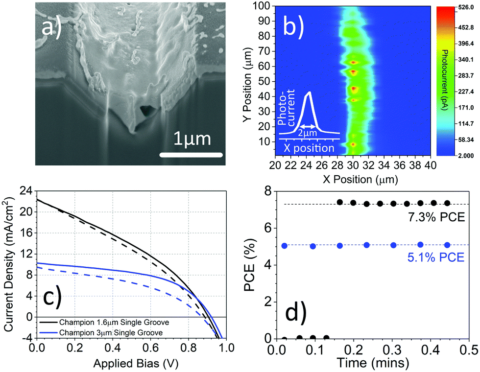 | ||
| Fig. 2 (a) A focussed ion beam-scanning electron microscope cross-section image of a 2 μm wide MAPbI3 coated groove. (b) A laser-beam-induced current map of a single MAPbI3 filled groove, inset is cross-section of the LBIC map. (c) Current–voltage curves of champion 1.6 μm (black) and 3 μm (blue) wide single grooves. Solid lines and dotted line represent reverse and forward sweeps respectively. (d) Stabilised power conversion efficiency outputs for the same champion grooves. Performance metrics of these devices are given in Table 1. | ||
Results and discussion
To confirm that the structures created act as a photovoltaic device, it was first determined that photocurrent could be generated from the perovskite material that filled the V-shaped groove. This was done by focussing a chopped 635 nm laser to a 2 μm (near diffraction-limited) spot on the substrate surface. This spot was then raster-scanned across the surface in steps of 0.5 μm while the photocurrent was recorded using a lock-in amplifier. Fig. 2b plots a typical LBIC image of a 2 μm wide device. Here it can be seen that even though the spot size is approximately coincident with the width of the groove, the majority of the photocurrent appears localised within the groove. As might be expected, the flat regions either side of the groove contribute very little photocurrent, with the peak of the photocurrent being located in the centre of the groove. It is also apparent that there are variations in local photocurrent generated along the length of the groove; a result that most likely indicates that the perovskite does not uniformly fill the groove. We can use such a measurement to make a first estimation of the total active area of each individual groove PSC device from the product of the groove width (as measured using FIB-SEM) and its length. Although this methodology is relatively crude and open to error, we later describe the use of a self-masking technique to demonstrate that such methods provide an accurate measure of the device active area.Having provided a first estimate of device active area, we now proceed to measure device efficiency. Here, current–voltage (JV) sweeps were measured for individual PSC grooves when illuminated by simulated AM1.5 radiation calibrated to 100 mW cm−2. Fig. 2c plots JV sweeps for 1.6 and 3 μm wide grooves; from this we determine that the 1.6 μm wide groove had a PCE of 7.0%, while the 3 μm wide groove had a relatively high FF of 51%. We tabulate the performance metrics and active area of the grooves in Table 1. Here the enhanced FF and significantly higher shunt resistance of the wider groove suggests a relative reduction in leakage pathways between the opposing wall contacts. Stabilized power outputs of the grooves are plotted in Fig. 2d, with the 1.6 and 3 μm wide grooves having a stabilised efficiency of 7.3% and 5.1% PCE respectively.
| Groove width (μm) | PCE [%] | J SC [mA cm−2] | V OC [V] | FF [%] | Active area [cm2] |
|---|---|---|---|---|---|
| 1.6 | 7.03 (7.3) | 22.33 | 0.91 | 34.8 | 6.4 × 10⁻⁵ |
| 3 | 4.83 (5.1) | 10.33 | 0.92 | 51.0 | 1.2 × 10⁻⁴ |
We can gain further insight into the operation of our groove devices using a simple 2D model that accounts for charge carrier generation and collection probabilities to simulate the generation of a photocurrent. This model uses the accepted values of MAPbI3 minority (hole) carrier diffusion length (Ld) and absorption coefficient (D) to determine the ideal groove width (and depth) for a symmetric groove (see further details in the ESI†). We have used this model to explore the dependence of photocurrent generation on groove width, and find that there is a trade-off between parasitic recombination and optical absorption. As is shown in Fig. S3 (ESI†), our model indicates that the ideal width of a MAPbI3 filled groove should be ∼1.1 μm; a value close to the width of the smallest grooves that can be fabricated reproducibly (1.6 μm).
We have also simulated the effect of minority carrier diffusion length on photocurrent generation and groove device PCE as shown in ESI,† Fig. S3b and S4, and find that these parameters increase with increasing values of Ld. Note however that there are significant limitations in this simulation, as it does not account for recombination effects at the grain boundaries or electrode interfaces, nor does it include the effect of ion migration and its associated effects on surface recombination. Nevertheless, this model provides a practical approach to designing groove architectures for all carrier diffusion lengths, and indicates that grooves having a width of less than 2 μm should provide optimum device performance when utilising MAPbI3 processed from acetonitrile. We note that wider grooves will also retain functionality due to photon recycling effects; a phenomenon that has been observed in metal-halide perovskite materials. Here, long-lived free charges can recombine radiatively with other free charges, with newly generated photons being re-absorbed and thus resulting in further photo-excitation. This effect has been shown to allow charge collection from MAPbI3 over length scales greater than reported charge diffusion lengths, even when electrodes are as far as 50 μm apart.28
Our simulations indicate that narrower grooves have a higher PCE. We can in fact fit the JV curves of single groove devices to a simple diode model of a solar cell (see Fig. S5, ESI†), and determine a crude estimate for the diode ideality factor of ∼5. We note that a VOC of over 0.9 V can be both obtained experimentally and through simulation grooves having a width of both 1.6 and 3 μm. We note that this value of VOC is lower than conventional planar-cell architecture PSCs utilising NiO or C60.29 Indeed, we have previously reported a VOC of 1.06 V using the same reactive electron-beam evaporated NiO in inverted PSCs.26 The high ideality factor that we determine (due to high series resistance and low shunt-resistance) and voltage loss suggest that there are additional non-radiative mechanisms present in our PSC grooves. This could be due to reduced quasi-Fermi level splitting in the perovskite, increased surface recombination at the contact material interfaces, or incomplete coverage of charge-transport materials, all of which can be improved with further optimisation of device fabrication processes. We note that PSCs commonly make use of additional interlayers (e.g. phenyl-C61-butyric acid methyl ester, bathophenanthroline, bathocuproine) alongside the C60 ETM, and can employ metal doping of nickel oxide (with cobalt, magnesium or copper) to lower the valence band energy of the resultant HTM film.30–33 We believe that further modification to the directionally evaporated electrodes may allow us to further increase the VOC of our devices.
We now discuss the construction of IBC micro-modules that are created through the serial connection of adjacent PSC grooves. Here we study structures in which 3, 4, 6 and 16 grooves were fabricated using the same embossing and directional coating techniques that were used to deposit n- and p-type contacts onto the walls of a single groove. Fig. 3a presents a schematic of a groove micro-module, illustrating that the flat sections between the grooves constitute a series connection between n- and p-type contacts on neighbouring walls, creating a PV micro-module built from multiple solar cells (here represented as simple photodiodes). Such a multi-groove micro-module will in principle allow large open-circuit voltages to be built, with the voltage ideally scaling with the number of grooves in the module. ESI,† Fig. S6 indicates that both the spacing between the grooves and the groove widths can be tuned.
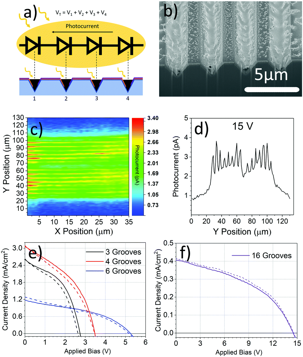 | ||
| Fig. 3 (a) Simple schematic demonstrating how multiple grooves form a micro-module. (b) A focussed ion beam-scanning electron microscopy image of a perovskite coated multi-groove. (c) Laser-beam-induced current map across 16 multi-groove micro-module, recorded at a step size of 1 μm. (d) Cross-section of the induced photocurrent map shown in part (c). (e) Current–voltage curves of champion MAPbI3 filled 3, 4 and 6 multi-groove micro-modules and, (f) current–voltage curves of a 16 groove micro-module. Solid lines and dotted line represent reverse and forward sweeps respectively. PV device performance metrics of micro-modules are shown in Table 2. | ||
Fig. 3b presents a FIB-SEM image of a multi-groove module in which it can be seen that the MAPbI3 perovskite fills each groove while leaving the flat sections between the grooves largely uncoated. Additional images of unfilled micro-module groove arrays are provided in Fig. S7 (ESI†). We have performed LBIC measurements on a micro-module composed of 16 grooves. The results of this measurement are shown in Fig. 3c, with Fig. 3d displaying a cross-section across the photocurrent map. It can be seen that 15 out of the 16 grooves are clearly resolved, with one of the 16 grooves apparently generating very little photocurrent, indicating that it is likely at short-circuit. This measurement indicates that higher efficiencies from such micro-modules can be expected following further groove embossing and device fabrication optimisation.
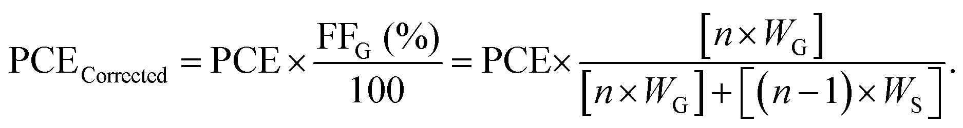
We have also tested the performance of the micro-modules by measuring their JV response under illumination with AM1.5 radiation. Since the LBIC measurements indicate that the regions between the grooves do not generate significant photocurrent, we use a geometrical fill factor to adjust module efficiency to account for the inactive regions between the grooves. Geometric fill factors (FFG) are thus calculated via a ratio of total module area to usable groove active area using eqn (1), where n is number of grooves, WG groove width, and WS is the spacing between the grooves.
 | (1) |
Fig. 3e plots champion current–voltage characteristics of micro-modules consisting of 3, 4, and 6 grooves. Our measurements indicate that the four groove micro-module has a PCE of 4.4% and a VOC of 3.5 V. The stabilised power output of this groove is shown in ESI,† Fig. S8. In Fig. 3f we present the current–voltage response of a larger 2.6% PCE micro-module consisting of 16 grooves which builds an impressive VOC of 14.6 V. This high VOC groove micro-module also has a FF of 43.5% and generates an average voltage-per-groove of 0.91 V; a value that matches the VOC of best performing single grooves. The performance metrics of all these champion multi-groove micro-modules are given in Table 2, which also lists device active areas, geometric fill factors, geometrically corrected PCEs, and the average voltage-per-groove built in each module type.
| No of grooves | PCE [%] | J SC [mA cm−2] | V OC [V] | FF [%] | Active area [cm2] | Geometric FF [%] | Corrected PCE [%] | Voltage per groove [V] |
|---|---|---|---|---|---|---|---|---|
| 3 | 3.27 | 2.61 | 2.74 | 45.7 | 2.88 × 10⁻⁴ | 82.9 | 2.71 | 0.91 |
| 4 | 4.43 | 3.05 | 3.48 | 41.7 | 3.1 × 10⁻⁴ | 72.7 | 3.22 | 0.87 |
| 6* | 2.51 | 1.18 | 5.26 | 40.6 | 2.4 × 10⁻⁴ | 44.5 | 1.12 | 0.88 |
| 16* | 2.63 | 0.42 | 14.56 | 43.5 | 9.6 × 10⁻⁴ | 41.6 | 1.09 | 0.91 |
It is apparent that the efficiency of the solar grooves is critically dependent on the value of the active area that is used in the calculation. This problem is illustrated in Fig. 4; by illuminating the top surface of a device, it is in principle possible to generate carriers in the surrounding flat region between the V-shaped grooves that are then able to diffuse to the groove active region (see Fig. 4a). Such a diffusion process will clearly result in an over-estimate of device efficiency; a problem frequently encountered when testing PSCs without an illumination mask.34 Unfortunately, the width of the individual grooves is too small to use an external illumination mask. However, the thick metal contacts on the walls can be used as an internal illumination mask provided that the device is illuminated through its substrate (see Fig. 4b). Using FIB-SEM cross-sections of a groove as shown in Fig. 4c, we can measure the width of the aperture subtended by the region at the bottom of the groove that is uncoated with a metal. Note that we have performed control UV-visible absorption measurements on (un-embossed) PET:acrylic substrates both with and without electrodes/charge-extraction contacts, and find that the optical transmission through electrode coated films is negligible (see Fig. S9, ESI†). Encouragingly, we find that the PCE of the champion 4-groove micro-module is 4% when illuminated from the front surface, and 4.4% when illuminated through the underlying substrate (see Table S1, ESI†). We note that this method indicates the PCEs reported here may even be an underestimate to the true PCE, however we cautiously interpret this as a relative error in device efficiency (determined on the basis of groove area) of 10% at most.
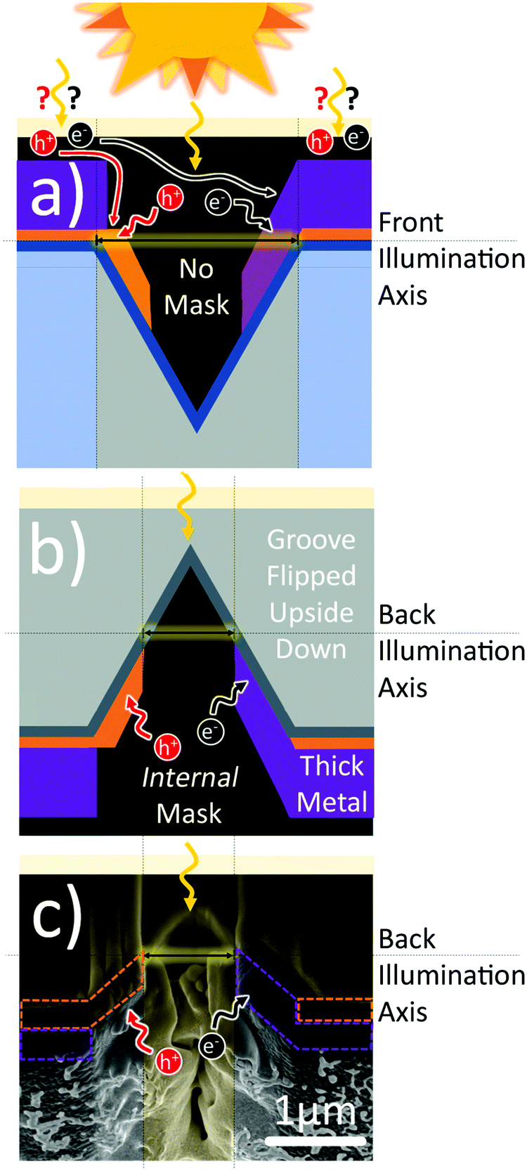 | ||
| Fig. 4 Schematic indicating two methods used to determine the active area of the grooves. Part (a) indicates the use of the physical width of the groove to calculate active area, where the width is defined by the embossing process. It is possible that photogenerated charges could be diffusing to the charge selective groove walls from outside the groove width. In part (b) the groove is illuminated through the device substrate. Here, the thick electrodes act as internal illumination mask. The width of the aperture at the bottom of the groove is determined from focussed ion beam-scanning electron microscopy images, presented in part (c), where the image of the device is orientated to show how it might look upon illumination from the back. Here, there can be no photogenerated charges diffusing from outside the defined illuminated area. | ||
We have performed some preliminary device optimisation studies focussing on understanding the effect of the spin-coating velocity used to coat the perovskite precursor ink. Here, we have explored two perovskite deposition conditions in which the perovskite solution was either spin-coated at 2000 rpm or 6000 rpm. We find that the faster spin speeds lead to the creation of semi-filled grooves with very little perovskite material found between grooves. In contrast, the slower spin speed results in the formation of a fully-filled groove, with the flat surfaces either side of the groove being coated by a layer of perovskite that is hundreds of nanometres thick. This can be seen in ESI,† Fig. S10 that compares FIB-SEM cross-sections of grooves coated with perovskite deposited using both spin speed conditions.
We have explored the statistical variation in solar groove efficiency as shown in Fig. 5. Here, we present boxplots of device performance metrics for (N = 5) single groove devices and 16-groove micro-modules when either coated by a thin (conformally semi filling the groove) or thick (fully filling the groove) MAPbI3 absorbing layer. It can be seen that there is a significant variation in performance metrics within each boxplot; a result that most likely originates from variations in the degree to which the perovskite fills each groove. It is also apparent that device efficiency is dependent on the thickness of the perovskite film. Interestingly, we find that the use of a thicker perovskite film results in single-groove devices that have slightly reduced average efficiency than comparable devices containing a thinner perovskite film, being (3.8 ± 0.5)% and (4.8 ± 0.3)% respectively. This contrasts with multi-groove modules that demonstrate a higher peak PCE of 3.8% when a thicker perovskite is used relative to 2.2% for modules incorporating a thinner perovskite. This variation in efficiency results from a loss in average VOC, with this effect apparent in both single-groove devices and multi-groove modules. However, in the case of multi-groove micro-modules, the photocurrent is apparently higher when employing thicker perovskite active layers; an effect that offsets the loss of PCE due to the lower VOC. We believe this loss in VOC results from the presence of the thick layer of perovskite between grooves that generates short circuit pathways for photogenerated charges between the different grooves. This suggests that for every groove shape, size and pattern, there is likely to be an optimum perovskite coating thickness.
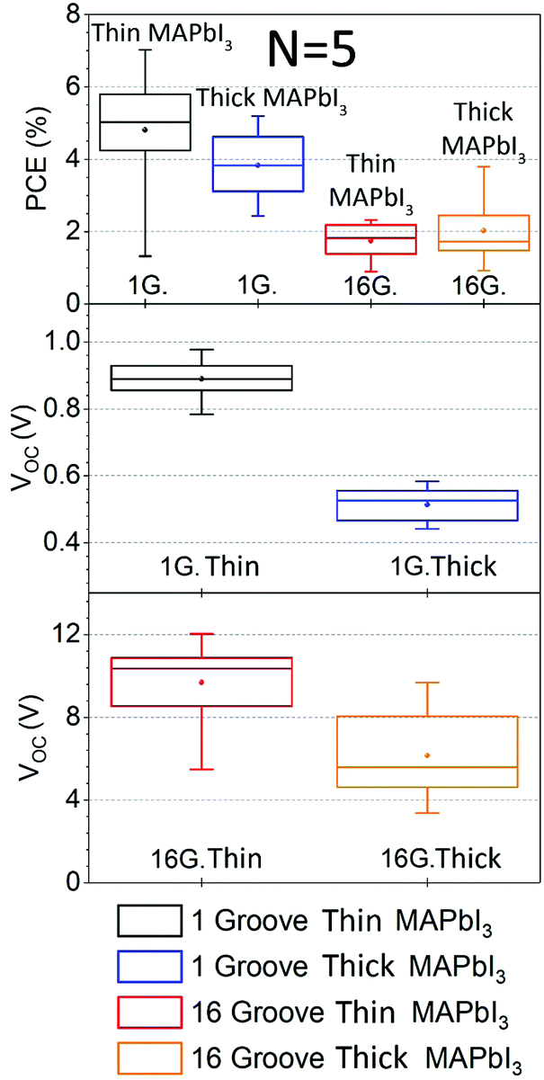 | ||
| Fig. 5 Boxplots showing distribution of power conversion efficiency and open circuit voltage for a batch of single grooves (black, blue) and 16 groove (red, orange) solar micro-modules. Here, the thickness of the perovskite in the grooves is varied through control of the MAPbI3 deposition conditions. Devices based on thick MAPbI3 shown using blue and orange lines, while the thinner MAPbI3 active later is indicated using black and red lines. | ||
Successful commercialisation of perovskite solar modules requires demonstration of efficiency, scalability, and stability. As such, it has become a recent goal of the perovskite solar scientific community to progress from focussing on one or two of these requirements to tackling all three simultaneously.35 For this reason we have started to explore the operational stability of MAPbI3 micro-groove back-contact solar modules. Indeed, we have determined the intrinsic stability of PSC grooves when stored in the dark under a N2 atmosphere for 150 days. Fig. 6 plots a JV sweep of a PSC groove before and after this storage period, with its performance metrics listed in Table 3. It can be seen that all performance metrics improve over time, including a significant increase of 0.14 V in the open circuit voltage.
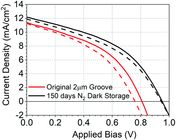 | ||
| Fig. 6 Current–voltage curves of a 2 μm wide single groove after fabrication (red) and after 150 days stored in the dark under N2 (black). Solid lines and dotted line represent reverse and forward sweeps respectively. | ||
| Time stored in dark in N2 | PCE [%] | J SC [mA cm−2] | V OC [V] | FF [%] |
|---|---|---|---|---|
| 0 days | 3.99 | 11.40 | 0.81 | 43.26 |
| 150 days | 5.04 | 12.20 | 0.95 | 43.54 |
Whist this initial result is promising, perovskite modules will ultimately need to pass the relevant International Electrotechnical Commission (IEC) stability standard (IEC 61215); here the most challenging tests include stress testing with repeated thermal cycling (−40 to 85 °C), moisture storage (80% RH), and extended damp heat storage (85 °C + 80% RH).36,37 Unfortunately, whilst MAPbI3 has proven easy to process, it is thermally unstable within the expected maximum operating conditions of a solar module.37 Indeed MAPbI3 perovskites have also been shown to be unstable due to moisture,38 and oxygen in combination with light,39 so ultimately they will require encapsulation to retard degradation. This encapsulation must minimise moisture ingress and trap any volatile components from escaping (to maximise any reversible reformation of degraded perovskite),40 without causing delamination of any of the underlying layers. Our preliminary strategy for encapsulation involves the use of 3 M barrier films (3 M UBF-512). In Fig. S11 (ESI†) we present images of MAPbI3 coated PET:acrylic substrates that were either left unencapsulated or sealed with 3 M barrier encapsulation and were stored at 80% relative humidity for 3 weeks, with Fig. S12 (ESI†) quantifying the optical absorption of the same samples. It can be seen that this preliminary encapsulation technique clearly prevents the perovskite from visibly degrading. However, at this stage we do not expect the MAPbI3 filled grooves to remain stable upon damp-heat storage or long-term thermal cycling until an alternative composition for the perovskite is utilised.
We have also performed preliminary measurements on a series of different substrates that have been subject to thermal stress before the deposition of the perovskite to characterise the sensitivity of the flexible substrate and the charge extraction materials. Here, we first compared the performance of PSC grooves that were fabricated onto a substrate (before n and p-type contact deposition) that was initially either stored at room temperature in air or placed on a substrate at 110 °C for one hour in air (see Fig. S13a, ESI†). Here, we find that the PSC grooves fabricated onto the heat treated substrate exhibited an improvement in all device metrics. This indicates that the PET:acrylic groove substrate does not appear to have any significant thermal stability issues.
We then explored the individual thermal stability of the p-type and n-type contacts. This was done by first testing the performance of devices fabricated onto PET:acrylic grooves that had been heated after all electrodes and charge-transporting materials had been deposited (see Fig. S13b, ESI†). This was compared with devices fabricated onto heat-treated grooves where all materials except the C60 had been deposited (see Fig. S13c, ESI†). Here, the remaining layers (C60 and perovskite) were then deposited after the heat treatment (110 °C for one hour in air). We tabulate the average and standard deviation performance metrics of 3 PSC grooves fabricated following each of these treatments in Table S2 (ESI†). We find that the PSC grooves in which all materials were thermally-stressed (including the C60) underwent degradation with all performance metrics dropping, leading to an overall relative reduction of 50% PCE. Conversely, the grooves that were thermally stressed before the deposition of the C60 (but with all other electrode materials in place) underwent no significant change in performance metrics. These preliminary studies indicate that the Ni/NiO interface is thermally stable, whilst the Ti/C60 interface is not.
We note that Ni/NiO/MAPbI3 and C60/MAPbI3 material stacks have previously been successfully implemented into flat-cell PSC architectures, achieving reasonable long-term stability.41,42 However, our studies indicate that a Ti/C60/MAPbI3 multilayer has reduced thermal stability. Future work will address the development of new n-type contacts, together with the utilisation of perovskite alloys containing formamidinium (FA), methylammonium and cesium cations which have been shown to produce PSCs with enhanced stability.43 We note that FA has recently been incorporated into a roll-to-roll deposition process utilising an acetonitrile-based perovskite precursor solution, which may prove suitable for coating groove-based devices.44 Our simulations also indicate that new processing routes, that lead to larger grain sizes as well as longer minority carrier diffusion lengths are expected to further improve the efficiency of micro-groove solar devices.
Conclusions
In conclusion, we have fabricated flexible MAPbI3 micro-groove back-contact solar cells reaching a PCE of 7.3%. Micro-modules are also created through the serial connection of adjacent grooves, with such modules achieving a champion PCE of 4.4%, with other modules building an open-circuit voltage of up to 14.6 V. These back-contact micro-modules are fully functional without the use of electrode patterning techniques such as electrodeposition, laser ablation, mechanical etching, or photoresist templating. The techniques we have developed do not require high temperature substrate conditioning, are free from the complex cocktail of dopants that are often used to increase the conductivity of charge-transport materials in PSCs45 and do not contain rare metals such as gold, silver or indium that are commonly used in PSCs. We outline a framework of preliminary stability measurements to demonstrate the viability of this technology for commercialization. The process techniques we have developed are conceptually similar to the low-cost metallisation of plastic used in the food packing industry,46 and thus the use of inexpensive metals, metal oxides, and flexible polymeric substrates make the technology outlined suitable for scalable, high throughput roll-to-roll processes.47,48 This unique back-contact architecture (patented by Power Roll Ltd) also presents an exciting opportunity to allow surface-sensitive in situ studies of perovskites to be made during device operation – for example – allowing the optoelectronic and crystal properties of the perovskite active layer to be investigated as it is deposited or during post-deposition treatments.Methods
Device fabrication
![[thin space (1/6-em)]](https://www.rsc.org/images/entities/char_2009.gif) :1.06 lead(II) iodide (PbI2, TCI, perovskite precursor) and methylammonium iodide (MAI, dyesol) was mixed at a ratio of 1:1.06 MAI:PbI2 to obtain a black powder suspension. As described by Noel et al.,27 the suspension was then bubbled with dry methylamine until a clear (yellow) solution was obtained. This solution was then filtered through a 0.2 μm polytetrafluoroethylene filter, with 40 μl of the resultant solution spin coated onto the groove substrates at a speed between 2000 and 6000 rpm in a N2 filled glovebox. The resultant PSC grooves were not thermally annealed.
:1.06 lead(II) iodide (PbI2, TCI, perovskite precursor) and methylammonium iodide (MAI, dyesol) was mixed at a ratio of 1:1.06 MAI:PbI2 to obtain a black powder suspension. As described by Noel et al.,27 the suspension was then bubbled with dry methylamine until a clear (yellow) solution was obtained. This solution was then filtered through a 0.2 μm polytetrafluoroethylene filter, with 40 μl of the resultant solution spin coated onto the groove substrates at a speed between 2000 and 6000 rpm in a N2 filled glovebox. The resultant PSC grooves were not thermally annealed.
Device and film characterisation
Conflicts of interest
D. G. L. and A. R. B. are co-directors of the company Ossila Ltd that retails materials used in perovskite photovoltaic research. PowerRoll Ltd hold the following patents relating to the substrates used in this work: Canada 2840327, China, 201180071841.6, 201480006419.6, Europe 2724380, EP 2951866, USA 14/264670, 14/764599, South Africa 2014/00531, Brazil BR1120150175007, Hong Kong 16103709.8, India 2812/KOLNP/2015, Japan 2015-555797, UK GB2487419.Acknowledgements
This work was partly funded by the UK Engineering and Physical Sciences Research Council (EPSRC) via grant EP/M025020/1 ‘High resolution mapping of performance and degradation mechanisms in printable photovoltaic devices’ and EP/M014797/1 ‘Improved Understanding, Development and Optimization of Perovskite-based Solar Cells’. We also thank the EPSRC for PhD studentships via the University of Sheffield DTG account (T. R. and J. B.) and from the Centre for Doctoral Training in New and Sustainable PV, EP/L01551X/1 (M. S. and J. S.). We would like to thank Budhika Mendis at Durham University for recording the FIB-SEM images. Power Roll Ltd co-sponsored this research.References
- G. W. P. Adhyaksa, E. Johlin and E. C. Garnett, Nano Lett., 2017, 17, 5206–5212 CrossRef CAS PubMed.
- A. N. Jumabekov, E. Della Gaspera, Z.-Q. Xu, A. S. R. Chesman, J. van Embden, S. A. Bonke, Q. Bao, D. Vak and U. Bach, J. Mater. Chem. C, 2016, 4, 3125–3130 RSC.
- Q. Hou, D. Bacal, A. N. Jumabekov, W. Li, Z. Wang, X. Lin, S. H. Ng, B. Tan, Q. Bao, A. S. R. Chesman, Y.-B. Cheng and U. Bach, Nano Energy, 2018, 50, 710–716 CrossRef CAS.
- Z. Hu, G. Kapil, H. Shimazaki, S. S. Pandey, T. Ma and S. Hayase, J. Phys. Chem. C, 2017, 121, 4214–4219 CrossRef CAS.
- M. Alsari, O. Bikondoa, J. Bishop, M. Abdi-Jalebi, L. Y. Ozer, M. Hampton, P. Thompson, M. T. Hörantner, S. Mahesh, C. Greenland, J. E. Macdonald, G. Palmisano, H. J. Snaith, D. G. Lidzey, S. D. Stranks, R. H. Friend and S. Lilliu, Energy Environ. Sci., 2018, 18–20 Search PubMed.
- S. Weber, I. M. Hermes, S. H. Turren Cruz, C. Gort, V. W. Bergmann, L. Gilson, A. Hagfeldt, M. Grätzel, W. Tress and R. Berger, Energy Environ. Sci., 2018, 11, 2404–2413 RSC.
- H. J. Snaith, Nat. Mater., 2018, 17, 372–376 CrossRef CAS PubMed.
- M. A. Green and A. Ho-Baillie, ACS Energy Lett., 2017, 2, 822–830 CrossRef CAS.
- M. Yang, D. H. Kim, T. R. Klein, Z. Li, M. O. Reese, B. J. Tremolet De Villers, J. J. Berry, M. F. A. M. Van Hest and K. Zhu, ACS Energy Lett., 2018, 3, 322–328 CrossRef CAS.
- A. L. Palma, F. Matteocci, A. Agresti, S. Pescetelli, E. Calabrò, L. Vesce, S. Christiansen, M. Schmidt and A. Di Carlo, IEEE J. Photovolt., 2017, 7, 1674–1680 Search PubMed.
- J. Dagar, S. Castro-Hermosa, M. Gasbarri, A. L. Palma, L. Cina, F. Matteocci, E. Calabrò, A. Di Carlo and T. M. Brown, Nano Res., 2018, 11, 2669–2681 CrossRef CAS.
- A. Di Carlo, F. Matteocci, S. Razza, M. Mincuzzi, F. Di Giacomo, S. Casaluci, D. Gentilini, T. M. Brown, a. Reale, F. Brunetti, a. D’Epifanio and S. Licoccia, 14th IEEE Int. Conf. Nanotechnol., 2014, pp. 70–74 Search PubMed.
- S. Razza, F. Di Giacomo, F. Matteocci, L. Cinà, A. L. Palma, S. Casaluci, P. Cameron, A. D’Epifanio, S. Licoccia, A. Reale, T. M. Brown and A. Di Carlo, J. Power Sources, 2015, 277, 286–291 CrossRef CAS.
- H. C. Liao, P. Guo, C. P. Hsu, M. Lin, B. Wang, L. Zeng, W. Huang, C. M. M. Soe, W. F. Su, M. J. Bedzyk, M. R. Wasielewski, A. Facchetti, R. P. H. Chang, M. G. Kanatzidis and T. J. Marks, Adv. Energy Mater., 2017, 7, 1–9 Search PubMed.
- L. Cai, L. Liang, J. Wu, B. Ding, L. Gao and B. Fan, J. Semicond., 2017, 38, 014006 CrossRef.
- T. Ma, Q. Song, D. Tadaki, M. Niwano and A. Hirano-Iwata, ACS Appl. Energy Mater., 2018, 1(3), 970–975 CrossRef CAS.
- G. DeLuca, A. N. Jumabekov, Y. Hu, A. N. Simonov, J. Lu, B. Tan, G. W. P. Adhyaksa, E. C. Garnett, E. Reichmanis, A. S. R. Chesman and U. Bach, ACS Appl. Energy Mater., 2018, 1(9), 4473–4478 CrossRef CAS.
- D. R. Pernik, M. Gutierrez, C. Thomas, V. R. Voggu, Y. Yu, J. van Embden, A. J. Topping, J. J. Jasieniak, D. A. Vanden Bout, R. Lewandowski and B. A. Korgel, ACS Energy Lett., 2016, 1, 1021–1027 CrossRef CAS.
- P. Schulz, E. Edri, S. Kirmayer, G. Hodes, D. Cahen and A. Kahn, Energy Environ. Sci., 2014, 7, 1377–1381 RSC.
- P. Schulz, ACS Energy Lett., 2018, 3, 1287–1293 CrossRef CAS.
- P. Schulz, L. L. Whittaker-Brooks, B. A. Macleod, D. C. Olson, Y. L. Loo and A. Kahn, Adv. Mater. Interfaces, 2015, 2(7), 1400532 CrossRef.
- M. Stolterfoht, C. M. Wolff, J. A. Márquez, S. Zhang, C. J. Hages, D. Rothhardt, S. Albrecht, P. L. Burn, P. Meredith, T. Unold and D. Neher, Nat. Energy, 2018, 3, 847–854 CrossRef CAS.
- Z. Liu, L. Krückemeier, B. Krogmeier, B. Klingebiel, J. A. Márquez, S. Levcenko, S. Öz, S. Mathur, U. Rau, T. Unold and T. Kirchartz, ACS Energy Lett., 2019, 4, 110–117 CrossRef CAS.
- M. Wong-Stringer, O. S. Game, J. A. Smith, T. J. Routledge, B. A. Alqurashy, G. Benjamin, A. J. Parnell, N. Vaenas, V. Kumar, M. O. A. Alawad, A. Iraqi, C. Rodenburg and D. G. Lidzey, Adv. Energy Mater., 2018, 8, 1801234 CrossRef.
- M. Stolterfoht, C. M. Wolff, Y. Amir, A. Paulke, L. Perdigón-Toro, P. Caprioglio and D. Neher, Energy Environ. Sci., 2017, 10, 1530–1539 RSC.
- T. J. Routledge, M. Wong-Stringer, O. S. Game, J. A. Smith, J. E. Bishop, N. Vaenas, B. G. Freestone, D. M. Coles, T. McArdle, A. R. Buckley and D. G. Lidzey, J. Mater. Chem. A, 2019, 7, 2283–2290 RSC.
- N. K. Noel, S. N. Habisreutinger, B. Wenger, M. T. Klug, M. T. Hörantner, M. B. Johnston, R. J. Nicholas, D. T. Moore and H. Snaith, Energy Environ. Sci., 2016, 10, 145–152 RSC.
- L. M. Pazos-Outón, M. Szumilo, R. Lamboll, J. M. Richter, M. Crespo-Quesada, M. Abdi-Jalebi, H. J. Beeson, M. Vrućinić, M. Alsari, H. J. Snaith, B. Ehrler, R. H. Friend and F. Deschler, Science, 2016, 351, 1430–1433 CrossRef PubMed.
- S. Sajid, A. M. Elseman, H. Huang, J. Ji, S. Dou, H. Jiang, X. Liu, D. Wei, P. Cui and M. Li, Nano Energy, 2018, 51, 408–424 CrossRef CAS.
- K. Yao, F. Li, Q. He, X. Wang, Y. Jiang, H. Huang and A. K. Y. Jen, Nano Energy, 2017, 40, 155–162 CrossRef CAS.
- S. Hong, J. Lee, H. Kang, G. Kim, S. Kee, J.-H. Lee, S. Jung, B. Park, S. Kim, H. Back, K. Yu and K. Lee, Sci. Adv., 2018, 4, eaat3604 CrossRef PubMed.
- G. Li, Y. Jiang, S. Deng, A. Tam, P. Xu, M. Wong and H. S. Kwok, Adv. Sci., 2017, 4, 1–8 Search PubMed.
- Y. Xie, K. Lu, J. Duan, Y. Jiang, L. Hu, T. Liu, Y. Zhou and B. Hu, ACS Appl. Mater. Interfaces, 2018, 10, 14153–14159 CrossRef CAS PubMed.
- J. A. Christians, J. S. Manser and P. V. Kamat, J. Phys. Chem. Lett., 2015, 6, 852–857 CrossRef CAS.
- J. A. Christians, F. Zhang, R. C. Bramante, M. O. Reese, T. H. Schloemer, A. Sellinger, M. F. A. M. Van Hest, K. Zhu, J. J. Berry and J. M. Luther, ACS Energy Lett., 2018, 3, 2502–2503 CrossRef CAS.
- L. Shi, T. L. Young, J. Kim, Y. Sheng, L. Wang, Y. Chen, Z. Feng, M. J. Keevers, X. Hao, P. J. Verlinden, M. A. Green and A. W. Y. Ho-Baillie, ACS Appl. Mater. Interfaces, 2017, 9, 25073–25081 CrossRef CAS PubMed.
- P. Holzhey and M. Saliba, J. Mater. Chem. A, 2018, 6, 21794–21808 RSC.
- A. M. A. Leguy, Y. Hu, M. Campoy-Quiles, M. I. Alonso, O. J. Weber, P. Azarhoosh, M. Van Schilfgaarde, M. T. Weller, T. Bein, J. Nelson, P. Docampo and P. R. F. Barnes, Chem. Mater., 2015, 27, 3397–3407 CrossRef CAS.
- Q. Sun, P. Fassl, D. Becker-Koch, A. Bausch, B. Rivkin, S. Bai, P. E. Hopkinson, H. J. Snaith and Y. Vaynzof, Adv. Energy Mater., 2017, 7(20), 1700977 CrossRef.
- E. J. Juarez-Perez, L. K. Ono, M. Maeda, Y. Jiang, Z. Hawash and Y. Qi, J. Mater. Chem. A, 2018, 6, 9604–9612 RSC.
- B. Abdollahi Nejand, V. Ahmadi and H. R. Shahverdi, ACS Appl. Mater. Interfaces, 2015, 7, 21807–21818 CrossRef CAS PubMed.
- H. Zhang, J. Cheng, F. Lin, H. He, J. Mao, K. S. Wong, A. K. Y. Jen and W. C. H. Choy, ACS Nano, 2016, 10, 1503–1511 CrossRef CAS.
- M. Saliba, T. Matsui, J.-Y. Seo, K. Domanski, J.-P. Correa-Baena, M. K. Mohammad, S. M. Zakeeruddin, W. Tress, A. Abate, A. Hagfeldt and M. Gratzel, Energy Environ. Sci., 2016, 9, 1989–1997 RSC.
- B. Dou, J. B. Whitaker, K. Bruening, D. T. Moore, L. M. Wheeler, J. Ryter, N. J. Breslin, J. J. Berry, S. M. Garner, F. S. Barnes, S. E. Shaheen, C. J. Tassone, K. Zhu and M. F. A. M. van Hest, ACS Energy Lett., 2018, 3(10), 2558–2565 CrossRef CAS.
- M. Wong-Stringer, J. E. Bishop, J. A. Smith, D. K. Mohamad, A. J. Parnell, V. Kumar, C. Rodenburg and D. G. Lidzey, J. Mater. Chem. A, 2017, 5, 15714–15723 RSC.
- G. A. Abbas, Z. Ding, H. E. Assender, J. J. Morrison, S. G. Yeates, E. R. Patchett and D. M. Taylor, Org. Electron. Phys., Mater. Appl., 2014, 15, 1998–2006 CAS.
- Z. Song, C. L. McElvany, A. B. Phillips, I. Celik, P. W. Krantz, S. C. Watthage, G. K. Liyanage, D. Apul and M. J. Heben, Energy Environ. Sci., 2017, 10, 1297–1305 RSC.
- J. Gong, S. B. Darling and F. You, Energy Environ. Sci., 2015, 8, 1953–1968 RSC.
Footnotes |
| † Electronic supplementary information (ESI) available. See DOI: 10.1039/c8ee03517b |
| ‡ These authors contributed equally to this work. |
| This journal is © The Royal Society of Chemistry 2019 |