
 Open Access Article
 This Open Access Article is licensed under a
 Creative Commons Attribution 3.0 Unported Licence
Lattice strain causes non-radiative losses in halide perovskites†
Timothy W.
Jones‡
 a,
Anna
Osherov‡
b,
Mejd
Alsari‡
c,
Melany
Sponseller
b,
Benjamin C.
Duck
a,
Young-Kwang
Jung
d,
Charles
Settens
b,
Farnaz
Niroui
b,
Roberto
Brenes
b,
Camelia V.
Stan
e,
Yao
Li
ef,
Mojtaba
Abdi-Jalebi
c,
Nobumichi
Tamura
e,
J. Emyr
Macdonald
g,
Manfred
Burghammer
h,
Richard H.
Friend
c,
Vladimir
Bulović
b,
Aron
Walsh
di,
Gregory J.
Wilson
a,
Samuele
Lilliu
j and
Samuel D.
Stranks
*bc
a,
Anna
Osherov‡
b,
Mejd
Alsari‡
c,
Melany
Sponseller
b,
Benjamin C.
Duck
a,
Young-Kwang
Jung
d,
Charles
Settens
b,
Farnaz
Niroui
b,
Roberto
Brenes
b,
Camelia V.
Stan
e,
Yao
Li
ef,
Mojtaba
Abdi-Jalebi
c,
Nobumichi
Tamura
e,
J. Emyr
Macdonald
g,
Manfred
Burghammer
h,
Richard H.
Friend
c,
Vladimir
Bulović
b,
Aron
Walsh
di,
Gregory J.
Wilson
a,
Samuele
Lilliu
j and
Samuel D.
Stranks
*bc
aCSIRO Energy Centre, Mayfield West, NSW 2304, Australia
bResearch Laboratory of Electronics, Massachusetts Institute of Technology, 77 Massachusetts Avenue, Cambridge, Massachusetts 02139, USA. E-mail: sds65@cam.ac.uk
cCavendish Laboratory, University of Cambridge, JJ Thompson Avenue, Cambridge CB3 0HE, UK
dDepartment of Materials Science and Engineering, Yonsei University, Seoul 03722, Korea
eAdvanced Light Source, Lawrence Berkeley National Laboratory, Berkeley, California 94720, USA
fXi’an Jiaotong University, State Key Laboratory for Mechanical Behavior of Materials, Xi’an, China
gSchool of Physics and Astronomy, Cardiff University, Cardiff CF24 3AA, UK
hEuropean Synchrotron Radiation Facility, Grenoble, France
iDepartment of Materials, Imperial College London, Exhibition Road, London SW7 2AZ, UK
jDepartment of Physics and Astronomy, University of Sheffield, Sheffield S3 7RH, UK
First published on 15th January 2019
Abstract
Halide perovskites are promising semiconductors for inexpensive, high-performance optoelectronics. Despite a remarkable defect tolerance compared to conventional semiconductors, perovskite thin films still show substantial microscale heterogeneity in key properties such as luminescence efficiency and device performance. However, the origin of the variations remains a topic of debate, and a precise understanding is critical to the rational design of defect management strategies. Through a multi-scale investigation – combining correlative synchrotron scanning X-ray diffraction and time-resolved photoluminescence measurements on the same scan area – we reveal that lattice strain is directly associated with enhanced defect concentrations and non-radiative recombination. The strain patterns have a complex heterogeneity across multiple length scales. We propose that strain arises during the film growth and crystallization and provides a driving force for defect formation. Our work sheds new light on the presence and influence of structural defects in halide perovskites, revealing new pathways to manage defects and eliminate losses.
Broader contextMetal halide perovskites are generating enormous excitement for optoelectronic devices including solar cells and light-emitting diodes. However, there are still substantial numbers of defects that trap energized charge carriers, leading to power losses in devices. The origin of these defects, particularly on the micro-scale, remains unknown. In this work, the authors show that these defects are related to complicated strain patterns that appear on multiple length scales in perovskite films – ranging from tens of micrometres down to the tens of nanometre scale. The results suggest that these strain patterns are built into the film upon formation. This work has profound implications on our understanding of the operation of the materials on the micro-scale. It also highlights the need to control strain as a lever to eliminate these problematic defects in order to ultimately attain maximum device performances. |
Halide perovskite semiconductors have captured the imagination of the research community because of the unprecedented progress in performance of photovoltaic (PV) and light-emission devices, coupled with remarkably simple techniques for deposition and fabrication.1 In just six years, PV power conversion efficiencies (PCEs) have been lifted beyond 23%, along with reports of promising performances of perovskite light-emitting diodes (LEDs).2,3 However, an essential condition for PV and LED devices to reach their efficiency limits is a high luminescence efficiency in which non-radiative losses are eliminated.4 Non-radiative recombination, for example recombination of electrons and holes mediated by defect traps in the bulk or at device interfaces, is a parasitic loss pathway that limits the open-circuit voltage in solar cells. The photoluminescence (PL) quantum efficiency (PLQE) of neat perovskite films under solar illumination conditions is low (typically <10%);5 passivation post-treatments can substantially increase these values but are yet to entirely remove non-radiative losses especially in the presence of device electrodes.6–9 The important metric of external radiative efficiency for high-performance perovskite PV devices still remains ∼1%,10,11 far behind the ∼30% achieved by state-of-the-art GaAs cells.12
Macroscopic observations of non-radiative losses in perovskite films are manifested as an emission heterogeneity on the microscale, where the PL lifetime and intensity have been shown to vary between different grains even in the highest-performing polycrystalline films.13 This microscale spatial heterogeneity has also been observed in charge carrier diffusion lengths14 and in the photocurrent and open-circuit voltage in full solar cell devices.15 Together, these measurements demonstrate the impact of the microscale on the resulting macroscopic polycrystalline film properties, suggesting that there is enormous scope for improving device PCE by understanding and then addressing these heterogeneous optoelectronic properties. The literature consensus attributes non-radiative losses to a spatially-heterogeneous population of sub-bandgap electronic states that act as trap-mediated recombination sites.13,16 However, the origin of these traps and their heterogeneity is still unresolved.
Structural defects have a strong influence on the charge-carrier lifetime and recombination in semiconductors and, typically, charged point defects make efficient non-radiative recombination centers.17 Most semiconductors are intolerant to the presence of defects, with typical defect densities in crystalline silicon devices required to be no larger than ∼108–1010 cm−3.18 In contrast, trap densities in polycrystalline perovskite films in high-performing devices have been determined to be relatively large (∼1013–1018 cm−3).16,19,20 This in fact suggests a remarkable defect tolerance in perovskite films that needs to be understood in the context of the nature of the trap states and any residual non-radiative losses. Grain boundaries are a likely locus for defects sites, and large grain sizes, as viewed from scanning electron microscope (SEM) images, are implicitly preferred. Furthermore, polycrystalline perovskite films have been reported to show some degree of strain, which directly influences the macroscopic optoelectronic properties and stability,21–23 though it is unclear how the strain varies on the microscale, affects local recombination or the mechanism of the strain-related effects. Here, we directly probe the heterogeneity of high-quality perovskite thin films across multiple length scales to reveal local strain-related structural defects and their direct impact on optoelectronic behaviour.
Results
Polycrystalline methylammonium lead iodide (MAPbI3) films were solution-processed on glass cover slips or silicon substrates from lead acetate and MAI-based precursor solutions containing hypophosphorous acid additives24 (see Methods). An SEM image of the film is shown in the inset of Fig. 1a, revealing grain sizes of ∼0.5–1 μm, along with an example of the uniquely-shaped Au particles solution-processed on the film surface to allow registering and correlating the same scan area between different experiments in this work. The films have a strong preferential orientation with the 〈110〉 and 〈220〉 planes as the primary observed reflections (see Fig. S1 in the ESI,† for the full macroscopic X-ray diffraction (XRD) pattern). To characterize the local perovskite structural properties on the microscale, we utilized the scanning micro-XRD (μXRD) beamline 12.3.2 at the Advanced Light Source (ALS) with a spatial resolution on our samples of ∼2.5 μm (see Methods for further details). We held the samples under flowing nitrogen at 240 K during the measurements, which we found minimized any potential moisture degradation or beam damage.25 The summed 2D powder pattern for a 70 × 70 μm2 region indexes correctly to the tetragonal phase of MAPbI3 and the chi-integrated diffractogram from the entire region matches the macroscopic diffractogram (Fig. 1a). The 〈220〉 and 〈222〉 are the dominant reflections in the μXRD patterns due to the geometry of the experimental setup, which did not allow us to observe reflections below scattering vector q = 1.33 Å−1 (Fig. S2 and Video S1, ESI†). Line profiles show excellent match to tetragonal MAPbI326 and negligible traces of crystalline impurity peaks, consistent with minimal beam damage to the sample (see Fig. S3, ESI†).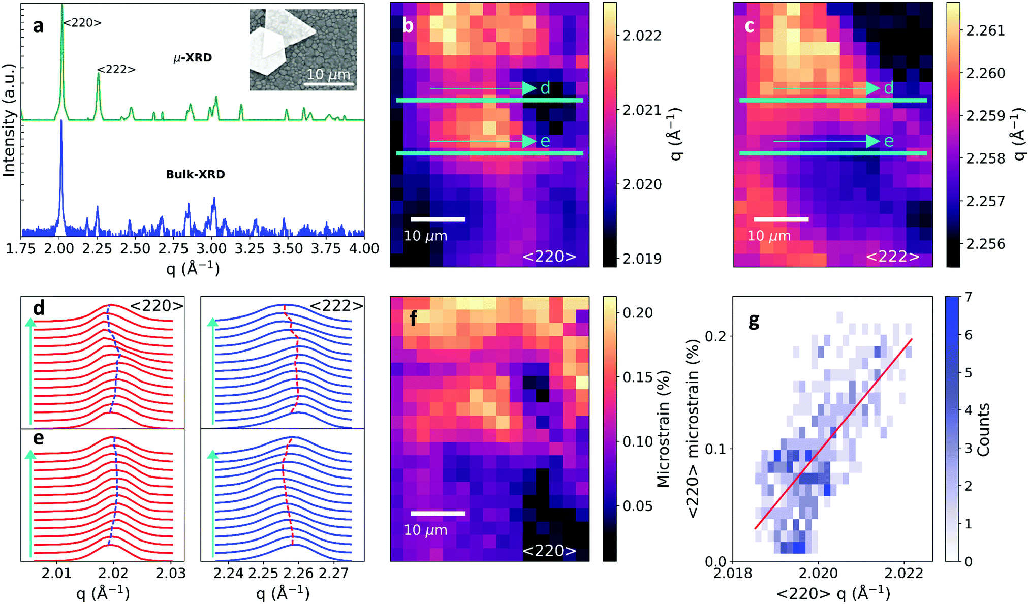 | ||
| Fig. 1 Characterising structural heterogeneity in MAPbI3 films on glass cover slips by μXRD. (a) Comparison of the macroscopic bulk XRD pattern with the μXRD pattern (both collected at 240 K) summed over a 70 × 70 μm2 spatial region, with the key reflections labelled. Inset: SEM image of the perovskite grains along with ∼ten-micrometer-sized Au fiducial marker particles. (b) Local 〈220〉 and (c) 〈222〉 diffraction peak q maps revealing substantial structural heterogeneity. (d and e) Selected slices of the 〈220〉 (red) and 〈222〉 (blue) through the maps in (b and c) illustrating the complex strain patterns present within the film. Vertical lines indicate peak position as determined through peak profile fitting and are a guide to the eye. (f) Microstrain map for the 〈220〉 diffraction peak. (g) Histogram of the calculated microstrain and corresponding scattering vector q for the 〈220〉 diffraction peak. The solid line is a linear regression fit to a scatter plot of the data, revealing a statistically-significant correlation (negligible p-value; see Methods). | ||
In Fig. 1b and c we show the spatial maps of the peak scattering vector q of the azimuthally-integrated 〈222〉 and 〈220〉 peaks (see Fig. S4 for maps of peak intensities, ESI†). These maps reveal local structural heterogeneity on the scale of beam resolution. Fig. 1d and e show the μXRD patterns taken from horizontal slices as indicated by the coloured lines on Fig. 1b and c. Subtle shifts in the peak position and broadening reveal the presence of detailed microscale structural heterogeneity. This heterogeneity in the local q vector for the 〈220〉 orientation of ∼0.15%, corresponding to a spontaneous stress of ∼19 MPa (based on a Young's modulus of 12.8 GPa27), is typical of different regions of the films measured, and is a level of heterogeneity unobservable with laboratory diffraction techniques in both spatial resolution and peak variation. Interestingly, the μXRD slice in Fig. 1d depicts a region with long-range parallel coupling between the two reflections in local q variation, whereas Fig. 1e depicts a region with anti-parallel coupling between the two reflections (Fig. S5, ESI†). These observations are evidence for complex local strain variations,21 and long-range (>10 μm) strain patterns present throughout the polycrystalline film from regions that share similar crystallographic properties, as will be discussed further below.
After subtracting the instrumental contribution towards peak broadening of the line profiles, we consider the extreme cases of contributions from microstrain-only and crystallite-size only, as defined by the Williamson–Hall formalism.28 The variance of the crystallite-size-only is considerably larger and thus we conclude that microstrain is the dominant contributor towards peak breadth in these samples (see Fig. S6 and for further discussion, ESI†). We show the resulting microstrain map of the dominant 〈220〉 reflection in Fig. 1f (see Fig. S7 for 〈222〉, ESI†). This reveals that the microstrain also has a complex local heterogeneity with a typical magnitude of ∼0.1–0.2%, indicating that each microscale region has its own local strain environment. Importantly, there is a strong correlation between q and microstrain for the 〈220〉 peak (Fig. 1g; Fig. S7 for the 〈222〉, ESI†). That is, XRD peaks with the larger local q (lower d-spacing) contain the largest structural broadening due to microstrain (and vice versa). This suggests that the strain in the polycrystalline films is compressive, i.e. acting to reduce the volume of the unit cell. We observe similar correlations in an alloyed ‘triple cation’ MA0.15FA0.79Cs0.06Pb(I0.85Br0.15)3 sample (FA = formamidinium), suggesting this observation can be generalised to other compositions29 (Fig. S8, ESI†).
To directly assess the impact of the observed strain-related defects on the perovskite optoelectronic properties, we now correlate confocal PL measurements with μXRD measurements on the same scan area. For direct comparison of the two measurements, we use the Au fiducial markers (Fig. 1a inset) and an image analysis algorithm for image registration, while also accounting for the spatial resolution differences between the measurements (see ESI† and Fig. S9–S12 for details). We show a spatial map of the local compressive strain of a region of the film in Fig. 2a. Here, we determined the local compressive strain from μXRD using the relative shift of the peak q-value at each local point from the minimum q in the distribution (i.e. strain = (qmin − q)/qmin). We show in Fig. 2b a confocal PL intensity map of the correlation region highlighted in the strain map in Fig. 2a. We note that here we are at sufficiently low excitation fluence that the local PL distribution is dominated by trap states rather than diffusion of carriers out of the local region.30 We show the local time-resolved PL measurements of a bright region and a dim region in Fig. 2c representing the recombination of charge carriers. The bright regions have a longer PL lifetime than the dark regions, which is consistent with increased fractions of trap-limited recombination in the latter. We extract trap densities representative of the regions by fitting the decays with a kinetic model developed previously,16 quantifying the reduction in trap density from the dark (7.5 × 1016 cm−3) to the bright (1 × 1016 cm−3) regions. These dark PL (trap) regions are the cause of significant power losses in solar cells, with devices fabricated from these MAPbI3 films typically showing open-circuit voltages of ∼1.1 V,8 which is ∼0.2 V from the radiative limits.
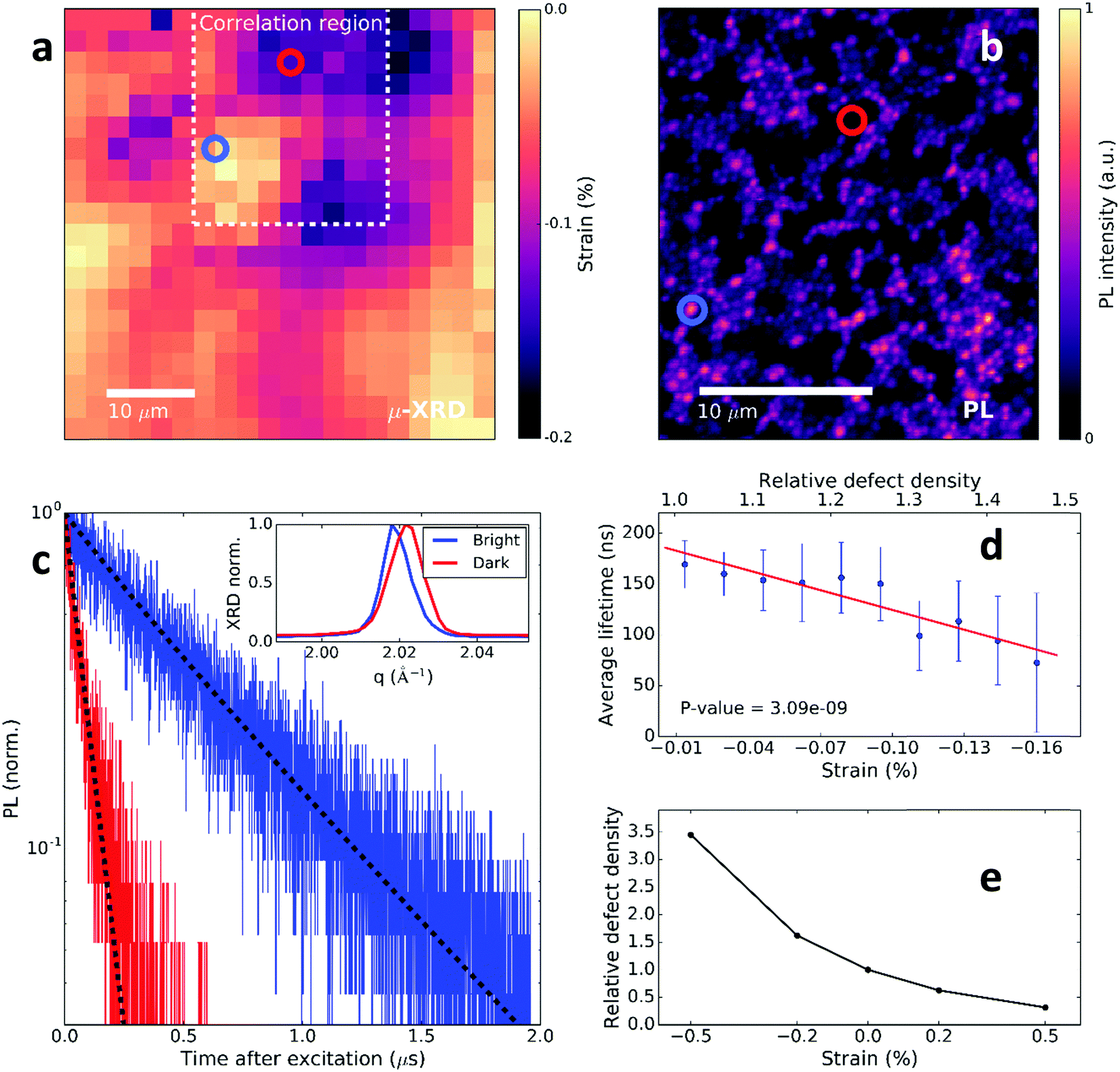 | ||
| Fig. 2 Correlating the local structural and time-resolved luminescence properties of MAPbI3 films. (a) Spatial map of the (compressive) strain variation using the relative shift of the peak q-value at each local point from the minimum q in a μXRD map (i.e. strain = (qmin − q)/qmin). The dashed line denotes the correlation region between μXRD and PL. (b) Confocal PL intensity map of a MAPbI3 perovskite film with pulsed 405 nm excitation (0.5 MHz repetition rate, 0.1 μJ per cm2 per pulse) corresponding to the dashed region in a. (c) Time-resolved PL decays of the bright (blue) and dark (red) regions highlighted in (b). The dotted lines are fits to the data using a trap model to extract the electronic trap density.16 Inset: Highlighted 〈220〉 peak diffraction pattern for the bright and dark PL regions. (d) Scatter plots of statistically-significant correlations between local PL lifetime and compressive strain (relative defect density; calculated from relationship in e). See Fig. S13 (ESI†) for other example PL decays. (e) Ratio in concentration of charged iodide vacancies (V+I defects) in 〈110〉 strained perovskite crystals to an unstrained crystal. | ||
We show in the inset of Fig. 2c the 〈220〉 μXRD peaks corresponding to the region with bright emission (long PL lifetime) and the region with dark emission (short PL lifetime). We find that the region with inferior emission intensity and carrier lifetime dynamics corresponds to a region with compressive-strained 〈220〉 lattice planes (i.e. larger q and increased peak broadening), whereas the region showing brighter emission and longer carrier lifetime is comparatively unstrained (i.e. smaller q and peak widths close to the instrumental broadening). We show in Fig. 2d that these trends appear consistently across the correlated mapped regions: scatter plots of the relevant quantities reveal a statistically-significant decrease in PL lifetime with compressive strain (see Fig. S14 for microstrain, ESI†).
Structural defects have a strong influence on the charge-carrier lifetime and recombination in semiconductors and charged point defects typically make efficient non-radiative recombination centers due to a long-range Coulomb attraction.17 We now explore the impact of a strained crystal on local point defect concentrations. Using a first-principles atomic model, we introduce compressive 〈110〉 strain with magnitude on the order observed in our local measurements (∼0.2%) and probe the effect on the point defect thermodynamics (Fig. 2e). With compressive strain, there is an increase in the charged iodide vacancy (V+I) concentration by a factor of 2 with respect to the unstrained crystal due to a negative defect pressure (see Methods and Fig. S15 and S16, ESI†). Similar behaviour is expected for other negative-pressure (strain releasing) defect species or clusters. This relative increase in defect density for a dark region ascertained from the trap model (Fig. 2c) is consistent with the calculated magnitude of the increase in strain-related halide vacancy concentrations after considering contributions from each direction (Fig. 2e). Using the relationship in Fig. 2e to convert the strain map to a relative defect density map (Fig. S17, ESI†), we show a strong anti-correlation between the PL lifetime and defect (halide vacancy) concentration ratio in Fig. 2d. These results reveal that the observation of local PL heterogeneity is substantially influenced by locally-heterogeneous strain distributions that are associated with defects such as halide vacancies. We note that we do not identify the isolated iodine vacancy as the origin of non-radiative recombination, and indeed other point and extended defects will be generated due to strain and likely also contribute to trap-assisted recombination.31–33
In order to further investigate the long range strain behaviour and its relationship to local grains, we performed scanning nanofocus XRD (nXRD) measurements at the ID13 beamline at the European Synchrotron Radiation Facility (ESRF) (Fig. S18, ESI†).26 A MAPbI3 perovskite film prepared as above was raster scanned (beam spot size 200 × 200 nm2; see Methods for details). We show a quiver plot for the 〈110〉 orientation in Fig. 3a, where the value of the azimuthal angle coordinate χp for each diffraction spot is represented using an arrow with its centre located in the spatial position from which the diffraction spot was acquired, and with an orientation and colour corresponding to χp indicated by the colour map.26 Diffraction spots adjacent both in real and reciprocal space coordinates were considered as belonging to the same cluster, here indicated as ‘super-grain’ (see Methods for details). We highlight in blue and red two super-grains with the largest covered areas calculated as the number of pixels within the super-grain times the pixel area (400 × 400 nm2). This observation of long-range features is consistent with our μXRD results, but here we visualise them with better spatial resolution. Furthermore, the super-grains also exhibit local strain (q) variations within their dimensions (Fig. 3b and c).
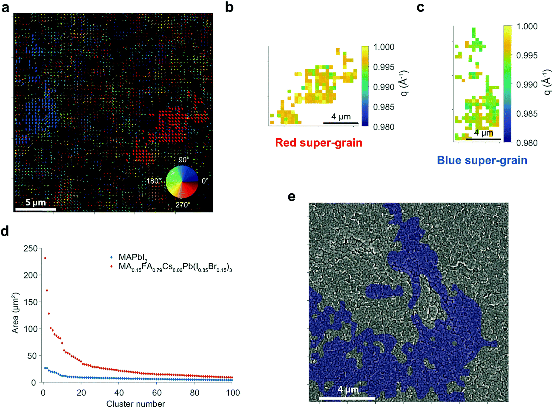 | ||
| Fig. 3 Nano-XRD measurements and super-grain analysis. (a) Quiver plot highlighting the two largest super-grains showing the 〈110〉 reflection in a MAPbI3 sample deposited on a Si/SiO2 substrate. (b and c) Local variations of the scattering vector q extracted from the two super-grains in (a). (d) Super-grain size distributions for MAPbI3 and MA0.15FA0.79Cs0.06Pb(I0.85Br0.15)3. (e) Overlay between the quiver plot (〈210〉) and SEM image in the same scan area for a MA0.15FA0.79Cs0.06Pb(I0.85Br0.15)3 sample. | ||
The super-grain sizes for the 〈110〉 reflection are plotted in Fig. 3d, showing that the largest regions cover an area of ∼25 μm2, extending well beyond the grain size observed in SEM images (∼1 μm2). We find this disparity is further exaggerated in the triple cation MA0.15FA0.79Cs0.06Pb(I0.85Br0.15)3 samples, which show super-grains as large as ∼250 μm2 (Fig. 3d) despite SEM grain sizes of only ∼0.1 μm2; this is clearly seen in the overlay of an SEM image and a quiver plot highlighting the largest super-grain in Fig. 3e (see Fig. S19 for other super-grains, ESI†). This finding could shed light onto the apparent paradox whereby ‘small-grain’ triple cation perovskite films still attain much higher PCE than these MAPbI3 films.11 Our results suggest that the critical grain size may actually be the longer-range structural super-grains rather than the grains viewed in SEM images.
To now explore crystallinity at a sub-grain resolution we turn to transmission electron microscopy (TEM). In Fig. 4a, we show a cross-sectional bright-field TEM image of the perovskite film. The sample was prepared by thinning down the 0.4 μm long lamella that appeared as an individual grain in the top-view SEM image by focused-ion beam (FIB). A selected-area electron diffraction (SAED) pattern obtained from a 200 nm region within the lamella is outlined by a circle in the micrograph and shown in the inset of Fig. 4a. The SAED pattern indicates a non-single crystalline nature of the “single grain” observed in SEM. Although the d-spacing corresponds to the tetragonal MAPbI3 perovskite structure, the presence of elongated diffraction spots as well as a weak diffraction ring is a strong indicator of imperfections within the lattice that likely originate from strain and/or other defects.
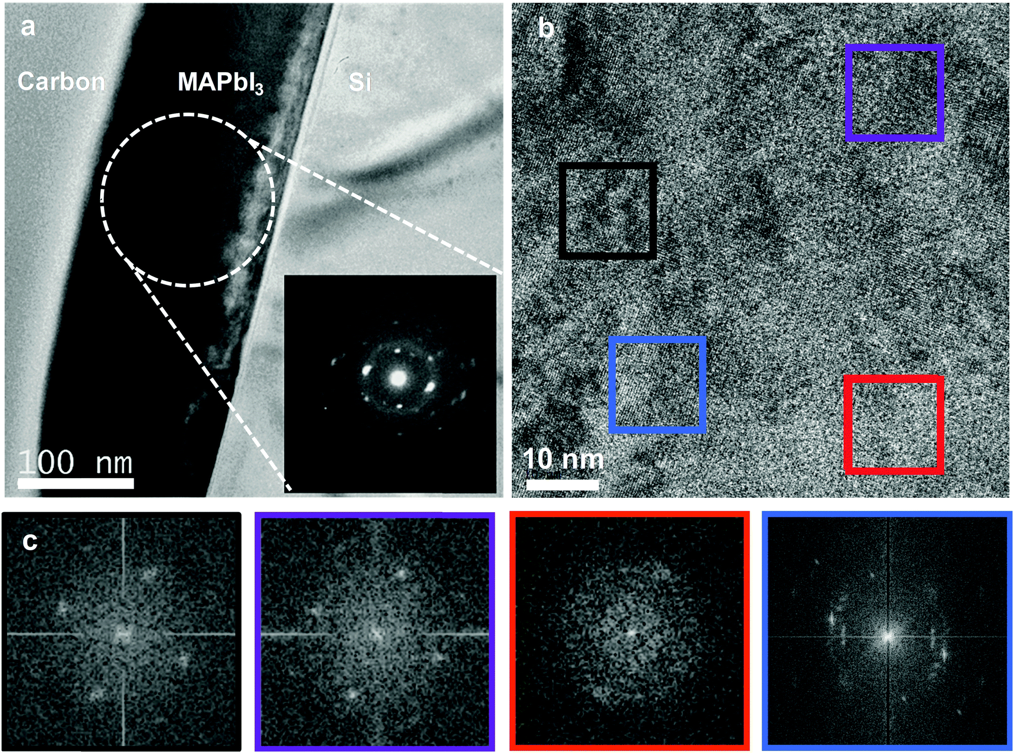 | ||
| Fig. 4 TEM electron diffraction analysis of MAPbI3 perovskite grains. (a) Cross-section image of single perovskite grain on Si〈100〉 substrate and selected area electron diffraction (SAED) pattern collected from the region indicated (inset). (b) Higher-magnification TEM and (c) fast Fourier transform (FFT) patterns generated across different regions of the grain shown in (b). | ||
To probe crystallinity at a deeper scale, a high-resolution TEM (HR-TEM) micrograph was collected from a 70 × 70 nm2 region using a low electron dose rate of ∼1–4 electrons Å−2 s−1, in line with previous reports34 (Fig. 4b). The micrograph shows a lack of lattice continuality in the tested area as indicated by the presence of domains and structural defects. Fast Fourier transform (FFT) patterns generated from various 10 × 10 nm2 regions of the HR-TEM micrograph are outlined by the coloured boxes in Fig. 4c and clearly demonstrate structural heterogeneity within a single grain. The regions marked by black and purple boxes possess near-identical diffraction patterns and are highly crystalline as indicated by the sharp diffraction spots. The identical d-spacing of the diffraction spots indicate a similarity in crystallinity and sub-grain crystallite orientation on the 10 × 10 nm2 scale. The highly crystalline regions marked by the black and purple boxes contrast with regions bound by the red and blue boxes. The markedly different patterns indicate the whole grain is not uniformly crystallized. The blue region is well-crystallised but shows the presence of more than one diffraction pattern. This can be a result of multi-grain overlap or can indicate the presence of structural defects such as micro-twins and/or dislocations that can provide additional strain relief.34 In contrast, the red box shows a much weaker pattern indicating a poorly-crystallised or amorphous region within the same grain. While amorphisation due to beam damage cannot be excluded, a lack of homogeneity in the amorphisation signature through the sample makes irradiation-induced amorphisation less plausible, and the local changes in crystallographic orientation, or twinning, are highly unlikely to arise from beam damage.34 These results reveal that each of these grain “entities” are in fact comprised of many sub-crystallites on a ∼10–100 nm scale above that of the unit cell but below that of a single grain. This scale of heterogeneity is consistent with recent reports showing lower symmetry domains below 20 nm35 and substantial spatial variation in the photo-response of polycrystalline perovskite devices even within each grain.15,36,37
Discussion
Our work reveals that strained regions are associated with increased fractions of charged defects and increased non-radiative decay, which has profound ramifications on our understanding of the impact of crystallinity on carrier recombination. Local strain is present in these halide perovskite thin-films as a result of the standard processing conditions. During crystallisation a MAPbI3 film is annealed at 100 °C in which the perovskite structure is nominally cubic, and then by cooling to room temperature it passes through a cubic-to-tetragonal phase transition (57 °C).38 Cooling through this phase transition results in spatially heterogeneous built-in strain and the formation of many tetragonal domains.34,39 The magnitude of the strain would depend on the dimensions and local environment of each domain, where some regions may be more or less constrained by neighbouring domains than others. These local environments could be established through inhomogeneous nucleation and growth, where differences in local substrate morphology, local concentration gradients, or intermediate phases40 during solution deposition would template heterogeneous growth. The presence of large super-grains sharing similar orientations suggests common growth mechanisms for some regions, which may result in longer-range strain effects. Consideration of the thermal expansion coefficient of MAPI341 and the temperature change (100 °C to room temperature) yields a uniaxial strain of ∼0.3%, which is similar to our observed values. The simultaneous spontaneous deformation (tetragonal distortion c/2a = 1.01 at 300 K) results in an anisotropic strain tensor that can be relieved through a combination of point and extended defects such as twin boundaries, which is established in oxide perovskites.42,43 We note that the vacancies themselves cannot cause the coherent compressive strain gradients that we observe: a vacancy concentration of even 1017 cm−3 would correspond to fewer than 1 defect in every 10![[thin space (1/6-em)]](https://www.rsc.org/images/entities/char_2009.gif) 000 unit cells, which is too dilute to cause the observed magnitude of strain.
000 unit cells, which is too dilute to cause the observed magnitude of strain.
Seeking deposition methods that minimise local strain fields will be critical for achieving devices approaching the radiative limits. This includes developing compositions and lower temperature processing methods that do not require the material to proceed through a phase transition during film formation. As an example, the FA-rich alloyed perovskites demonstrating the highest solar cell device performances to date are closer to cubic at room temperature44 and thus do not undergo a phase transition between annealing and room temperature; stabilising such cubic structures at room temperatures will be critical for development of new alloyed analogues. In fact, our measurements performed on the MA0.15FA0.79Cs0.06Pb(I0.85Br0.15)3 films (cf.Fig. 3) reveal that there is reduced local heterogeneity in these samples and that the long range super-grain features exist over a much longer distance than the MAPbI3 counterparts, consistent with a reduced impact of strain. Judicious choice of the solar cell or LED device contacts will also be critical, as these may induce additional strain during perovskite growth (if underneath the perovskite) or during contact deposition (on top of the perovskite). This may require careful matching of the lattice parameters of contact materials to the perovskite; this has not been an issue to date but may become critical when approaching the performance limits in which all strain-related defects must be eliminated. Finally, passivation treatments must target relieving strain either through steric design of chemically passivating molecules or through managing the concentrations and spatial distribution of defects.2,6,7
Our work has revealed that this strain-related heterogeneity proliferates across many length scales throughout the entire film, from long-range super-grain clusters, to grain-to-grain and sub-grain nanoscale variations. This suggests that we need to re-think the conception of a perovskite grain as a single crystalline entity, for example as viewed in electron microscopy. This highlights important new questions on nucleation and grain growth. The large impact of local strain on local optoelectronic properties also opens up the ability to manipulate perovskite optoelectronic behaviour through purposeful engineering of local strain fields in novel device structures. For example, the formation of large super-grain clusters with analogous orientation and facet control may have beneficial properties for carrier transport, and could be utilised in lateral or back-contact device structures. Furthermore, the large perturbations to the crystal symmetry may lead to a Rashba effect in the electronic structure, which will further influence carrier dynamics,45 and this could be induced on a local level such as at a heterojunction interface. Nevertheless, the exceptional performance of perovskites in spite of so many layers of disorder is remarkable. Their behaviour is akin to liquid metals, which have disordered structures, yet maintain excellent charge transport properties.46 This sentiment would also explain the high open-circuit voltages in devices even in the earliest stages of disordered crystallite formation.47
Conclusion
We have correlated synchrotron scanning μXRD measurements with local time-resolved photoluminescence measurements from MAPbI3 films on the same scan area, revealing that local strain leads to defects such as halide vacancies that are associated with local non-radiative decay. The strain is complex and manifests itself on multiple length scales, including on the tens of microns scale (many times larger than a “grain” as viewed in SEM) as well as on the tens of nanometres scale (sub-“grain”). We propose that the strain is built into the film during processing, in particular during cooling through the cubic-to-tetragonal phase transition following the standard annealing procedure. We identify that improved growth and passivation methods must target strain relief, for example by manipulating the local phase behaviour during growth or post-treatments which relieve constrained regions. Future developments and research will be required to solve open questions relating to how the strain-related defects directly lead to non-radiative recombination. For example, halide vacancies are positively charged and therefore attract electrons, but there is insufficient information available on capture-cross sections and trapping rates. Future work will also be required to consolidate our understanding of the complex relationships between physicochemical and optoelectronic properties, which would ultimately guide growth of films with optimal structural properties across all scales.Experimental methods
Sample preparation
All organic-based precursor salts were purchased from Dyesol. Unless otherwise stated, all other materials were purchased from Sigma-Aldrich. All film samples were prepared in and then stored in a nitrogen-filled glovebox until used. Prior to PL measurement, the samples were stored in a dry air desiccator for 24 hours to stabilize any photo-brightening effects.Glass cover slips (PL, micro-XRD measurements) or Si〈100〉 substrates (nano-XRD, TEM measurements) were washed sequentially with soap (Micro 90), de-ionized water, acetone, and isopropanol, and treated under oxygen plasma for 10 minutes. Thin films of MAPbI3 were solution-processed by employing a methylammonium iodide (MAI) and lead acetate Pb(Ac)2·3H2O precursor mixture with a hypophosporous acid (HPA) additive.24 MAI and Pb(Ac)2·3H2O were dissolved in anhydrous N,N-dimethylformamide at a 3:1 molar ratio with final concentration of 37 wt% and HPA added to a HPA:Pb molar ratio of ∼11%. The precursor solution was spin-coated at 2000 rpm for 45 seconds in a nitrogen-filled glovebox, and the substrates dried at room temperature for 10 minutes before annealing at 100 °C for 5 minutes.
The triple-cation-based perovskite MA0.15FA0.79Cs0.06Pb(I0.85Br0.15)3 samples were prepared by dissolving PbI2 (1.2 M, TCI), FAI (1.11 M), MABr (0.21 M) and PbBr2 (0.21 M, TCI) in a mixture of anhydrous DMF:DMSO (4:1, volume ratios) followed by addition of 5 volume percent from CsI (TCI, Japan) stock solution (1.5 M in DMSO). We then spin-coated the perovskite solution using a two-step program at 2000 and 4000 rpm for 10 and 40 seconds, respectively, and dripping 150 μL of chlorobenzene after 30 seconds. We then annealed the films at 100 °C for 1 hour.
Fiducial markers
The Au nanoplates were synthesized following a modified procedure reported by Gu et al.48 A 25 mL solution of ethylene glycol with 0.054 mmol of HAuCl4·4H2O was heated to 65 °C in a water bath for 20 min. Then, 0.1 M aniline solution in ethylene glycol was added to the heated HAuCl4 solution under mild stirring to acquire a 2:1 molar ratio of aniline to Au. This reaction was allowed to proceed for 3 hours without stirring leading to formation of triangular and hexagonal Au nanoplates with spherical nanoparticles as a byproduct. The nanoplates precipitated at the bottom of the vial while the supernatant mainly contained the spherical particles. The supernatant was gently removed without disturbing the precipitant and replaced with fresh ethanol. This was followed by two more rounds of precipitation to thoroughly clean the nanoplates in ethanol. Lastly, the ethanol was removed and the particles were dispersed in chlorobenzene (∼0.5–1 mL). The solution was sonicated for 30 seconds and spincoated on top of the perovskite samples at 1000 rpm for 60 seconds, resulting in a dispersion on the surfaces with a concentration of ∼1 particle cluster per 100 × 100 μm2.
Bulk X-ray diffraction measurements
Bulk X-ray diffractograms (cf. Fig. S1, ESI†) were collected from thin film samples using a PANalytical X’Pert Pro Multi-Purpose Diffractometer operated at 45 kV and 40 mA (Cu K-alpha radiation – 1.5418 Å) in Bragg–Brentango geometry. An Oxford Cryosystems PheniX cryostat was employed to measure while holding the sample at 240 K.Micro(confocal)-photoluminescence measurements
Confocal photoluminescence (PL) maps were acquired using a custom-built time-correlated single photon counting (TCSPC) confocal microscope (Nikon Eclipse Ti-E) setup with a 100× oil objective (Nikon CFI PlanApo Lambda, 1.45 NA). The cover slip samples were photo-excited through the glass-side using a 405 nm laser head (LDH-P-C-405, PicoQuant GmbH) with pulse duration of <90 ps, fluence of ∼0.1 μJ per cm2 per pulse, and a repetition rate of 0.5 MHz. The maps were acquired with a step size of 60 nm and a dwell time on each pixel of 20 ms. The PL from the sample was collected by the same objective and the resulting collimated beam passes through a long-pass filter with a cut-off at 416 nm (Semrock Inc., BLP01-405R-25) to remove any residual scattered or reflected excitation light. A single photon detecting avalanche photodiode (APD) (MPD PDM Series 50 mm) was used for the detection. The sample was scanned using a piezoelectric scanning stage. The measurements were acquired and intensity and average-lifetime maps extracted using the software SymphoTime 64 (PicoQuant GmbH).We note that the total light dose on each local region during the PL maps (<1 J cm−2) is much lower than that required to see light-induced changes in these samples.49,50 Furthermore, following the PL measurements, the samples were stored in vacuum bags before being loaded directly onto the chilled nitrogen flow for the XRD measurements (see below); control PL maps taken on films stored in a similar manner did not show any significant changes. This suggests that the illumination, storage and transport did not affect the samples.
Micro-X-ray diffraction measurements and analysis
X-ray microdiffraction data at the Advanced Light Source were collected on beamline 12.3.2.51 The samples were placed in reflective geometry at a 15° grazing incidence angle (Fig. S2, ESI†); we account for the associated increased beam footprint (2.5 μm × 9.6 μm) on the sample in our correlations. The substrate was cooled under continuously flowing nitrogen to 240 K (as measured by a thermocouple) with a Cryostream 700 Series from Oxford Cryosystems; we note that we observed similar qualitative results when measured at room temperature. This setup also protected the sample from condensation by immersing the sample with a protective sheath of dry nitrogen evaporate, and we subsequently did not observe any evidence of moisture-related degradation or hydrated crystalline species during the measurements. The 2D X-ray diffraction patterns were collected using a DECTRIS Pilatus 1 M hybrid pixel area detector placed at an angle of 50° with respect to the incident beam and at a distance about 160 mm from the sample. The energy of the incident beam was set to 10 keV (wavelength λ = 1.2398 Å). The diffraction patterns were analyzed using the X-ray Microdiffraction Analysis Software (XMAS) package.52 Experimental geometry was calibrated using an Al2O3 powder, in which the detector position and angular tilts with respect to the incident X-ray beam and sample were refined. An additional calibration on the sample themselves was performed on some of the data to minimize displacement errors due to the shallow incident angle of the X-ray beam onto the sample surface. The 2D diffraction patterns were then integrated over the azimuthal direction to obtain 1D diffractograms, from which radial peak profiles were obtained and strain and particle size were calculated. See ESI,† for details of further data extraction, fitting, image registration and correlation fits.Nano-X-ray diffraction measurements and analysis
Scanning nanofocus XRD measurements were conducted at the ID13 beamline at the European Synchrotron Radiation Facility. Samples were mounted on a xyz piezo stage and were illuminated in transmission geometry (Fig. S20, ESI†) with a monochromatic beam (λ ≈ 0.8377 nm, spot size ∼0.2 × 0.2 μm2). Diffraction images were collected using an Eiger X 4M detector (Dectris AG, Switzerland) with 2168 row pixels and 2070 column pixels (75 × 75 μm2 pixel size) and an exposure of 0.1 s per diffraction pattern (acquisition time of 0.1 s per diffraction pattern). The detector was placed 19.41 cm away from the sample. The detector position and geometry were calibrated by recording a diffraction pattern of the standard calibration material corundum (α-Al2O3). Samples were raster scanned over a 40 × 40 μm2 area with a step size of ∼400 nm. Measurements were performed under ambient conditions (lab temperature ∼24 °C, relative humidity ∼40%). The collected data consisted of 10201 diffraction images per scan area.
Diffraction data was analysed as in ref. 26. Briefly, after the construction of an average diffraction pattern for the diffraction collected across the entire scan area for the MAPbI3 and MA0.15FA0.79Cs0.06Pb(I0.85Br0.15)3 films, we create circular regions of interest (ROIs) around the 〈110〉 and 〈210〉 perovskite reflection rings, respectively. Diffraction spots in the ROI-restricted pattern of the scan were analyzed and used to perform grain clustering based on the azimuthal angle coordinate χp extracted from the center of each diffraction spot. We assume that diffraction spots that are adjacent both in spatial coordinates and in reciprocal space coordinates originate from the same grain. This clustering is performed based on the pairwise Euclidean distance between pixels. We used an empirically-determined threshold value for cutting the hierarchical tree. The dataset for the identification of the diffraction spots is bi-dimensional (pixel X and pixel Y), and the dataset for the identification of the super-grains is tri-dimensional (2 spatial coordinates X and Y, and the azimuthal angle). The area of each ‘super-grain’ is simply calculated as the number of pixels within the ‘super-grain’ multiplied by the area of a pixel in microns. This gives a collection of super-grains (clusters) that can be ordered in decreasing size (Fig. 3d). Spatial maps of the q position were obtained from the line profiles extracted for all the diffraction spots in the ROI for each super-grain.
Transmission electron microscopy
TEM and HRTEM were carried out using a JEOL FasTem-2010 instrument operating at 200 kV. Film thickness was measured from TEM cross sections. We kept the dose low and studied the reciprocity failure by keeping the dose constant and changing the exposure times. Low-dose TEM imaging was performed with an electron dose rate of ∼1–4 e Å−2 s−1, in line with previous reports.34 The diffraction patterns and HR-TEM images were recorded from previously unexposed regions of the sample and both selected area electron diffraction (SAED) and Fast Fourier Transform (FFT) analysis from the HR-TEM imaging confirmed the tetragonal structure of the MAPbI3 lattice. The crystal grains were examined in an ‘as-found’ orientation, without any attempt at crystal alignment that would have incurred further electron dose.First-principles simulations
Calculations were performed on MAPbI3 in the room-temperature tetragonal phase. First the unit cell (lattice vectors and internal positions) was optimized to within a force tolerance of 0.001 eV per Ångstrom as calculated using density functional theory (PBEsol functional including scalar-relativistic effects) within the code VASP. The valence electrons were expanded in a plane-wave basis set with a cutoff of 700 eV, and the k-point sampling was set to 6 × 6 × 4.The equilibrium crystal structure was then subject to compressive and tensile strain (up to 0.5%) along the 〈110〉 and 〈111〉 crystallographic orientations. Next, the formation of iodine vacancy defects was probed in a series of 5 structures for each value of strain (ε), with the defect energy calculated from:
| ΔED,ε = E[defect]ε − E[bulk]ε |
Author contributions
Samples were prepared by RB and MA-J, and fiducial alignment particles synthesised by FN. TWJ, AO, MS and GJW performed the micro-XRD measurements in conjunction with CVS, YL and NT, and the results were analyzed by BCD, TJ, CS and SDS. SDS performed and analysed the PL maps. The correlations between micro-XRD and PL maps were conducted by BCD, TJ and SDS. MA, SL, JEM and MB performed and analysed the nano-XRD measurements. AO performed the bulk XRD and TEM measurements. Y-KJ and AW performed the first-principles simulations. SDS coordinated and supervised the project. GJW supervised TWJ and BCD. VB supervised AO, MS and FN. RHF supervised MA. TWJ and SDS wrote the manuscript with contributions from other authors.Conflicts of interest
Samuel D. Stranks is a Co-Founder of Swift Solar Inc.Acknowledgements
TWJ acknowledges the Australian Renewable Energy Agency for a post-doctoral Fellowship. This project has received funding from the European Union's Seventh Framework Programme (PIOF-GA-2013-622630), the European Research Council (ERC) under the European Union's Horizon 2020 research and innovation programme (HYPERION, grant agreement No. 756962), and the Royal Society and Tata Group (UF150033). GJW acknowledges the support of a CSIRO Julius Career Fellowship. TWJ and GJW acknowledge travel funding provided by the International Synchrotron Access Program (ISAP) managed by the Australian Synchrotron, part of ANSTO, and funded by the Australian Government. This work made use of the Shared Experimental Facilities supported in part by the MRSEC Program of the National Science Foundation under award number MDR – 1419807. This work was supported in part by the Yonsei University Future-leading Research Initiative of 2017-22-0088. This research used resources of the Advanced Light Source, which is a DOE Office of Science User Facility under contract no. DE-AC02-05CH11231. We thank the European Synchrotron Radiation Facility (ESRF) for beamtime at the ID13 beamline and the beamline staff for measurement support. M. A.-J. thanks Nava Technology Limited, Cambridge Materials Limited and EPSRC (EP/M005143/1) for funding and technical support. AO acknowledges the NSF under Grant No. 1605406 (EP/L000202). M. A. received funding from The President of the UAE's Distinguished Student Scholarship Program (DSS), granted by the Ministry of Presidential Affairs. This work was also supported by a National Research Foundation of Korea (NRF) grant funded by the Korean government (MSIT) (No. 2018R1C1B6008728).References
- S. D. Stranks and H. J. Snaith, Nat. Nanotechnol., 2015, 10, 391–402 CrossRef CAS PubMed.
- W. S. Yang, B. W. Park, E. H. Jung, N. J. Jeon, Y. C. Kim, D. U. Lee, S. S. Shin, J. Seo, E. K. Kim, J. H. Noh and S. I. Seok, Science, 2017, 356, 1376–1379 CrossRef CAS PubMed.
- B. R. Sutherland and E. H. Sargent, Nat. Photonics, 2016, 10, 295–302 CrossRef CAS.
- O. D. Miller, E. Yablonovitch and S. R. Kurtz, IEEE J. Photovolt., 2012, 2, 303–311 Search PubMed.
- S. D. Stranks, ACS Energy Lett., 2017, 2, 1515–1525 CrossRef CAS.
- D. W. deQuilettes, S. Koch, S. Burke, R. K. Paranji, A. J. Shropshire, M. E. Ziffer and D. S. Ginger, ACS Energy Lett., 2016, 1, 438–444 CrossRef CAS.
- M. Abdi-Jalebi, Z. Andaji-Garmaroudi, S. Cacovich, C. Stavrakas, B. Philippe, J. M. Richter, M. Alsari, E. P. Booker, E. M. Hutter, A. J. Pearson, S. Lilliu, T. J. Savenije, H. Rensmo, G. Divitini, C. Ducati, R. H. Friend and S. D. Stranks, Nature, 2018, 555, 497–501 CrossRef CAS.
- R. Brenes, D. Guo, A. Osherov, N. K. Noel, C. Eames, E. M. Hutter, S. K. Pathak, F. Niroui, R. H. Friend, M. S. Islam, H. J. Snaith, V. Bulović, T. J. Savenije and S. D. Stranks, Joule, 2017, 1, 155–167 CrossRef CAS.
- I. L. Braly, D. W. deQuilettes, L. M. Pazos-Outón, S. Burke, M. E. Ziffer, D. S. Ginger and H. W. Hillhouse, Nat. Photonics, 2018, 12, 355–361 CrossRef CAS.
- C. Momblona, L. Gil-Escrig, E. Bandiello, E. M. Hutter, M. Sessolo, K. Lederer, J. Blochwitz-Nimoth and H. J. Bolink, Energy Environ. Sci., 2016, 9, 3456–3463 RSC.
- M. Saliba, T. Matsui, K. Domanski, J. Y. Seo, A. Ummadisingu, S. M. Zakeeruddin, J. P. Correa-Baena, W. R. Tress, A. Abate, A. Hagfeldt and M. Gratzel, Science, 2016, 354, 206–209 CrossRef CAS PubMed.
- M. A. Green and S. P. Bremner, Nat. Mater., 2017, 16, 23–34 CrossRef PubMed.
- D. W. deQuilettes, S. M. Vorpahl, S. D. Stranks, H. Nagaoka, G. E. Eperon, M. E. Ziffer, H. J. Snaith and D. S. Ginger, Science, 2015, 348, 683–686 CrossRef CAS PubMed.
- Z. Guo, J. S. Manser, Y. Wan, P. V. Kamat and L. Huang, Nat. Commun., 2015, 6, 7471 CrossRef CAS PubMed.
- S. Y. Leblebici, L. Leppert, Y. Li, S. E. Reyes-Lillo, S. Wickenburg, E. Wong, J. Lee, M. Melli, D. Ziegler, D. K. Angell, D. F. Ogletree, P. D. Ashby, F. M. Toma, J. B. Neaton, I. D. Sharp and A. Weber-Bargioni, Nat. Energy, 2016, 1, 16093 CrossRef CAS.
- S. D. Stranks, V. M. Burlakov, T. Leijtens, J. M. Ball, A. Goriely and H. J. Snaith, Phys. Rev. Appl., 2014, 2, 034007 CrossRef.
- A. M. Stoneham, Rep. Prog. Phys., 1981, 44, 1251 CrossRef.
- J. R. Haynes and J. A. Hornbeck, Phys. Rev., 1955, 100, 606–615 CrossRef CAS.
- E. M. Hutter, G. E. Eperon, S. D. Stranks and T. J. Savenije, J. Phys. Chem. Lett., 2015, 6, 3082–3090 CrossRef CAS PubMed.
- Y. Yamada, M. Endo, A. Wakamiya and Y. Kanemitsu, J. Phys. Chem. Lett., 2015, 6, 482–486 CrossRef CAS PubMed.
- J. Zhao, Y. Deng, H. Wei, X. Zheng, Z. Yu, Y. Shao, J. E. Shield and J. Huang, Sci. Adv., 2017, 3, eaao5616 CrossRef PubMed.
- D. P. McMeekin, Z. Wang, W. Rehman, F. Pulvirenti, J. B. Patel, N. K. Noel, M. B. Johnston, S. R. Marder, L. M. Herz and H. J. Snaith, Adv. Mater., 2017, 1607039, DOI:10.1002/adma.201607039.
- J. T.-W. Wang, Z. Wang, S. Pathak, W. Zhang, D. W. deQuilettes, F. Wisnivesky-Rocca-Rivarola, J. Huang, P. K. Nayak, J. B. Patel, H. A. Mohd Yusof, Y. Vaynzof, R. Zhu, I. Ramirez, J. Zhang, C. Ducati, C. Grovenor, M. B. Johnston, D. S. Ginger, R. J. Nicholas and H. J. Snaith, Energy Environ. Sci., 2016, 9, 2892–2901 RSC.
- W. Zhang, S. Pathak, N. Sakai, T. Stergiopoulos, P. K. Nayak, N. K. Noel, A. A. Haghighirad, V. M. Burlakov, D. W. deQuilettes, A. Sadhanala, W. Li, L. Wang, D. S. Ginger, R. H. Friend and H. J. Snaith, Nat. Commun., 2015, 6, 10030 CrossRef CAS PubMed.
- R. L. Z. Hoye, P. Schulz, L. T. Schelhas, A. M. Holder, K. H. Stone, J. D. Perkins, D. Vigil-Fowler, S. Siol, D. O. Scanlon, A. Zakutayev, A. Walsh, I. C. Smith, B. C. Melot, R. C. Kurchin, Y. Wang, J. Shi, F. C. Marques, J. J. Berry, W. Tumas, S. Lany, V. Stevanović, M. F. Toney and T. Buonassisi, Chem. Mater., 2017, 29, 1964–1988 CrossRef CAS.
- S. Lilliu, T. G. Dane, M. Alsari, J. Griffin, A. T. Barrows, M. S. Dahlem, R. H. Friend, D. G. Lidzey and J. E. Macdonald, Adv. Funct. Mater., 2016, 26, 8221–8230 CrossRef CAS.
- J. Feng, APL Mater., 2014, 2, 081801 CrossRef.
- G. K. Williamson and W. H. Hall, Acta Metall., 1953, 1, 22–31 CrossRef CAS.
- M. Saliba, T. Matsui, J. Y. Seo, K. Domanski, J. P. Correa-Baena, M. K. Nazeeruddin, S. M. Zakeeruddin, W. Tress, A. Abate, A. Hagfeldt and M. Gratzel, Energy Environ. Sci., 2016, 9, 1989–1997 RSC.
- D. W. deQuilettes, S. Jariwala, S. Burke, M. E. Ziffer, J. T. W. Wang, H. J. Snaith and D. S. Ginger, ACS Nano, 2017, 11, 11488–11496 CrossRef CAS PubMed.
- W.-J. Yin, T. Shi and Y. Yan, Appl. Phys. Lett., 2014, 104, 063903 CrossRef.
- M.-H. Du, J. Phys. Chem. Lett., 2015, 6, 1461–1466 CrossRef CAS PubMed.
- F. De Angelis and A. Petrozza, Nat. Mater., 2018, 17, 383–384 CrossRef CAS.
- M. U. Rothmann, W. Li, J. Etheridge and Y.-B. Cheng, Adv. Energy Mater., 2017, 7, 1700912 CrossRef.
- A. N. Beecher, O. E. Semonin, J. M. Skelton, J. M. Frost, M. W. Terban, H. Zhai, A. Alatas, J. S. Owen, A. Walsh and S. J. L. Billinge, ACS Energy Lett., 2016, 1, 880–887 CrossRef CAS.
- Y. Kutes, Y. Zhou, J. L. Bosse, J. Steffes, N. P. Padture and B. D. Huey, Nano Lett., 2016, 16, 3434–3441 CrossRef CAS PubMed.
- J. L. Garrett, E. M. Tennyson, M. Hu, J. Huang, J. N. Munday and M. S. Leite, Nano Lett., 2017, 17, 2554–2560 CrossRef CAS PubMed.
- T. Baikie, Y. N. Fang, J. M. Kadro, M. Schreyer, F. X. Wei, S. G. Mhaisalkar, M. Graetzel and T. J. White, J. Mater. Chem. A, 2013, 1, 5628–5641 RSC.
- S. M. Vorpahl, R. Giridharagopal, G. E. Eperon, I. M. Hermes, S. A. L. Weber and D. S. Ginger, ACS Appl. Energy Mater., 2018, 1, 1534–1539 CrossRef CAS.
- J. Cao, X. Jing, J. Yan, C. Hu, R. Chen, J. Yin, J. Li and N. Zheng, J. Am. Chem. Soc., 2016, 138, 9919–9926 CrossRef CAS PubMed.
- F. Brivio, J. M. Frost, J. M. Skelton, A. J. Jackson, O. J. Weber, M. T. Weller, A. R. Goñi, A. M. A. Leguy, P. R. F. Barnes and A. Walsh, Phys. Rev. B: Condens. Matter Mater. Phys., 2015, 92, 144308 CrossRef.
- G. Arlt, J. Mater. Sci., 1990, 25, 2655–2666 CrossRef CAS.
- H. Andreas, L. Dongkyu, G. Er-Jia, L. M. Tricia, R. P. Jonathan and L. Ho Nyung, J. Phys.: Condens. Matter, 2017, 29, 493001 CrossRef PubMed.
- M. T. Weller, O. J. Weber, J. M. Frost and A. Walsh, J. Phys. Lett., 2015, 6, 3209–3212 CAS.
- S. D. Stranks and P. Plochocka, Nat. Mater., 2018, 17, 381–382 CrossRef CAS PubMed.
- T. E. Faber and J. M. Ziman, Philos. Mag., 1965, 11, 153–173 CrossRef CAS.
- M. Alsari, O. Bikondoa, J. Bishop, M. Abdi-Jalebi, L. Y. Ozer, M. Hampton, P. Thompson, M. T. Hörantner, S. Mahesh, C. Greenland, J. E. Macdonald, G. Palmisano, H. J. Snaith, D. G. Lidzey, S. D. Stranks, R. H. Friend and S. Lilliu, Energy Environ. Sci., 2018, 11, 383–393 RSC.
- Z. Guo, Y. Zhang, Y. DuanMu, L. Xu, S. Xie and N. Gu, Colloids Surf., A, 2006, 278, 33–38 CrossRef CAS.
- R. Brenes, C. Eames, V. Bulovic, M. S. Islam and S. D. Stranks, Adv. Mater., 2018, 30, e1706208 CrossRef PubMed.
- D. W. deQuilettes, W. Zhang, V. M. Burlakov, D. J. Graham, T. Leijtens, A. Osherov, V. Bulovic, H. J. Snaith, D. S. Ginger and S. D. Stranks, Nat. Commun., 2016, 7, 11683 CrossRef CAS PubMed.
- M. Kunz, N. Tamura, K. Chen, A. A. MacDowell, R. S. Celestre, M. M. Church, S. Fakra, E. E. Domning, J. M. Glossinger, J. L. Kirschman, G. Y. Morrison, D. W. Plate, B. V. Smith, T. Warwick, V. V. Yashchuk, H. A. Padmore and E. Ustundag, Rev. Sci. Instrum., 2009, 80, 035108 CrossRef PubMed.
- N. Tamura, in Strain and Dislocation Gradients from Diffraction. Spatially-Resolved Local Structure and Defects, ed. R. Barabash and G. Ice, Imperial College Press, London, 2014, pp. 125–155 Search PubMed.
Footnotes |
| † Electronic supplementary information (ESI) available. See DOI: 10.1039/c8ee02751j |
| ‡ These authors contributed equally. |
| This journal is © The Royal Society of Chemistry 2019 |