Accelerated charge transfer via a nickel tungstate modulated cadmium sulfide p–n heterojunction for photocatalytic hydrogen evolution
Received
29th December 2018
, Accepted 12th March 2019
First published on 13th March 2019
Abstract
Improving the efficiency of charge separation is an important aspect in photocatalysis. With NiWO4 modulation, the results of the Mott–Schottky test, short fluorescence lifetime (1.87 ns), faster electron transfer rate constant (KET = 2.82 × 10⁸ s−1), larger efficiency of electron injection (ηinj = 52.7%), high photocurrent response, smaller transfer resistance (Rfilm = 2785 Ω cm2) and reaction resistance (Rct = 1.74 Ω cm2) showed that a new interface electric field was established and a more effective thermodynamic charge transfer path was formed. This evidence greatly supported the fact that the separation and transfer of space charges over CdS p–n were accelerated via NiWO4 modulation. The [CdS/NiWO4 (30%)] sample had the best H2 production performance, namely, the maximum H2 production in 5 hours was 757 μmol, which was 7.35 times higher than that of pure CdS nanorods. Moreover, a series of characterization results also showed that the NiWO4 decorated CdS p–n heterojunction improved the efficiency of photo-generated charge separation and the SEM, XRD, TEM, EDX, XPS, UV-vis DRS, transient fluorescence, electro-chemistry etc. results were in good agreement with each other.
1. Introduction
The continuous depletion of fossil energy has caused mankind to face two major problems: energy shortage and environmental pollution.1–3 These two issues have posed tremendous threats to the survival and development of human beings. Solar energy is a kind of sustainable clean energy.4 Therefore, how to make good use of solar energy and improve the efficiency of energy conversion are the key to solving the energy crisis and environmental pollution problems. At present, photocatalytic technology is considered as an effective countermeasure, which can continuously convert low-density solar energy into chemical energy through photochemical reactions and has the advantages of low cost and environmental friendliness. It exhibits a very wide range of applications, such as in dye-sensitized solar cells,5 photocatalytic degradation of pollutants,6 photocatalytic cleavage of water to H2,7 photoelectrochemical cathodic protection8 and photocatalytic reduction of CO2.9,10
In 1972, Fujishima and Honda discovered that TiO2 can decompose water into H2 and O2 under ultraviolet light,11 and since then a large number of scientists have focused their attention on semiconductor photocatalysts such as ZnO,12 CdS,13,14 BiVO4,15,16 and Ag3PO4.17 In addition to having an appropriate band gap energy level, an ideal semiconductor should have low cost, readily available materials, high stability, and be non-toxic, as well as exhibit efficient use of solar energy. However, few materials can satisfy the above conditions at the same time. For example, GaAs,18 PbS,19 and CdS are toxic, and they are prone to photo-corrosion and poor stability in aqueous solutions. ZnO is unstable in aqueous solution because it easily dissolves in water and can form Zn(OH)2 on the surface of ZnO, thereby passivating the photocatalyst. The conduction band (CB) of Fe2O3,20 SnO2 (ref. 21) and WO3 (ref. 22 and 23) is located in the lower part of the reversible hydrogen potential, which means that these materials need to be subjected to external bias to complete the hydrolysis reaction. However, photocatalytic technology faces many problems in practical applications, for example, how to increase the light absorption range of the photoelectric conversion material, the separation ability of the photoelectron–hole, and the stability of the photocatalytic catalytic performance.24 Through extensive research, scientists have found that constructing an interface heterojunction system is an effective method to improve the separation efficiency of photogenerated electrons and holes.25 The existence of these electric fields can increase the efficiency of separation of photogenerated electrons and holes and improve the photocatalytic properties.26
CdS has become a research hotspot in the field of photocatalysis in recent years due to its characteristics of visible light response and high cost performance. It has also become a hotspot in the field of photoelectrocatalysis. It is the ideal bandgap of CdS and the suitable conduction band (CB) position that satisfy the thermodynamic and kinetic requirements of photocatalytic water splitting.27 However, the lifetime of carriers generated by CdS itself is short and the redox reaction cannot be completed well. When the photogenerated holes are generated on the surface of CdS, if they cannot react with the surrounding sacrificial reagents or rapidly transfer to other substances, they will quickly oxidize CdS, resulting in rapid photo-corrosion28 and rapid crystal structure collapse. The photocatalytic performance also deteriorates.
Therefore, in order to improve the stability and photocatalytic performance of the CdS photocatalyst, many researchers have extensively applied various nano-morphologies of CdS semiconductor-based materials to the field of photocatalysis: (1) CdS hollow spheres: Zhang J. L. and Xing M. Y. et al. reported the MnOx@CdS/CoP hollow sphere photocatalyst, which was loaded with two cocatalysts (inside MnOx and outside CoP) for enhancing photocatalytic H2 evolution activities.29 Han J. and Wang M. G. et al. prepared CdS/TiO2 hollow sphere heterojunction photocatalysts to improve the photocatalytic activity.30 (2) CdS nanorods: Li Z. Y. and Liang Q. et al. synthesized highly stable CdS@UIO-66-NH2 core–shell nanorods for enhancing photocatalytic activity.31 Zeng R. C. and Feng C. et al. prepared MoS2 cluster modified CdS nanorods through a one-pot solvothermal method at lower temperature.32 (3) CdS nanowires: Yu J. G. and Zhang J. Y. et al. prepared a CdS/g-C3N4 core/shell nanowire hybrid system by solvothermal and chemisorption methods.28 (4) CdS quantum dots: Shi J. W. and Zou Y. J. et al. reported the study on CdS QD decorated WS2/CN 2D/2D nanosheets for water splitting.33 Wang X. C. and Zheng D. D. reported the integration of CdS quantum dots on hollow graphitic carbon nitride nanospheres for hydrogen evolution.34 (5) CdS nanoparticles: Fang P. F. and Wang H. M. et al. reported the study on WO3&WS2 nanorods coupled with CdS nanoparticles for hydrogen evolution.35 There are also some researchers who constructed a p–n type heterojunction36 by forming a built-in electric field from the n-type semiconductor to the p-type CdS between the two semiconductors, thereby accelerating the separation of electrons and holes and effectively suppressing the recombination of the charges.
NiWO4 has a characteristic wolframite structure with a monoclinic unit cell and space group,37 suitable band gap energy (2.20 eV),38 sufficient chemical and thermal stability, good quantum size effect, and excellent catalytic performance.39 It is these properties that have attracted extensive attention and research in the field of photocatalysis, making it an ideal catalyst for photocatalytic decomposition of water to produce H2. However, there are few reports on the use of the NiWO4 photocatalyst for H2 production from water splitting.
In this paper, we succeeded in constructing an efficient photocatalytic H2 production system of CdS/NiWO4. The first step is to synthesize CdS nanorods, and then load NiWO4 to the surface of the CdS nanorods through a simple hydrothermal reaction. In the meantime, the p–n junction is formed between the p-type NiWO4 (ref. 40) and n-type CdS, which accelerates the transfer of electrons and holes. As a result, the photocatalytic H2 production rate is greatly improved.
2. Experimental section
2.1 Photocatalyst preparation
2.1.1 Preparation of CdS nanorods.
A certain amount of Cd(NO3)2·6H2O and NH2CSNH2 are dissolved in 50 ml of ethylenediamine, and magnetically stirred for 30 minutes. Subsequently, the solution is transferred to an 80 ml polytetrafluoroethylene autoclave and heated to 160 °C for 48 h. After the reaction is completed and cooled to room temperature, the sample is obtained by centrifugation. Then, the precipitate is washed with distilled water and ethanol three times and dried at 60 °C for 10 hours.
2.1.2 Preparation of CdS/NiWO4 photocatalysts.
CdS/NiWO4 with different contents of NiWO4 [m(NiWO4)/m(CdS) × 100% = 5, 10, 30, 50 and 70] are prepared by a solvothermal method. Taking the preparation of the [CdS/NiWO4 (50%)] catalyst as an example, in a typical synthesis of the composite catalysts, firstly, 200 mg of the above-prepared CdS nanorods are added to a 100 ml beaker containing 60 ml of DI water and sonicated for 20 minutes. Soon afterwards, 77.46 mg of NiCl2·6H2O and 107.5 mg Na2WO4·6H2O are added to the above solution. After magnetic stirring for 30 minutes, the above solution is transferred to a 100 mL autoclave and heated to 130 °C for 12 h. Finally, after cooling down to room temperature, the sample is obtained by centrifugation, washing and drying. The other catalysts with different percentages NiWO4 are also prepared in the same way. We use [CdS/NiWO4 (x%)] (x = 5, 10, 30, 50, 70) to represent these samples.
2.2 Photocatalytic H2 measurements
We use 62 ml reaction bottles and a PCX50A Discover (Perfectlight, Beijing) for photocatalytic H2 production measurements. The specific steps are as follows: first of all, 20 mg of the sample, 30 ml of 10 vol% lactic acid and a magnetic stir bar are added to the reaction bottle. Then, after stirring for 5 minutes, we put the reaction bottle into the ultrasonic cleaner for sonication for 10 minutes. Subsequently, the system is ventilated with N2 for about 30 min to remove O2. Ultimately, we place the reactor on the multi-channel reaction system and extract 0.5 ml of gas to analyze through gas chromatography (Tianmei GC7900, TCD, 13× column, N2 as the carrier). We use the external standard method to calculate the amount of H2 produced.
Next, we test the apparent quantum efficiency (AQE) of the [CdS/NiWO4 (30%)] composite catalyst. The specific steps are as follows: 20 mg of the [CdS/NiWO4 (30%)] catalyst is placed in a 62 ml quartz reaction flask containing 30 ml of 10% lactic acid solution, then the oxygen in the bottle is replaced with N2 for 10 minutes and ultrasonic treatment is conducted for 10 minutes. A 300 W Xe lamp light source (CEL-HXF300) with 400, 420, 450, 475, 500, 520, 550 and 600 nm band pass filters is used as the light source to irradiate the reaction solution for 1 h separately. A PL-MW200 photoradiometer (Perfect Light) is used to measure the photon flux of the incident light. Based on eqn (1), the AQE at different wavelengths is calculated.
| |  | (1) |
2.3 Photoelectrochemical measurements
Photoelectrochemistry experiments are conducted on an electrochemical workstation (VersaSTAT4-400, AMETEK) using a homemade standard three-electrode cell, whose reference electrode, counter electrode and working electrode are respectively a saturated calomel electrode (SCE), Pt electrode and FTO (1 × 2 cm2) drop-coating homogeneous catalyst. The electrolyte is a Na2SO4 aqueous solution (0.2 mol L−1). A 300 W xenon lamp with a cut-off filter of 420 nm is used as the light source. The Mott–Schottky plot is recorded at 5 kHz frequency in the dark. The potential ranges from −1.5 to 2.0 V (vs. SCE).
2.4 Characterization
The crystalline structure, element composition and UV-vis diffuse reflectance spectra are respectively measured using an X-ray diffractometer (XRD, Rigaku RINT-2000), X-ray photoelectron spectroscope (XPS, ESCALAB 250Xi) and UV-2550 (Shimadzu) spectrometer (BaSO4 as the reference). The images of sample morphology are obtained using a field-emission scanning electron microscope (FESEM, JSM-6701F) and a transmission electron microscope (TEM, Tecnai G2-TF30). The nitrogen adsorption–desorption isotherms are measured at 77 K with an ASAP 2020 M instrument and analyzed using the Brunauer–Emmett–Teller (BET) equation. The pore size distribution plots are obtained by the Barrett–Joyner–Halenda (BJH) model. The photoluminescence (PL) emission spectra and time-resolved PL (TRPL) spectra are detected using a FluoroMAX-4 spectrometer (Horiba, France).
3. Results and discussion
3.1 XRD, SEM, and TEM analysis
3.1.1 XRD analysis.
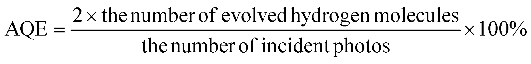
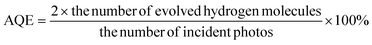
Fig. 1 shows the XRD patterns of the samples. In Fig. 1(A), in order to more intuitively observe and analyze the phase and crystallinity of the samples, we select the [CdS/NiWO4 (70%)] sample for analysis. It can be seen that in the characteristic peaks of the [CdS/NiWO4 (70%)] sample, not only the characteristic peaks of CdS but also the characteristic peaks of NiWO4 can be indexed. Through further observation, it can be observed that there are seven main sharp peaks at 2Θ = 24.85, 26.48, 28.24, 36.58, 43.78, 47.77 and 51.88°, matching well with the corresponding lattice faces of (100), (330), (101), (102), (110), (103) and (112), respectively (CdS with a space group of P63mc (no. 186), JCPDS no. 65-3414),42,43 and that there are four peaks located at 19.29, 31.11, 36.58 and 54.60°, which are consistent with the monoclinic NiWO4 phase (JCPDS no. 15-0755) with a space group of P2/c (no. 13) and correspond to the (100), (−111), (002) and (−202) planes, respectively. The three strong peaks of CdS and NiWO4 are obvious, and there are basically no other impurity peaks. Fig. 1(B) shows the XRD patterns of [CdS/NiWO4 (x%)] (x = 5, 10, 30, 50, 70). When the content of NiWO4 is gradually increased, the intensity of the characteristic peak of NiWO4 in the XRD pattern is also gradually enhanced, especially that of the 31.11° characteristic peak, demonstrating that the content of NiWO4 loaded on the CdS/NiWO4 is also gradually increasing.
 |
| | Fig. 1 The XRD patterns of (A) CdS/NiWO4 (70%) and JCPDS of CdS and NiWO4; (B) the XRD patterns of [CdS/NiWO4 (x%)] (x = 5, 10, 30, 50, 70). | |
3.1.2 SEM analysis.
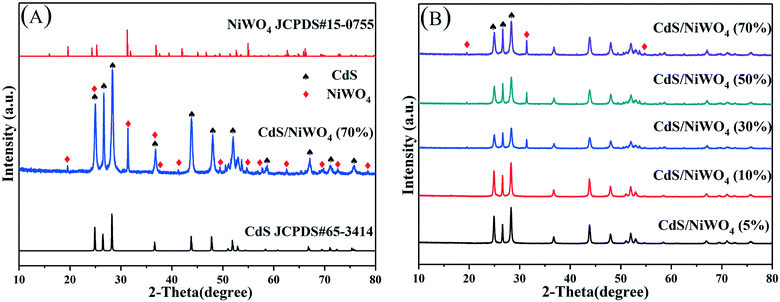
The morphology of CdS nanorods and [CdS/NiWO4 (30%)] is examined by SEM, the results of which are utilized to offer more intuitive information about the space shape, size, sample distribution of samples and so on. Fig. 2(A) and (B) show the SEM photographs of CdS nanorods at low magnification and high magnification, respectively. It can be clearly seen that the CdS nanorods are uniformly dispersed, with a size distribution of approximately 1 μm and a relatively smooth surface. Fig. 2(C) and (D) show the SEM images of [CdS/NiWO4 (30%)] at low magnification and high magnification, respectively. It can be found that the comparatively smooth surface of CdS nanorods becomes rough, and that there are many plate-like structures adhering to the surface of the CdS nanorods, manifesting that NiWO4 successfully attached to the surface of CdS nanorods, which can be verified by further TEM characterization.
 |
| | Fig. 2 SEM images: (A and B) CdS nanorods; (C and D) CdS/NiWO4 (30%). | |
3.1.3 TEM analysis.
TEM and HRTEM characterizations of the samples are of great importance in increasing the understanding of the internal structure and the morphology after the loading of NiWO4. In Fig. 3(A), we can further see that the CdS nanorods are uniformly dispersed, and the surface is relatively smooth, which is consistent with the XRD and the SEM results. On further observation of the HRTEM image in Fig. 3(B), the lattice spacing in the middle of two adjacent lattice planes is about 0.336 nm,27 which matches with the (002) lattice plane of CdS. Fig. 3(C and D) show the TEM images of [CdS/NiWO4 (30%)] at different magnifications from low to high. It is very clear that there is a sheet-like structure attached to the surface of the CdS nanorod. This is in agreement with the SEM image in Fig. 2(D). Further analysis of the HRTEM image in Fig. 3(E) shows that the lattice spacings in the middle of two adjacent lattice planes are about 0.336 and 0.245 nm,29 which matched the (002) lattice plane of CdS (ref. 27) and the (002) lattice plane of the monoclinic NiWO4,43 respectively. Fig. 3(F) shows the energy dispersive X-ray spectroscopy (EDX) spectrum of [CdS/NiWO4 (30%)] and the results demonstrate the presence of S, Cd, Ni, W and O elements.
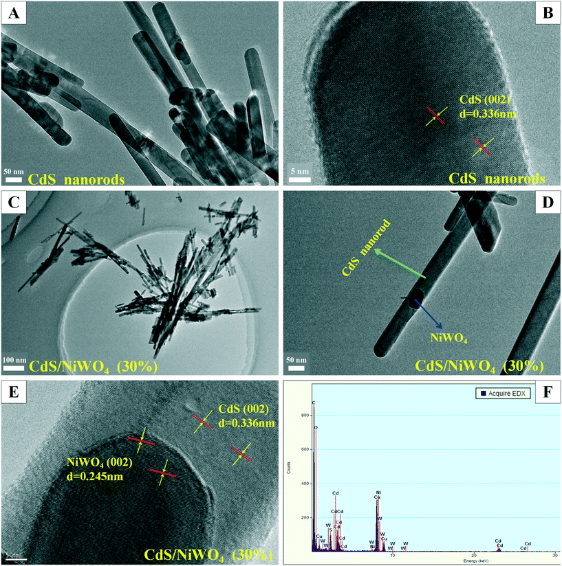 |
| | Fig. 3 (A and B) TEM and HRTEM images of CdS nanorods, (C–E) TEM and HRTEM images of [CdS/NiWO4 (30%)] and (F) EDX spectrum of [CdS/NiWO4 (30%)]. | |
3.2 XPS, BET, and UV-vis DRS analysis
3.2.1 XPS analysis.
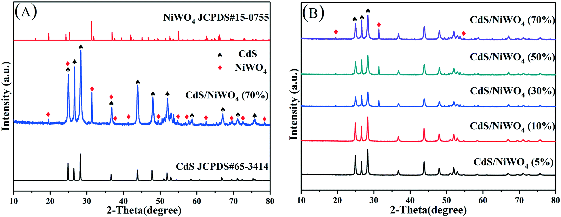
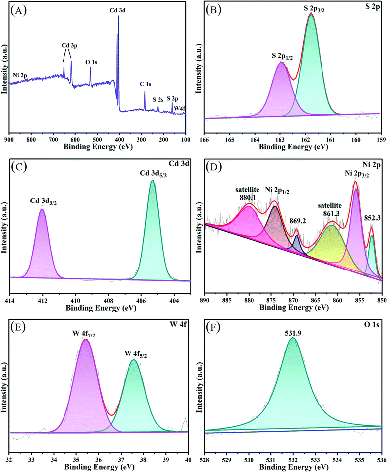
In order to further understand the element composition of the sample and the valence of each element, XPS studies on as-prepared [CdS/NiWO4 (30%)] are carried out so that we can obtain deeper insights. From the survey spectrum (Fig. 4(A)), we can find that the composite catalyst mainly consists of S, Cd, Ni, W and O elements. It can be seen that the S 2p spectrum (Fig. 4(B)) can be deconvoluted into two peaks including 161.76 eV for S 2p3/2 and 162.94 eV for S 2p1/2,44 and that the Cd 3d spectrum (Fig. 4(C)) can be resolved into two peaks located at 412.05 and 405.26 eV, which are ascribed to Cd 3d5/2 and Cd 3d3/2, respectively.45 In the Ni 2p spectrum in Fig. 4(D), it can be seen that there are six distinct characteristic peaks in the Ni spectrum, which belong to the Ni 2p3/2 and Ni 2p1/2 area, respectively. Further observation of the Ni 2p spectrum reveals that there are three distinct characteristic binding energy peaks located in the Ni 2p3/2 region. The three peaks are located at 852.3, 855.9 and 861.3 eV, which matched the Niδ+ in NiWO4, the Ni2+ species oxidation state and the satellite peak, respectively. Similarly, in the Ni 2p1/2 region, three peaks are located at 869.2, 874.2 and 880.1 eV, which originated from the Niδ+ in NiWO4, the Ni2+ species oxidation state and the satellite peak.46 In Fig. 4(E), the W 4f spectrum can be deconvoluted into well-resolved spin orbit split doublet peaks at 35.7 and 37.8 eV,37,47 which correspond to W 4f7/2 at 35.7 eV and W 4f5/2 at 37.8 eV, with a spin energy separation of 2.1 eV which is consistent with the previous report for W6+.37 Besides, both the W 4f7/2 peak at 35.7 eV and the Ni 2p3/2 peak at 855.9 eV demonstrate the formation of a Ni tungstate binary metal oxide. From the O 1s spectrum in Fig. 4(F), we can see that there is a major peak located at 531.9 eV,47 which is ascribed to the lattice oxygen in the NiWO4 phase indicating the presence of NiWO4.47
 |
| | Fig. 4 XPS patterns of the [CdS/NiWO4 (30%)] sample. (A) Survey, (B) S 2p, (C) Cd 3d, (D) Ni 2p, (E) W 4f and (F) O 1s scan spectra. | |
3.2.2 BET analysis.
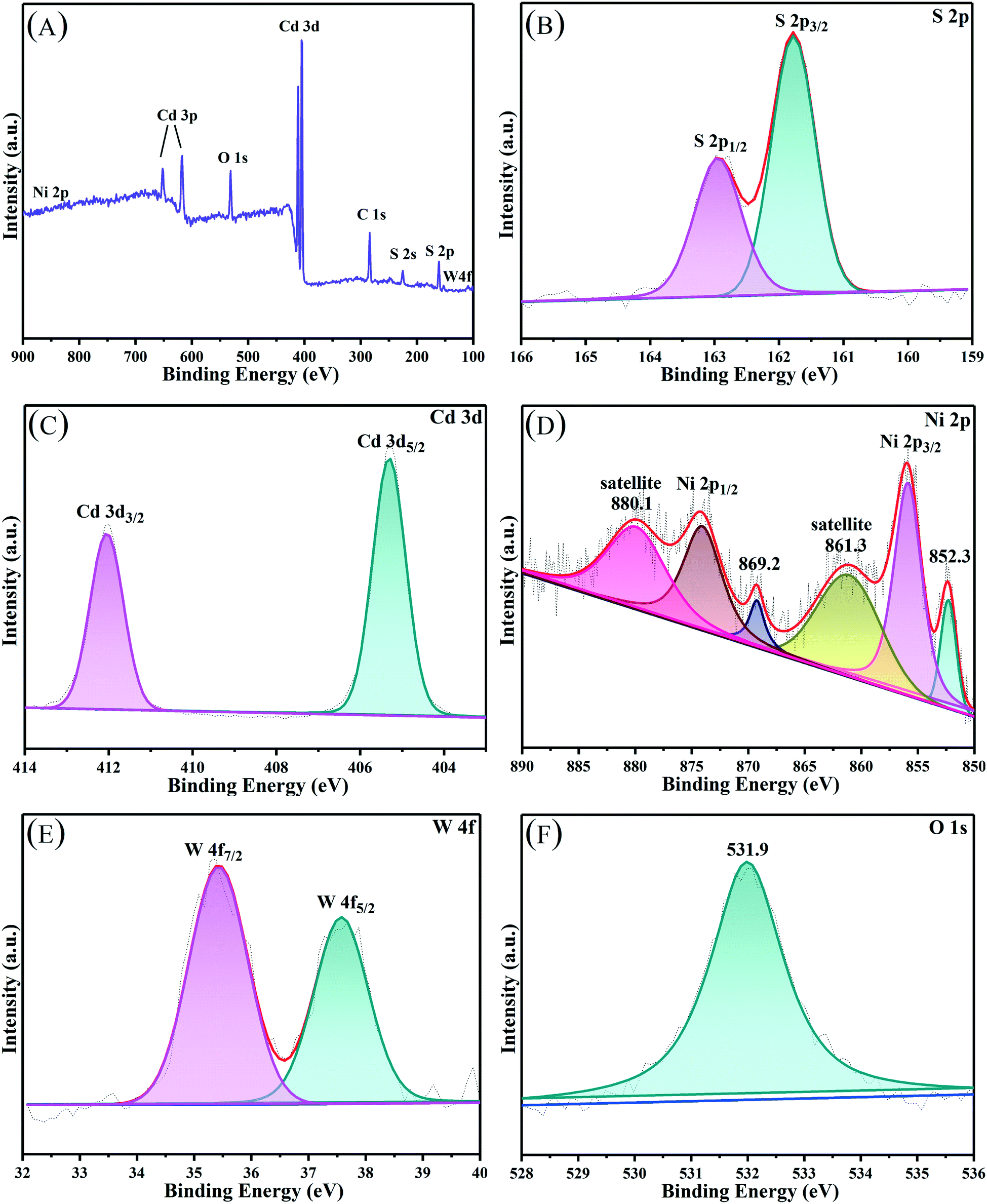
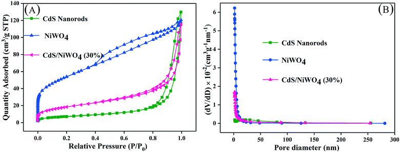
The physical adsorption properties of the samples are of great importance not only for the realization of improved sample performance, but also for affecting the catalytic reaction. The adsorption and desorption properties of the samples rely on their specific surface area, pore volume and pore size. In order to obtain the nitrogen adsorption and desorption isothermal curves, pore size distribution curves and physical adsorption desorption performance parameters of the samples, we utilize the ASAP 2020 M instrument at 77 K to carry out the experiment, whose results are shown in Fig. 5(A and B) and Table 1. From Fig. 5(A), we can observe that the adsorption/desorption curves of CdS nanorods, NiWO4 and [CdS/NiWO4 (30%)] belong to the type IV isotherm, whose hysteresis loop is of the H3 type. We can draw a conclusion from Fig. 5(B) that the three materials are mesoporous materials on the basis of the pore size distribution curve and the average pore size.
 |
| | Fig. 5 (A) The N2 adsorption–desorption isotherms and (B) corresponding pore size distribution curves. | |
Table 1 The physical adsorption performance parameters
| Samples |
S
BET
(m2 g−1) |
Pore volumeb (cm3 g−1) |
Average pore sizeb (nm) |
|
Obtained from the BET method.
Relative pressure (P/P0) was 0.99.
|
| CdS |
27 |
0.20 |
24.0 |
| NiWO4 |
190 |
0.18 |
4.1 |
| CdS/NiWO4 (30%) |
66 |
0.18 |
11.1 |
On further analysis of Table 1, we can see that the specific surface area of pure CdS nanorods and NiWO4 is 27 and 190 m2 g−1, respectively. At the same time, we can see that the pure CdS nanorods have a larger average pore size, reaching 24.0 nm, and that NiWO4 has a minimum average pore size of 4.1 nm. When 30% of NiWO4 is loaded onto the surface of CdS nanorods, the specific surface area of the composite catalyst [CdS/NiWO4 (30%)] is between those of CdS nanorods and NiWO4, which indicates that NiWO4 has been successfully loaded onto the surface of CdS nanorods, which is beneficial to the photocatalytic reactions.
3.2.3 UV-vis DRS analysis.
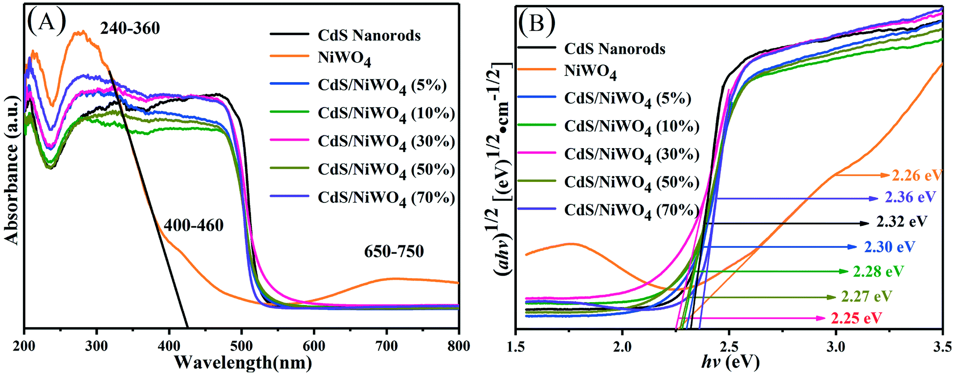
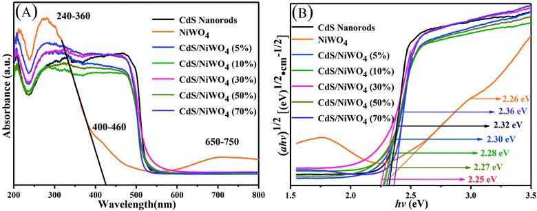
Light absorption performance is of great importance in influencing the H2 production activity. Therefore, we use a diffuse reflectance spectrometer to test the photoresponse behavior of the samples. Fig. 6(A) shows that the pure CdS nanorods have prominent optical absorption in the UV and visible light regions exhibiting an absorption edge located at 525 nm, and that NiWO4 has outstanding optical absorption in the UV and visible light regions. In addition, three absorption bands (240–360 nm, 400–460 nm and 650–750 nm) of NiWO4 can be clearly seen,48 which are caused by the oxidation state of the cations, in agreement with those reported in the literature by M. M. Mohamed and assigned to the NiWO4 formation.48 For [CdS/NiWO4 (x%)] (x = 5, 10, 30, 50, 70), on the one hand, the absorption edge becomes larger, that is to say, their absorption edge has a tendency to red shift;42 on the other hand, the light absorption intensity is enhanced in the wavelength range from 600 to 800 nm.
 |
| | Fig. 6 (A) The UV-vis diffuse reflectance spectra; (B) the plot of transformed Kubelka–Munk function vs. the energy. | |
In order to obtain the energy band gap (Eg) of the samples, we draw the Tauc graph from the UV-vis diffuse reflectance spectra. The Eg is estimated by the function (eqn (2)):
| |  | (2) |
From CdS nanorods to [CdS/NiWO4 (70%)], the Eg values are estimated to be 2.32, 2.26, 2.30, 2.28, 2.27, 2.25 and 2.36 eV, respectively. It may be the different colors of the samples and different percentages of NiWO4 that lead to different light absorption intensities. The light absorption intensity of the photocatalyst increases with the increase of the percentage of NiWO4. Nevertheless, excessive loading of NiWO4 on the surface of CdS nanorods will prevent CdS from absorbing visible light,41 thereby reducing the photocatalytic H2 production activity.
3.3 Photocatalytic H2 evolution performance
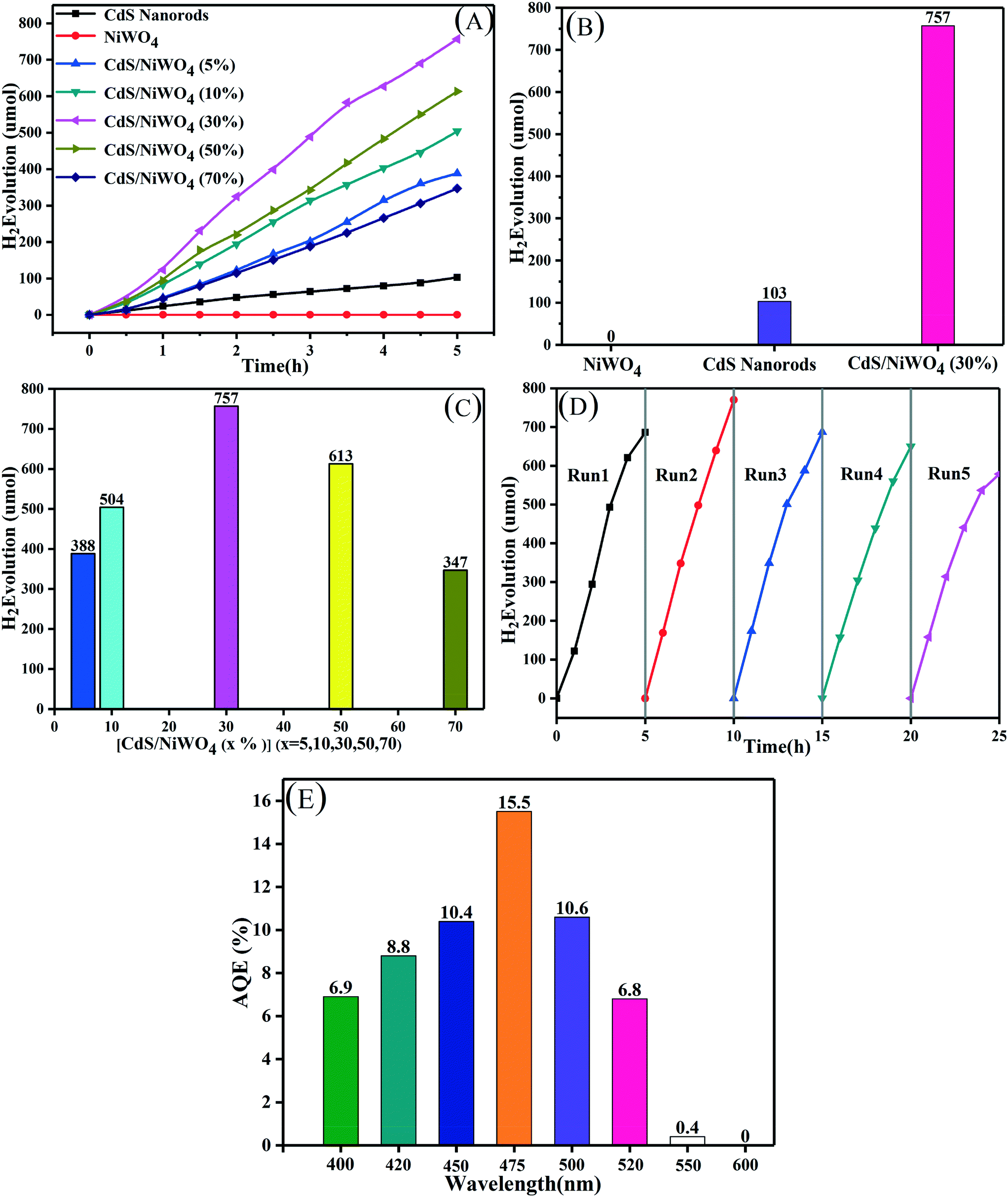
In order to test the photocatalytic H2 production performance and the stability of the samples, they are tested in a 10% lactic acid solution, and the results are shown in Fig. 7. We break down Fig. 7(A) into Fig. 7(B) and (C) so that we can study the H2 production performance of CdS nanorods and NiWO4 and the effect of different percentages of NiWO4 on the H2 production performance. From Fig. 7(B), we can see that pure NiWO4 did not produce H2 within 5 h, which means that pure NiWO4 has no photocatalytic H2 production activity. The H2 production of CdS nanorods for 5 hours is the smallest, reaching 103 μmol, due to the rapid recombination of photogenerated electrons and holes. When 30% NiWO4 is deposited on the surface of CdS nanorods, by testing, the H2 production amount reaches the maximum of 757 μmol, which is 7.35 times higher than that of CdS nanorods.
 |
| | Fig. 7 (A–C) The H2 production activity curves of CdS nanorods, NiWO4 and [CdS/NiWO4 (x%)] (x = 5, 10, 30, 50, 70) in 30 ml 10% lactic acid solution; (D) stability test on the [CdS/NiWO4 (30%)] sample; (E) the AQE of the [CdS/NiWO4 (30%)] sample in 30 ml 10% lactic acid solution. | |
In order to study the effect of the content of NiWO4 on the H2 production activity, we test the H2 production performance of the different percentages of the composite catalyst [CdS/NiWO4 (x%)] (x = 5, 10, 30, 50, 70) prepared above, and the results are shown in Fig. 7(C). The hydrogen yield of the composite catalysts exhibits the shape of an arch bridge, that is, as the percentage content of NiWO4 increases, the amount of H2 production also increases. The amount of H2 production reaches the maximum (757 μmol, 5 h) when the percentage content of NiWO4 is 30%. Subsequently, when the percentage of NiWO4 is continuously increased, the amount of hydrogen production begins to decrease gradually. This may be attributed to the phenomenon that superfluous NiWO4 not only can absorb more visible light by itself, but also can occupy some active sites of CdS nanorods, thus inhibiting the H2 production activity.41
Further, in order to evaluate the stability of catalyst activity, the [CdS/NiWO4 (30%)] sample is selected to be tested in a 10 vol% lactic acid solution. We perform a total of 5 cycles of 5 hours each. When the end of each cycle is ended, the reaction system is replaced with N2 to remove hydrogen from the last cycle. In Fig. 7(D), we can see that the total amount of H2 in each cycle is almost equal and the slight decrease in hydrogen production in the fifth cycle may be due to lactic acid consumption, which indicates that the catalyst activity is relatively stable. Further, we test the AQE of the [CdS/NiWO4 (30%)] composite catalyst at different wavelengths. The results are shown in Fig. 7(E): it can be seen that as the monochromatic wavelength increases, the AQE also increases, and the AQE reaches 15.5% when the monochromatic wavelength is 475 nm. When a larger monochromatic wavelength is used, the AQE begins to decrease; when the monochromatic wavelength is up to 550 nm, the AQE is only 0.4%, indicating that the catalyst produces little H2 at this wavelength. When the wavelength of monochromatic light is 600 nm, the AQE is 0, indicating that the wavelength cannot excite the [CdS/NiWO4 (30%)] composite catalyst.
We can draw conclusions from the above analysis results: the p–n type heterojunction between CdS nanorods and NiWO4 is successfully formed; under the internal electric field and potential difference, the electron and hole migration speeds are accelerated, thus improving the H2 production performance of the composite catalyst.
3.4 Separation mechanism of charge transfer
3.4.1 PL spectra and TRPL spectra.
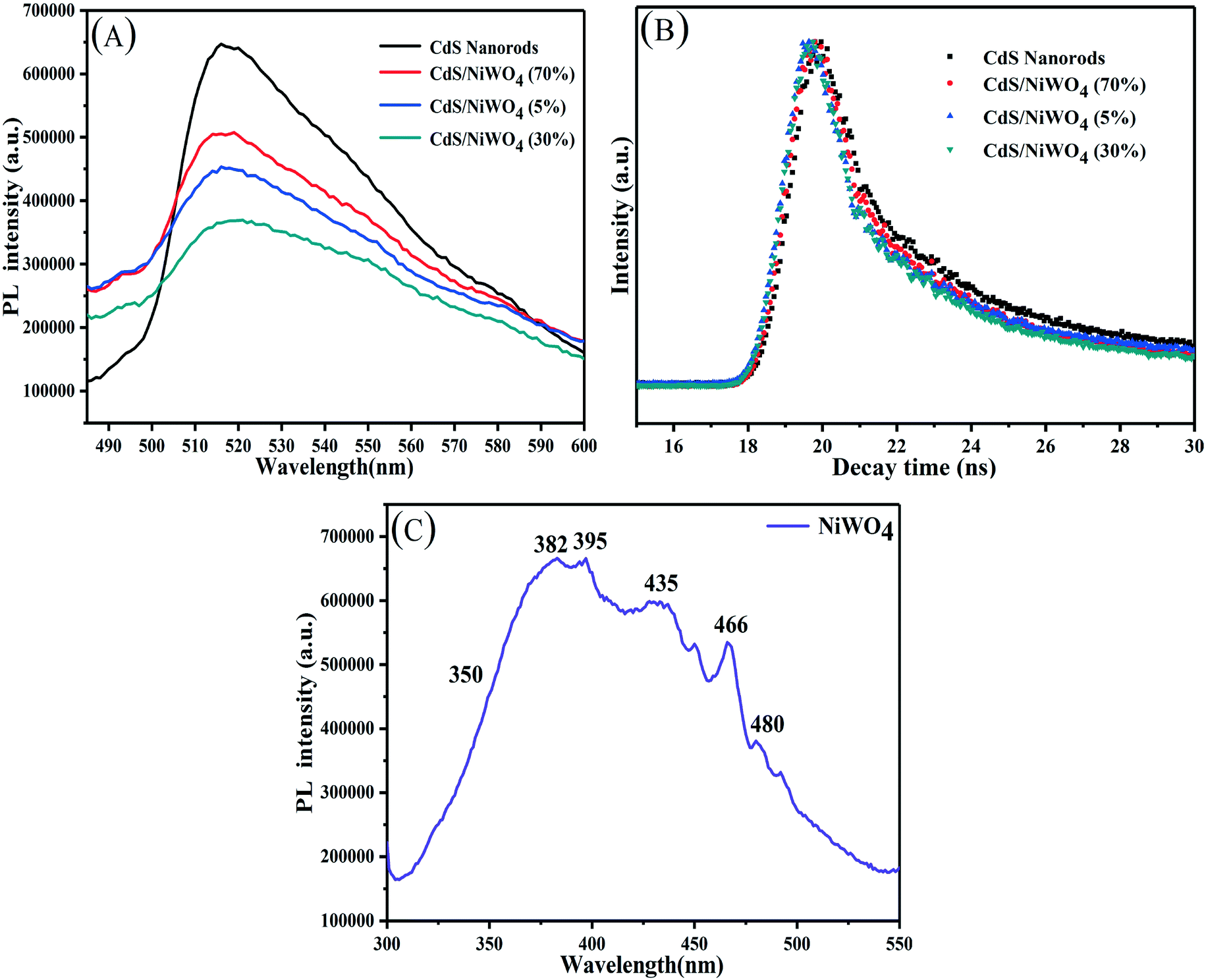
The separation and transfer of charge and the lifetime of electrons and holes are of great importance in elucidating the possible charge separation and transfer mechanisms. Therefore, photoluminescence experiments and fluorescence lifetime decay experiments are carried out. The results are shown in Fig. 8 and Table 2. Fig. 8(A and C) show the photoluminescence (PL) spectra of CdS nanorods, [CdS/NiWO4 (5%)], [CdS/NiWO4 (30%)], [CdS/NiWO4 (70%)] and NiWO4. In Fig. 8(A), the PL spectra of all the samples present a parabolic shape with different intensities. Their emission wavelength center is approximately 520 nm while the excitation wavelength is 380 nm. In Fig. 8(C), when the excitation wavelength is 290 nm, the emission wavelength of NiWO4 nanoparticles ranges from 300 to 550 nm, which is similar to other wolframite compounds.32 It is the WO66− anion along with some defects in the crystal structure that determines the fluorescence emission peak of NiWO4.32 The emission peak at 350 nm is from the band gap transition. The doublet peaks appear at 382 and 395 nm, which are due to either the quantum size49 or to the interference between the luminescence band of the WO6 groups and the absorption band of the NiO6 groups.50 The other obvious emission peaks appear at 435, 466 and 480 nm, which are related to the intensive transition from the ground state 3A2g to the excited state 3T1 of Ni2+ (3d8) ions in a distorted octahedral coordination32 or due to recombination of e–h pairs localized at oxygen-atom-deficient tungstate ions.51 Compared with that of CdS nanorods, the emission peak fluorescence intensity of NiWO4 is the strongest, which indicates that it has the highest degree of combination of electrons and holes. When different amounts of NiWO4 are adhered to the surface of CdS nanorods, the fluorescence intensity of the emission peaks is quenched to varying degrees. As the percentage of NiWO4 increases, the emission peak intensity first decreases and then increases, and the emission peak of [CdS/NiWO4 (30%)] is the weakest and quenched to the maximum extent. Based on the above results, we can further draw the conclusion: the p–n junction and an internal electric field between NiWO4 and CdS are formed. It is the internal electric field that accelerates the rapid separation and transfer of electrons and holes, thereby effectively enhancing the photocatalytic activity of H2 production.
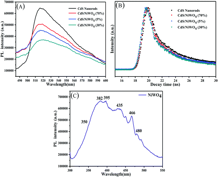 |
| | Fig. 8 (A and C) The PL spectra and (B) the time-resolved photoluminescence (TRPL) spectra. | |
Table 2 The exponential curve fitted parameters of emission decay for the samples
| Samples |
T
1 [ns] |
A
1 [%] |
T
2 [ns] |
A
2 [%] |
T
3 [ns] |
A
3 [%] |
χ
2
|
τ
ave [ns] |
K
ET [109 s−1] |
η
(inj) [%] |
| CdS |
5.60 |
22.11 |
0.69 |
17.58 |
160.4 |
60.31 |
1.89 |
3.96 |
— |
— |
| CdS/NiWO4 (70%) |
5.32 |
22.67 |
0.59 |
17.75 |
150.8 |
59.58 |
1.90 |
2.90 |
0.092 |
26.7 |
| CdS/NiWO4 (5%) |
5.24 |
22.96 |
0.55 |
18.56 |
149.5 |
58.48 |
1.91 |
2.58 |
0.135 |
34.8 |
| CdS/NiWO4 (30%) |
4.44 |
25.90 |
0.41 |
19.54 |
101.7 |
54.65 |
2.02 |
1.87 |
0.282 |
52.7 |
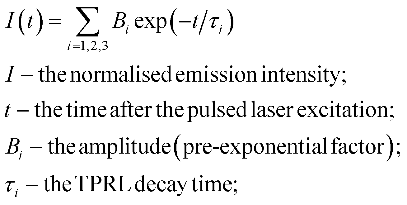
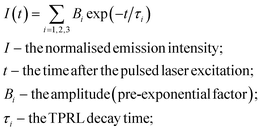
What's more, time-resolved photoluminescence (TRPL) is a promising approach to observe the kinetics of electron transfer and further study the separation and transfer of photogenerated electrons and holes. In Fig. 8(B), the decay curves of the samples are fitted by a triexponential decay function (eqn (3)).27 The composite catalysts demonstrate a faster TRPL decay compared with CdS nanorods, which indicates efficient charge separation.
| |  | (3) |
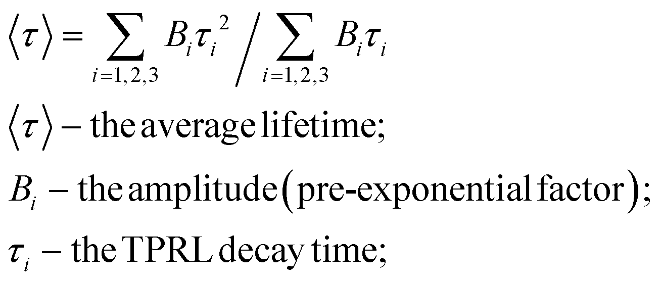
From the fitting parameters in Table 2, it can be seen that the short lifetime (T1, T2) and long lifetime (T3) gradually reduce. We use eqn (4)27 to calculate the average lifetime (τave) so that we can better understand the effect of NiWO4 content on the decay life of the composite catalysts.
| |  | (4) |
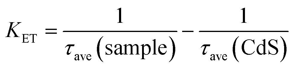
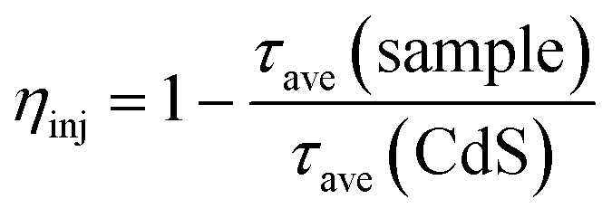
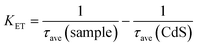
The average lifetime of CdS nanorods, [CdS/NiWO4 (70%)], [CdS/NiWO4 (5%)] and [CdS/NiWO4 (30%)] is 3.96, 2.90, 2.58 and 1.87 ns, respectively. Generally speaking, the shorter the electron lifetime, the faster the electron transfer rate. The above results reflect the transfer of electrons from CdS nanorods to NiWO4 in a relatively short period of time. Using the average lifetime of the samples, we further calculate the electron transfer rate constant (KET)52 and the electron injection efficiency (ηinj)53,54 using eqn (5) and (6) respectively:
| |  | (5) |
| |  | (6) |
Based on the above formula, from [CdS/NiWO4 (5%)] to [CdS/NiWO4 (30%)], the electron transfer rate constant (KET) and electron injection efficiency (ηinj) are calculated to be 0.092 × 10⁹, 0.135 × 10⁹, 0.282 × 10⁹ s−1 and 31.4, 36.9 and 44.7%, respectively. Therefore, the above results further prove that the p–n type heterojunction between NiWO4 and CdS is successfully formed. It's the p–n heterojunction that makes the electrons rapidly transfer from the conduction band (CB) of NiWO4 to that of CdS in a relatively short time, further participating in the process of H2 production.
3.4.2 Photoelectrochemical (i–t and EIS) analysis.
It is well known that the photoelectric properties of catalysts are also important factors affecting the separation and transfer of electrons and holes. Photocurrent density–time experiments (i–t) and AC impedance experiments (EIS) were conducted to determine the photoelectric properties of the samples. To this end, we carry out the above experiments in 0.2 M Na2SO4 aqueous solution.
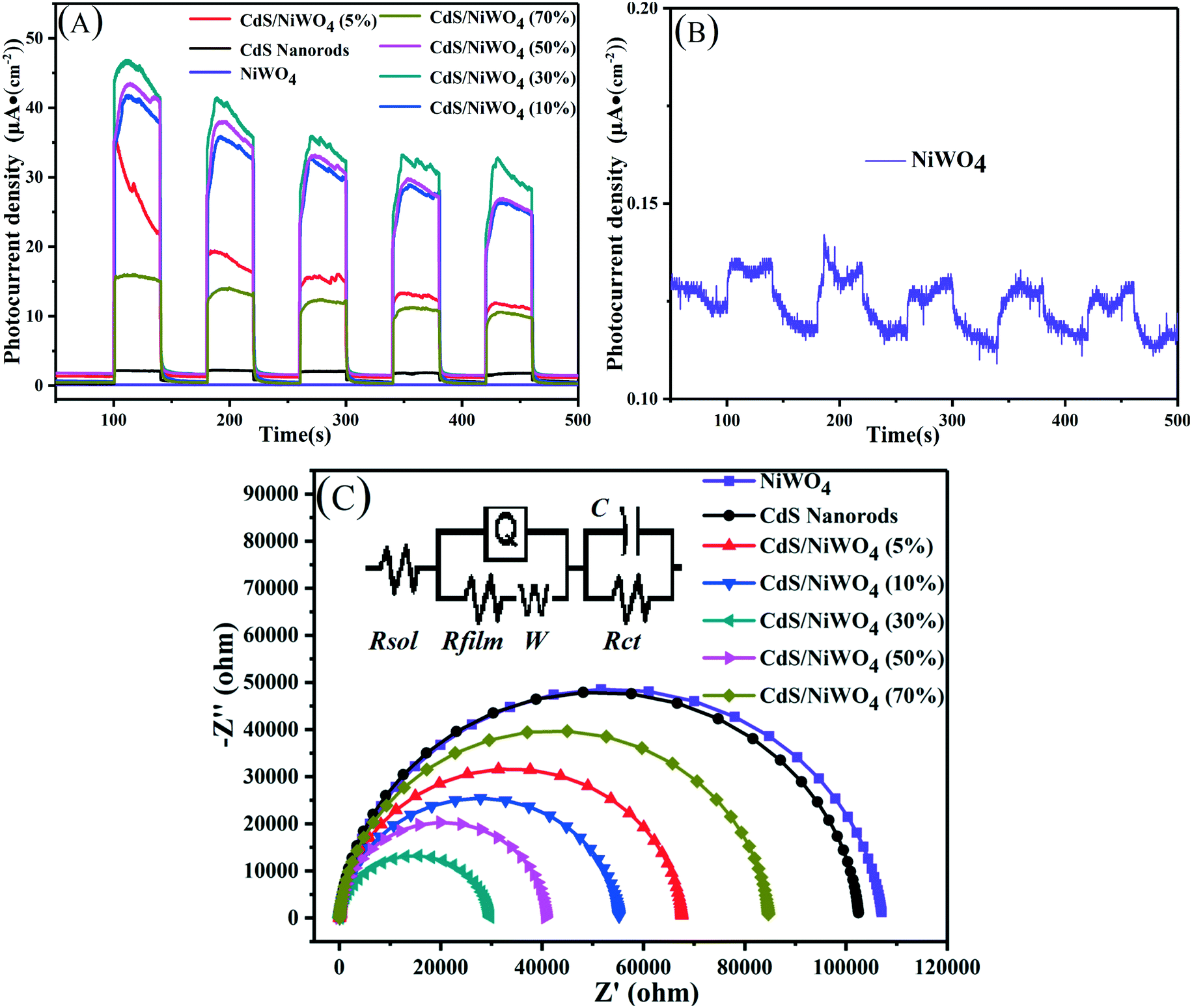
Fig. 9(A) shows the photocurrent density–time curve of CdS nanorods, NiWO4 and [CdS/NiWO4 (x%)] (x = 5, 10, 30, 50, 70). In order to observe the photocurrent response of NiWO4 clearly and intuitively, we deconvolute the photocurrent response of NiWO4 in Fig. 9(A), and the result is shown in Fig. 9(B). It can be seen that NiWO4 nanoparticles have the lowest photocurrent density, and that the photocurrent density of pure CdS nanorods is improved to some extent compared to that of NiWO4 nanoparticles. Further, considering Fig. 9(A and B), it can be concluded that the photocurrent density of the pure CdS nanorods is 16.24 times higher than that of the NiWO4 nanoparticles. When NiWO4 is loaded onto the CdS nanorods, the photocurrent density of the composite catalyst is improved. After 5 cycles of light on/off, the photocurrent density of the composite catalyst showed a downward trend, which may be due to the existence of certain photo-corrosion of CdS under light conditions in 0.2 M Na2SO4 aqueous solution. On further observation, it can be found that with the increase of NiWO4 content, the photocurrent density of the composite catalyst also increases; when the loading of NiWO4 reaches 30%, the photocurrent density is the largest; when the content of NiWO4 continues to increase, the photocurrent density begins to decrease. The photocurrent density results of the above samples correspond to the photocatalytic hydrogen production activity shown in Fig. 7(A).
 |
| | Fig. 9 (A) Transient photocurrent responses; (B) transient photocurrent response of NiWO4; (C) electrochemical impedance spectroscopy (EIS) (0.2 M Na2SO4, λ ≥ 420 nm). | |
The AC impedance spectroscopy (EIS) technique can be used to qualitatively study the migration ability of electrons in a photoanode film and the electron exchange capability between the photoanode and the electrolyte interface. Fig. 9(C) shows the AC impedance spectrum of CdS nanorod, NiWO4 and [CdS/NiWO4 (x%)] (x = 5, 10, 30, 50, 70) photoelectrodes in dark state. The smaller the arc radius, the smaller the interface charge transfer resistance. The arc radius of [CdS/NiWO4 (30%)] is the smallest, which means that the conductivity of the [CdS/NiWO4 (30%)] photoelectrode is outstanding. The illustration shows the equivalent circuit diagram. The solution resistance (Rsol), the transfer resistance of photogenerated electrons in the photoelectrode material (Rfilm) and the interfacial reaction resistance (Rct) together constitute the AC impedance value of the photoelectrode. In addition, Q represents the original phase angle; C represents the interface capacitance. The fitted EIS data of CdS and [CdS/NiWO4 (30%)] are shown in Table 3. It can be seen from the fitting results in Table 3 that the Rfilm of the CdS nanorods modified by NiWO4 decreased from 2.77 × 10⁴ Ω cm2 to 2785 Ω cm2, which is about 10 times lower; the Rct decreased from 11.43 Ω cm2 to 1.74 Ω cm2; C is increased from 9.43 × 10⁻⁵ μF cm−2 to 3.2 × 10⁻³ μF cm−2, indicating that the surface state density of the NiWO4 modified CdS nanorods has increased significantly. The above results indicate that the interface electric field formed between NiWO4 and CdS nanorods enhances the separation of electrons and holes, thereby effectively suppressing charge recombination.
Table 3 The parameters of potentiostatic EIS fitted by ZsimpWin
| Samples |
R
sol [Ω cm2] |
Q [Ω−1 cm2 sn] |
n
|
R
film [Ω cm2] |
W
ss [Ω cm2] |
C [μF cm−2] |
R
ct [Ω cm2] |
| CdS nanorods |
25.86 |
2.36 × 10⁻⁵ |
0.927 |
2.77 × 10⁴ |
1.53 × 10⁻⁵ |
9.43 × 10⁻⁵ |
11.43 |
| CdS/NiWO4 (30%) |
23.99 |
8.24 × 10⁻⁵ |
0.854 |
2785 |
1.01 × 10⁻⁵ |
3.2 × 10⁻³ |
1.74 |
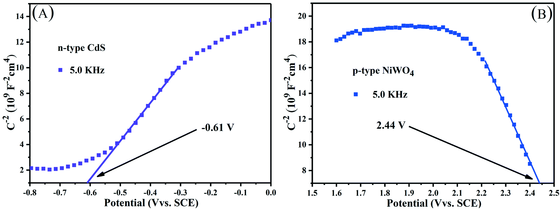
3.5 Potential reaction mechanism
When NiWO4 is combined with CdS nanorods, it will cause the change of the energy level potential, thereby establishing a new interface electric field. The Mott–Schottky method test is based on the function of capacitance and scanning potential. Fig. 10 shows the Mott–Schottky curves of CdS nanorods and NiWO4 photoelectrodes. Their flat band potential can be determined by eqn (7):| |  | (7) |
 |
| | Fig. 10 Mott–Schottky plots of (A) n-type CdS nanorods and (B) p-type NiWO4 at a frequency of 5.0 kHz. | |
Along the linear portion of the Mott–Schottky curves of CdS nanorods and NiWO4, the tangent is extended to the abscissa. We can not only see that the flat-band potential of CdS nanorods and NiWO4 is −0.61 and 2.44 V versus SCE, respectively, but also see that CdS nanorods and NiWO4 are an n-type semiconductor with a positive slope and a p-type semiconductor with a negative slope, respectively.55 Generally speaking, for an n-type semiconductor, the ECB is more negative by about −0.1 or −0.2 V than the Efb; for a p-type semiconductor, the EVB is more positive by approximately 0.1 or 0.2V than the Efb.55,56 Therefore, the ECB of CdS nanorods and EVB of NiWO4 are sketchily calculated to be −0.81 and 2.64 V vs. SCE. Based on the formula: ENHE = ESCE + 0.241, the ECB of CdS nanorods and EVB of NiWO4 are calculated to be −0.569 and 2.881 V vs. NHE.
The p–n heterojunction formed between NiWO4 and CdS nanorods is of great importance in promoting the separation of electrons and holes. The Mulliken electronegativity theory (eqn (8) and (9))36,57 is used to estimate the VB and CB band positions of NiWO4 and CdS nanorods so that we can thoroughly understand the formation of the p-NiWO4/n-CdS heterojunction and the energy band structure.
where
χ is the absolute electronegativity of the semiconductor, which is the geometric mean of the electronegativity of the constituent atoms. The
Eg of NiWO
4 and CdS is given in
Fig. 6(B), and is 2.26 and 2.32 eV, respectively. The
χ values of NiWO
4 and CdS are determined to be 6.301 (
ref. 58) and 5.075 eV,
36 respectively.
Ee is the energy of free electrons on the hydrogen scale (4.5 eV
vs. NHE).
Table 4 lists the calculated band positions according to the above formula and relevant data. Through comparison and analysis, the band positions obtained from the Mott–Schottky plot results are close to the calculated ones in
Table 4.
Table 4 The absolute electronegativity, band gap energy, and valence and conduction band edge potential of CdS and NiWO4
| Semiconductor |
Absolute electronegativity (χ) |
Band energy Eg (eV) |
Valence band EVB (eV) |
Conduction band ECB (eV) |
| CdS (n-type) |
5.075 |
2.32 |
1.74 |
−0.58 |
| NiWO4 (p-type) |
6.301 |
2.26 |
2.93 |
0.67 |
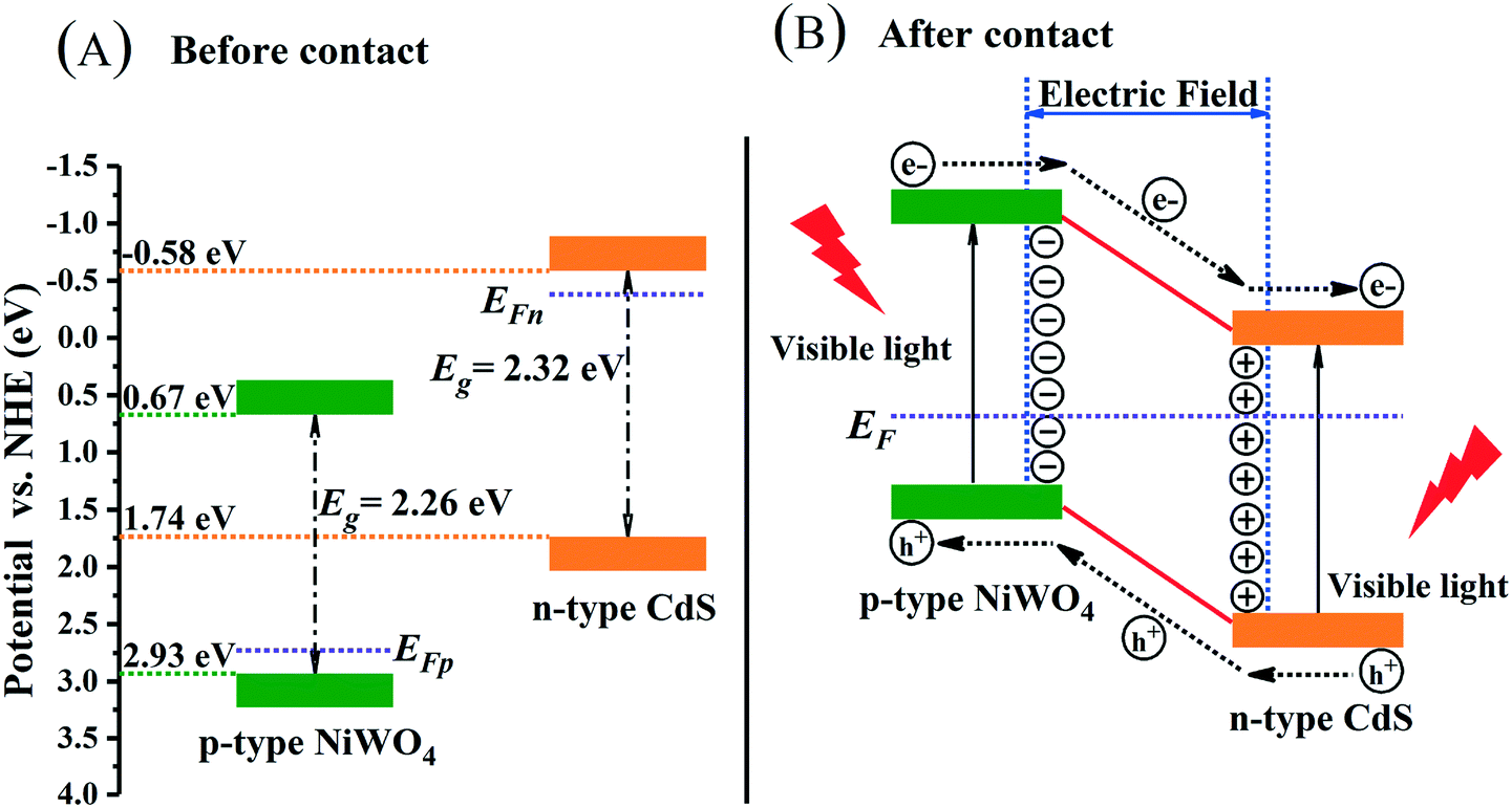
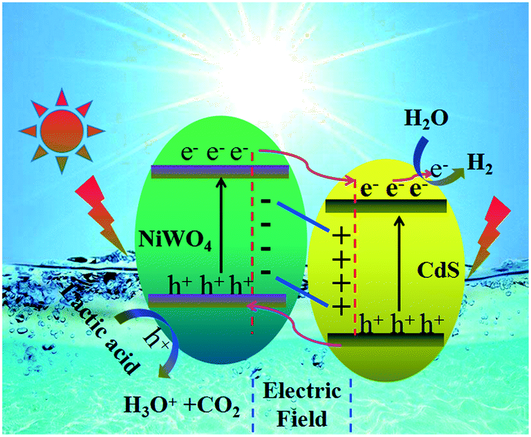
Through the above analysis results, we have drawn the energy band position diagram. Fig. 11 shows the band positions of p-NiWO4 and n-CdS before and after contact. At the same time, Fig. 11 and Scheme 1 describe the charge migration process and the photocatalytic reaction process. As a p-type semiconductor, NiWO4's VB position is more positive and its Fermi level is close to the VB position. However, CdS nanorods are an n-type semiconductor; CdS nanorods' CB position is more negative and its Fermi level is close to the CB position. When NiWO4 is loaded on CdS nanorods, the Fermi level potential of CdS is more negative than the negative potential of NiWO4, which provides a thermodynamic path to promote charge transfer, making the electrons diffuse from the CB of CdS to the CB of NiWO4, resulting in negative charge accumulation in NiWO4. At the same time, holes migrate from the VB of NiWO4 to the VB of CdS nanorods, resulting in the accumulation of positive charges in the CdS nanorods until their Fermi levels are equal. During the Fermi level shifting, the energy bands of the NiWO4 and CdS nanorods move up and down as the Fermi level moves until the two Fermi levels reach equilibrium. Finally, at equilibrium, an internal electric field from the CdS to NiWO4 direction is established at the interface between NiWO4 and CdS nanorods. Under visible light irradiation, CdS and NiWO4 can be excited to generate electrons and holes. Subsequently, under the action of the potential difference and the internal electric field, electrons can be rapidly transferred from the CB of NiWO4 to the CB of the CdS nanorods, and further migrated to the surface of the CdS nanorods to participate in the reduction of protons to produce H2. At the same time, photogenerated holes migrate from the VB of CdS nanorods to the VB of NiWO4, further migrate to the surface of NiWO4, and then oxidize lactic acid to produce CO2 and H3O+, thereby effectively promoting the separation of electrons and holes, and improving the photocatalytic H2 production efficiency of the composite catalyst.
 |
| | Fig. 11 Schematic diagrams for energy bands of p-NiWO4 and n-CdS (A) before contact and (B) after the formation of the p–n heterojunction. | |
 |
| | Scheme 1 Photocatalytic mechanism of the CdS/NiWO4 system. | |
4. Conclusions
In conclusion, a highly-efficient CdS/NiWO4 p–n heterojunction composite catalyst is successfully constructed. In the composite catalyst, the introduction of NiWO4 simultaneously improves the photocatalytic H2 production performance of CdS nanorods and the stability of photocatalytic H2 production. The photocatalytic H2 production properties of the CdS/NiWO4 composite catalyst are closely related to the loading capacity of NiWO4. The [CdS/NiWO4 (30%)] sample has the best H2 production performance. Under visible light irradiation, the maximum H2 production in 5 hours is 757 μmol, which is 7.35 times higher than that of pure CdS nanorods. Further studies of photoluminescence spectra, photoelectrochemistry experimental results and Mott–Schottky curves show that the modification of NiWO4 enhances the electron mobility and charge transfer ability of the composite catalyst. However, excessive NiWO4 will reduce the light absorption intensity of CdS nanorods, thereby reducing the hydrogen production activity. It is the built-in electric field formed between NiWO4 and CdS nanorods that accelerates the separation of photogenerated electrons and holes. At the same time, the photogenerated holes on the VB of CdS nanorods can be quickly transferred to the surface of NiWO4, which slows down the photo-corrosion of CdS.
Author contributions
Yongke Zhang and Zhiliang Jin conceived and designed the experiments; Yongke Zhang performed the experiments; Zhiliang Jin contributed reagents/materials and analysis tools; and Yongke Zhang wrote the paper.
Conflicts of interest
The authors declare that they have no competing interests.
Acknowledgements
This work was financially supported by the Chinese National Natural Science Foundation (21862002 and 41663012), the innovation project (YCX18082), North Minzu University, the new technology and system for clean energy catalytic production, and the major scientific project of North Minzu University (ZDZX201803).
References
- X. P. Tao, Y. Zhao, L. C. Mu, S. Y. Wang, R. G. Li and C. Li, Bismuth Tantalum Oxyhalogen: A Promising Candidate Photocatalyst for Solar Water Splitting, Adv. Energy Mater., 2017, 1701392 Search PubMed.
- J. Low, J. Yu, M. Jaroniec, S. Wageh and A. A. Al-Ghamdi, Heterojunction Photocatalysts, Adv. Mater., 2017, 29, 1601694 CrossRef PubMed.
- X. Q. Hao, Y. C. Wang, J. Zhou, Z. W. Cui, Y. Wang and Z. G. Zou, Zinc vacancy-promoted photocatalytic activity and photostability of ZnS for efficient visible-light-driven hydrogen evolution, Appl. Catal., B, 2018, 221, 302–311 CrossRef CAS.
- X. Hai, W. Zhou, K. Chang, H. Pang, H. M. Liu, L. Shi, F. Ichihara and J. H. Ye, Engineering Crystallinity of MoS2 Monolayers for Highly Efficient Solar Hydrogen Production, J. Mater. Chem. A, 2017, 5, 8591–8598 RSC.
- X. T. Zheng, W. L. Chen, L. Chen, Y. J. Wang, X. W. Guo, J. B. Wang and E. B. Wang, A Strategy for Breaking Polyoxometalate-based MOFs To Obtain High Loading Amounts of Nanosized Polyoxometalate Clusters to Improve the Performance of Dye-sensitized Solar Cells, Chem. – Eur. J., 2017, 23, 8871–8878 CrossRef CAS PubMed.
- H. Wang, X. Lang, R. Hao, L. Guo, J. Li, L. Wang and X. Han, Facet-Defined AgCl Nanocrystals with Surface-Electronic-StructureDominated Photoreactivities, Nano Energy, 2016, 19, 8–16 CrossRef CAS.
- X. Chen, S. Shen, L. Guo and S. S. Mao, Semiconductor-Based Photocatalytic Hydrogen Generation, Chem. Rev., 2010, 110, 6503–6570 CrossRef CAS PubMed.
- Z. C. Guan, H. P. Wang, X. Wang, J. Hu and R. G. Du, Fabrication of heterostructured β-Bi2O3-TiO2 nanotube array composite film for photoelectrochemical cathodic protection applications, Corros. Sci., 2018, 136, 60–69 CrossRef CAS.
- H. Q. Xu, J. Hu, D. Wang, Z. Li, Q. Zhang, Y. Luo, S. H. Yu and H. L. Jiang, Visible-Light Photoreduction of CO2 in a Metal-Organic Framework: Boosting Electron-Hole Separation via Electron Trap States, J. Am. Chem. Soc., 2015, 137, 13440–13443 CrossRef CAS PubMed.
- X. G. Meng, S. X. Ouyang, T. Kako, P. Li, Q. Yu, T. Wang and J. H. Ye, Photocatalytic CO2 conversion over alkali modified TiO2 without loading noble metal cocatalyst, Chem. Commun., 2014, 50, 11517 RSC.
- A. Fujishima and K. Honda, Electrochemical Photolysis of Water at a Semiconductor Electrode, Nature, 1972, 238, 37–38 CrossRef CAS PubMed.
- X. Bai, L. Wang, R. Zong, Y. Lv, Y. Sun and Y. Zhu, Performance Enhancement of ZnO Photocatalyst via Synergic Effect of Surface Oxygen Defect and Graphene Hybridization, Langmuir, 2013, 29, 3097–3105 CrossRef CAS PubMed.
- Q. Li, B. D. Guo, J. G. Yu, J. R. Ran, B. H. Zhang, H. J. Yan and J. R. Gong, Highly Efficient Visible-Light-Driven Photocatalytic Hydrogen Production of CdS-Cluster-Decorated Graphene Nanosheets, J. Am. Chem. Soc., 2011, 133, 10878–10884 CrossRef CAS PubMed.
- X. Wu, H. B. Zhang, J. C. Dong, M. Qiu, J. T. Kong, Y. F. Zhang, Y. Li, G. L. Xu, J. Zhang and J. H. Ye, Surface Step Decoration of Isolated Atom as Electron Pumping: AtomicLevel Insights into Visible-Light Hydrogen Evolution, Nano Energy, 2018, 45, 109–117 CrossRef CAS.
- B. B. Zhang, G. J. Dong, L. Wang, Y. J. Zhang, Y. Ding and Y. P. Bi, Efficient hydrogen production from MIL-53(Fe) catalyst-modified Mo: BiVO4
photoelectrodes, Catal. Sci. Technol., 2017, 7, 4971 RSC.
- G. C. Xi and J. H. Ye, Synthesis of bismuth vanadate nanoplates with exposed {001} facets and enhanced visible-light photocatalytic properties, Chem. Commun., 2010, 46, 1893–1895 RSC.
- Y. P. Bi, H. Y. Hu, S. X. Ouyang, Z. B. Jiao, G. X. Lu and J. H. Ye, Selective Growth of Metallic Ag Nanocrystals on Ag3PO4 Submicro-Cubes for Photocatalytic Applications, Chem. – Eur. J., 2012, 18, 14272 CrossRef CAS PubMed.
- K. Leistner, K. Duschek, J. Zehner, M. Yang, A. Petr, K. Nielsch and K. L. Kavanagh, Role of Hydrogen Evolution during Epitaxial Electrodeposition of Fe on GaAs, J. Electrochem. Soc., 2018, 165(4), H3076–H3079 CrossRef CAS.
- Z. W. Ren, J. K. Sun, H. Li, P. Mao, Y. Z. Wei, X. H. Zhong, J. S. Hu, S. Y. Yang and J. Z. Wang, Bilayer PbS Quantum Dots for High-Performance Photodetectors, Adv. Mater., 2017, 1702055 CrossRef PubMed.
- L. Zhang, H. B. Wu, S. Madhavi, H. H. Hng and X. W. Lou, Formation of Fe2O3 Microboxes with Hierarchical Shell Structures from Metal-Organic Frameworks and Their Lithium Storage Properties, J. Am. Chem. Soc., 2012, 134(42), 17388–17391 CrossRef CAS PubMed.
- B. B. Liu, X. J. Liu, M. Y. Ni, C. J. Feng, X. Lei, C. Li, Y. Y. Gong, L. Y. Niu, J. L. Li and L. K. Pan, SnO2 as co-catalyst for enhanced visible light photocatalytic activity of Bi2MoO6, Appl. Surf. Sci., 2018, 453, 280–287 CrossRef CAS.
- T. P. Hu, P. F. Li, J. F. Zhang, C. H. Liang and K. Dai, Highly efficient direct Z-scheme WO3/CdS-diethylenetriamine photocatalyst and its enhanced photocatalytic H2 evolution under visible light irradiation, Appl. Surf. Sci., 2018, 442, 20–29 CrossRef CAS.
- Q. Y. Li, T. Kako and J. H. Ye, WO3 modified titanate network film: highly efficient photo-mineralization of 2-propanol under visible light irradiation, Chem. Commun., 2010, 46, 5352–5354 RSC.
- M. G. Walter, E. L. Warren, J. R. McKone, S. W. Boettcher, Q. Mi, E. A. Santori and N. S. Lewis, Solar Water Splitting Cells, Chem. Rev., 2010, 110(11), 6446–6473 CrossRef CAS PubMed.
- Y. Y. Bu, Z. Y. Chen, W. B. Li and B. R. Hou, Highly Efficient Photocatalytic Performance of Graphene-ZnO Quasi-ShellCore Composite Material, ACS Appl. Mater. Interfaces, 2013, 5(23), 12361–12368 CrossRef CAS PubMed.
- Z. Zhang and J. T. Yates Jr, Band Bending in Semiconductors: Chemical and Physical Consequences at Surfaces and Interfaces, Chem. Rev., 2012, 112(10), 5520–5551 CrossRef CAS PubMed.
- W. L. Zhen, X. F. Ning, B. J. Yang, Y. Q. Wu, Z. Li and G. X. Lu, The enhancement of CdS photocatalytic activity for water splitting via antiphotocorrosion by coating Ni2P shell and removing nascent formed oxygen with artificial gill, Appl. Catal., B, 2018, 221, 243–257 CrossRef CAS.
- J. Y. Zhang, Y. H. Wang, J. Jin, J. Zhang, Z. Lin, F. Huang and J. G. Yu, Efficient Visible-Light Photocatalytic Hydrogen Evolution and Enhanced Photostability of Core/Shell CdS/g-C3N4 Nanowires, ACS Appl. Mater. Interfaces, 2013, 5, 10317–10324 CrossRef CAS PubMed.
- M. Y. Xing, B. C. Qiu, M. M. Du, Q. H. Zhu, L. Z. Wang and J. L. Zhang, Spatially Separated CdS Shells Exposed with Reduction Surfaces for Enhancing Photocatalytic Hydrogen Evolution, Adv. Funct. Mater., 2017, 27, 1702624 CrossRef.
- M. G. Wang, H. Zhang, H. L. Zu, Z. R. Zhang and J. Han, Construction of TiO2/CdS heterojunction photocatalysts with enhanced visible light activity, Appl. Surf. Sci., 2018, 455, 729–735 CrossRef CAS.
- Q. Liang, S. N. Cui, C. H. Liu, S. Xu, C. Yao and Z. Y. Li, Construction of CdS@UIO-66-NH2 core-shell nanorods for enhanced photocatalytic activity with excellent photostability, J. Colloid Interface Sci., 2018, 524, 379–387 CrossRef CAS PubMed.
- C. Feng, Z. Y. Chen, J. Hou, J. R. Li, X. B. Li, L. K. Xu, M. X. Sun and R. C. Zeng, Effectively enhanced photocatalytic hydrogen production performance of one-pot synthesized MoS2 clusters/CdS nanorod heterojunction material under visible light, Chem. Eng. J., 2018, 345, 404–413 CrossRef CAS.
- Y. J. Zou, J. W. Shi, D. D. Ma, Z. Y. Fan, L. H. Cheng, D. K. Sun, Z. Y. Wang and C. M. Niu, WS2/Graphitic Carbon Nitride Heterojunction Nanosheets Decorated with CdS Quantum Dots for Photocatalytic Hydrogen Production, ChemSusChem, 2018, 11, 1187–1197 CrossRef CAS PubMed.
- D. D. Zheng, G. G. Zhang and X. C. Wang, Integrating CdS quantum dots on hollow graphitic carbon nitride nanospheres for hydrogen evolution photocatalysis, Appl. Catal., B, 2015, 179, 479–488 CrossRef CAS.
- H. M. Wang, C. H. Li, L. Ying and P. F. Fang, WO3&WS2 nanorods coupled with CdS nanoparticles for enhanced visible light driven hydrogen evolution, Appl. Surf. Sci., 2018, 448, 539–546 CrossRef CAS.
- Y. L. Han, Z. B. Liang, H. F. Dang and X. F. Dong, Extremely high photocatalytic H2 evolution of novel Co3O4/Cd0.9Zn0.1S p-n heterojunction photocatalyst under visible light irradiation, J. Taiwan Inst. Chem. Eng., 2018, 1–8 Search PubMed.
- M. M. Mohamed, S. A. Ahmed and K. S. Khairou, Unprecedented high photocatalytic activity of nanocrystalline WO3/NiWO4 hetero-junction towards dye degradation: Effect of template and synthesis conditions, Appl. Catal., B, 2014, 150–151, 63–73 CrossRef CAS.
- M. Pirhashemi and A. H. Yangjeh, ZnO/NiWO4/Ag2CrO4 nanocomposites with p-n-n heterojunctions: highly improved activity for degradations of water contaminants under visible light, Sep. Purif. Technol., 2018, 193, 69–80 CrossRef CAS.
- T. H. Do, C. N. Van, K. A. Tsai, L. T. Quynh, J. W. Chen, Y. C. Lin, Y. C. Chen, W. C. Chou, C. L. Wu, Y. J. Hsu and Y. H. Chu, Superior photoelectrochemical activity of self-assembled NiWO4-WO3 heteroepitaxy, Nano Energy, 2016, 23, 153–160 CrossRef CAS.
- H. Y. Aziz and S. G. Maryam, Novel magnetic Fe3O4/ZnO/NiWO4 nanocomposites: Enhanced visible-light photocatalytic performance through p-n heterojunctions, Sep. Purif. Technol., 2017, 184, 334–346 CrossRef.
- Y. K. Zhang, Z. L. Jin, H. Yuan, G. R. Wang and B. Z. Ma, Well-regulated nickel nanoparticles functional modified ZIF-67(Co) derived Co3O4/CdS p-n heterojunction for efficient photocatalytic hydrogen evolution, Appl. Surf. Sci., 2018, 462, 213–225 CrossRef CAS.
- Y. K. Zhang, G. R. Wang, W. Ma, B. Z. Maa and Z. L. Jin, CdS p-n heterojunction co-boosting with Co3O4 and Ni-MOF-74 for photocatalytic hydrogen evolution, Dalton Trans., 2018, 47, 11176 RSC.
- S. M. Chen, G. Yang, Y. Jia and H. J. Zheng, Three-dimensional NiCo2O4@NiWO4 core-shell nanowire arrays for high performance supercapacitors, J. Mater. Chem. A, 2017, 5, 1028 RSC.
- D. Kumar, S. Hong, D. Reddy and T. Kim, Ultrathin MoS2 layers anchored exfoliated reduced graphene oxide nanosheet hybrid as a highly efficient cocatalyst for CdS nanorods towards enhanced photocatalytic hydrogen production, Appl. Catal., B, 2017, 212, 7–14 CrossRef CAS.
- A. Y. Meng, B. C. Zhu, B. Zhong, L. Y. Zhang and B. Cheng, Direct Z-scheme TiO2/CdS hierarchical photocatalyst for enhanced photocatalytic H2-production activity, Appl. Surf. Sci., 2017, 422, 518–527 CrossRef CAS.
- P. Ye, X. L. Liu, J. Iocozzia, Y. P. Yuan, L. N. Gu, G. S. Xu and Z. Q. Lin, A highly stable non-noble metal Ni2P co-catalyst for increased H2 generation by g-C3N4 under visible light irradiation, J. Mater. Chem. A, 2017, 5, 8493–8498 RSC.
- J. Zhu, W. Z. Li, J. Li, Y. M. Li, H. S. Hu and Y. H. Yang, Photoelectrochemical activity of NiWO4/WO3 heterojunction photoanode under visible light irradiation, Electrochim. Acta, 2013, 112, 191–198 CrossRef CAS.
- M. M. Mohamed, M. Khairy and S. Eid, Polyethylene glycol assisted one-pot hydrothermal synthesis of NiWO4/WO3 heterojunction for direct Methanol fuel cells, Electrochim. Acta, 2018, 263, 286–298 CrossRef CAS.
- A. Kalinko, A. Kotlov, A. Kuzmin, V. Pankratov, A. I. Popov and L. Shirmane, Electronic excitations in ZnWO4 and ZnxNi1-XWO4 (x=0.1-0.9) using VUV synchrotron radiation, Cent. Eur. J. Phys., 2011, 9, 432–437 CrossRef CAS.
- A. L. M. De Oliveira and I. M. G. Dos Santos, Yellow ZnxNi1-xWO4 pigments obtained using a polymeric precursor method, Dyes Pigm., 2008, 77, 210–217 CrossRef CAS.
- Z. D. Lou, J. H. Hao and M. Cocivera, Luminescence of ZnWO4 and CdWO4 thin films prepared by spray pyrolysis, J. Lumin., 2002, 99, 349–453 CrossRef CAS.
- Z. Y. Zhang, J. D. Huang, M. Y. Zhang, Q. Yuan and B. Dong, Ultrathin hexagonal SnS2 nanosheets coupled with g-C3N4 nanosheets as 2D/2D heterojunction photocatalysts toward high photocatalytic activity, Appl. Catal., B, 2015, 163, 298–305 CrossRef CAS.
- X. W. Shi, M. Fujitsuka, S. Kim and T. Majima, Faster Electron Injection and More Active Sites for Efficient Photocatalytic H2 Evolution in g-C3N4/MoS2 Hybrid, Small, 2018, 14, 1703277 CrossRef PubMed.
- S. Q. Peng, X. P. Zeng and Y. X. Li, Titanate nanotube modified with different nickel precursors for enhanced Eosin Y-sensitized photocatalytic hydrogen evolution, Int. J. Hydrogen Energy, 2015, 40, 6038–6049 CrossRef CAS.
- F. Guo, W. Shi, H. Wang, M. Han, H. Li, H. Huang, Y. Liu and Z. Kang, Facile fabrication of a CoO/g-C3N4 p-n heterojunction with enhanced photocatalytic activity and stability for tetracycline degradation under visible light, Catal. Sci. Technol., 2017, 7, 3325–3331 RSC.
- X. Li, J. Yu, J. Low, Y. Fang, J. Xiao and X. Chen, Engineering heterogeneous semiconductors for solar water splitting, J. Mater. Chem. A, 2015, 3, 2485–2534 RSC.
- X. Hao, Z. Jin, H. Yang, G. Lu and Y. Bi, Peculiar synergetic effect of MoS2 quantum dots and graphene on Metal-Organic Frameworks for photocatalytic hydrogen evolution, Appl. Catal., B, 2017, 210, 45–56 CrossRef CAS.
- M. Pirhashemi and A. Habibi-Yangjeh, ZnO/NiWO4/Ag2CrO4 nanocomposites with p-n-n heterojunctions: highly improved activity for degradations of water contaminants under visible light, Sep. Purif. Technol., 2018, 193, 69–80 CrossRef CAS.
|
| This journal is © The Royal Society of Chemistry 2019 |
Click here to see how this site uses Cookies. View our privacy policy here. 
 *abc
*abc