
 Open Access Article
 This Open Access Article is licensed under a
 Creative Commons Attribution 3.0 Unported Licence
Heterogeneous photocatalysts: an overview of classic and modern approaches for optical, electronic, and charge dynamics evaluation
Hui Ling
Tan†
 *a,
Fatwa F.
Abdi
*b and
Yun Hau
Ng
*ac
*a,
Fatwa F.
Abdi
*b and
Yun Hau
Ng
*ac
aParticles and Catalysis Research Group, School of Chemical Engineering, The University of New South Wales, Sydney, NSW 2052, Australia
bHelmholtz-Zentrum Berlin für Materialien und Energie GmbH, Institute for Solar Fuels, Hahn-Meitner-Platz 1, Berlin 14109, Germany. E-mail: fatwa.abdi@helmholtz-berlin.de
cSchool of Energy and Environment, City University of Hong Kong, Hong Kong SAR. E-mail: yunhau.ng@cityu.edu.hk
First published on 14th February 2019
Abstract
The functionality of a photoactive semiconductor (i.e., photocatalysts, photoelectrodes, etc.) is largely dictated by three key aspects: (i) band gap; (ii) absolute potentials of the conduction band minimum and the valence band maximum; and (iii) bulk and surface charge carrier dynamics. Their relevance to governing the energetics and the photo(electro)chemical mechanisms of the semiconductor has prompted development of a multitude of characterization tools to probe the specific characteristic of the material. This review aims to summarize the current experimental techniques, including the conventional and the state-of-the-art tools, directed at examining the key aspects (i), (ii), and (iii) of semiconductors. Although not being exhaustive, this didactic review can be useful to apprise the research community of the sophisticated research tools currently available for characterization of photo(electro)catalyst semiconductors as well as to bridge the multidisciplinary knowledge.
 Hui Ling Tan | Hui Ling Tan received her Bachelor of Engineering degree in Chemical Engineering and PhD degree in Chemical Engineering from the University of New South Wales (UNSW) in 2012 and 2017, respectively. She was a postdoctoral research associate in the School of Chemical Engineering, UNSW. She is now in the Department of Applied Chemistry, Faculty of Engineering at Kyushu University as a Japan Society for the Promotion of Science (JSPS) Postdoctoral Fellow. Her research interests primarily focus on the design and fabrication of metal oxide and carbon-based materials for solar energy conversion applications. |
 Fatwa F. Abdi | Fatwa Abdi is a senior scientist and a group leader at the Institute for Solar Fuels, Helmholtz-Zentrum Berlin (HZB). He obtained his bachelor degree in 2005 from Nanyang Technological University and master's degree in 2006 from National University of Singapore and Massachusetts Institute of Technology, all in Materials Science and Engineering. After a short stint in the semiconductor industry, he pursued a PhD at TU Delft, the Netherlands, and graduated cum laude in 2013. He was the recipient of the Singapore-MIT Alliance fellowship (2005) and Martinus van Marum prize (2014) from the Royal Dutch Society of Sciences and Humanities. His research focuses on the development of solar energy conversion materials and devices. |
 Yun Hau Ng | Yun Hau Ng received his PhD from Osaka University, Japan, in 2009. After a brief research visit to the Radiation Laboratory at the University of Notre Dame (USA), he joined the ARC Centre of Excellence for Functional Nanomaterials at the UNSW with the Australian Postdoctoral Fellowship (APD). He became a lecturer (2014) and senior lecturer (2016) at the School of Chemical Engineering, UNSW. He is currently an associate professor at the School of Energy and Environment, City University of Hong Kong. His research is focused on the development of novel photoactive semiconductors for sunlight energy conversion. He received the Honda–Fujishima Prize in 2013 and the Distinguished Lectureship Award from the Chemical Society of Japan in 2018. |
Key learning points(1) An understanding of the fundamental and key properties (i.e., band gap, band edge positions, and bulk and surface charge carrier dynamics) that dictate the functionality of a semiconductor photo(electro)catalyst.(2) Bridging of multidisciplinary knowledge on different experimental tools currently available for comprehensive studies on the optical, electronic, and charge properties of a semiconductor. (3) Providing “one-stop-shop” for the various experimental techniques, including the standard and the state-of-the-art research tools, available for in-depth examination of the discrete key properties of a semiconductor. (4) An understanding of the inherent limitations of a wide variety of spectroscopic, (photo)electrochemical, time-resolved, and frequency-resolved measurements. (5) Recognizing the emerging in situ/operando measurement techniques for characterizing a semiconductor. |
1. Introduction
The yearning for clean, sustainable, and renewable energy as well as environmental remediation has instigated tremendous research interest in photo(electro)catalysis, which is a robust process for harvesting sunlight as the primary energy source. The burgeoning fields of photo(electro)catalysis include water splitting for H2 generation, CO2 reduction into organic fuels, and organic degradation for environmental pollutant abatement. An appropriate semiconductor, be it organic or inorganic material, is simply needed to bring about the desirable photo(electro)chemical reaction. Apart from being cost-effective and environmentally benign, the practicability of a semiconductor for targeted applications mostly relies on the solar energy conversion efficiency of the material. Recent advancement in photo(electro)catalysis mainly places emphasis on the strategies to enhance light absorption, suppress charge recombination, and improve the charge utilization of the semiconductor so that the solar energy conversion efficiency is optimized. These emergent approaches include semiconductor modification via doping, metal/co-catalyst loading, composite structure, defect induction, crystal facet engineering, and morphological control.1Fundamentally, the overall efficiency of a semiconductor is dictated by three key intrinsic characteristics of the material: (i) energy difference between the conduction band minimum (ECB) and the valence band maximum (EVB), that is, the band gap (Eg); (ii) absolute potentials of the ECB and EVB (i.e., the band position); and (iii) dynamics of the photogenerated electrons and holes such as diffusion length, mobility, and lifetime as well as the rates of surface charge recombination and interfacial charge transfer. These aspects are schematically depicted in Fig. 1. The Eg limits the portion of the solar spectrum that can be utilized to activate the semiconductor (i.e., semiconductors with Eg > 3.0 eV are only responsive toward ultraviolet light, whereas those with smaller band gaps are favorable for more proficient solar energy harvesting). The ECB and EVB potentials define the respective reductive and oxidative powers of the electrons and holes generated upon photoexcitation of the semiconductor. From the thermodynamic point of view, the ECB has to be higher (more negative) than the reduction potential of A/A− to enable reduction of the electron acceptor, whereas the EVB needs to be lower (more positive) than the oxidation potential of D+/D to drive the oxidation of the electron donor. The dynamics of the photoinduced electrons and holes are equally important as they determine the number and efficiency of the charge carriers remaining active to partake in the interfacial reactions at the semiconductor/solution phase boundary in competition with charge recombination.
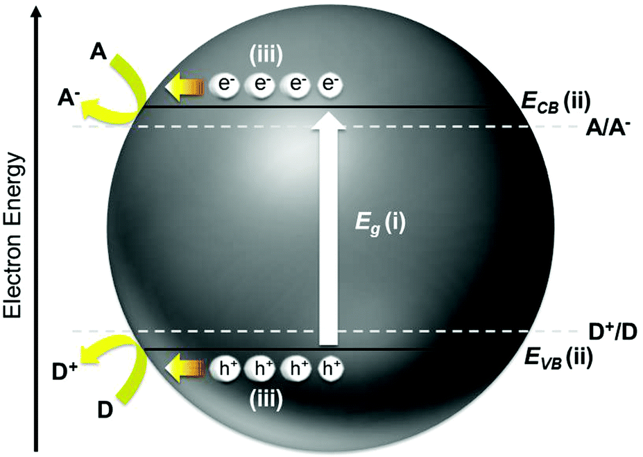 | ||
| Fig. 1 The key aspects that govern the photo(electro)chemical efficiency of a semiconductor photocatalyst. | ||
Determining all the aforementioned aspects is therefore of paramount importance; this will allow us to comprehend the charge energetics, to predict and understand the basic photo(electro)chemical mechanisms, and to exploit the full potential of a semiconductor, particularly for the development of new photo(electro)catalysts. However, in many studies, these properties (i.e., Eg, ECB and EVB levels, and the charge carrier dynamics of the semiconductor) are often obtained from theoretical prediction or by simply adopting values from the literature rather than being directly evaluated experimentally. This may lead to erroneous results, since these properties are known to depend on the specific material composition and/or surface structure.
With the interdisciplinary nature of the photo(electro)catalysis field, numerous characterization methods, particularly those with high sensitivity, selectivity, spatial, temporal, and spectral resolutions, have been greatly developed in the past few decades targeting at the photochemistry, physical chemistry, surface science, and materials science of semiconductor photocatalysts. These methods have been described in the literature, but reports are segregated and usually incomprehensive. This review aims to recapitulate standard and state-of-the-art characterization approaches, although non-exhaustive, for experimental determination of the discrete key properties (i)–(iii) of a semiconductor photo(electro)catalyst. Sections 2 and 3 of this paper cover the determination techniques for Eg and band edge positions, respectively. A brief account of the electronic properties of a semiconductor in the bulk, and at the surface and interface is incorporated in Section 3 to facilitate an understanding of their relevance in ECB and EVB analyses. Section 4 discusses the methods associated with the measurement of charge carrier dynamics both in the bulk and at the semiconductor surface. Finally, the development of combinatorial/in situ characterization techniques to overcome the limitations of the instrumental techniques reviewed in Sections 2–4 is also presented in Section 5.
2. Band gap
Given that the Eg of a semiconductor photo(electro)catalyst fundamentally determines the light absorption ability and the resulting solar conversion efficiency of the material, Eg evaluation is indispensable in the design and development of photo(electro)catalysts. While there are various methods to attain the Eg value of a semiconductor, including electrical conductivity, Hall constant, and photoconductivity measurements, optical methods are by far the most widely employed techniques. Unlike the dependence of electrical conductivity and Hall constant analyses on temperature variation and the uncertainties of photoconductivity associated with surface states, characterization using optical spectroscopies is facile and straightforward to probe the electronic transitions of a solid based on the observed optical absorption or luminescence.Of the manifold optical spectroscopic techniques, ultraviolet-visible (UV-vis) diffuse reflectance spectroscopy is the most frequently used, particularly for thin films and powdered materials. Typically, optical excitation of valence band electrons to the conduction band contributes to an abrupt increase in absorbance at a given wavelength corresponding to the Eg of the semiconductor. An investigation of the tail of the absorption curve of a semiconductor revealed that it exhibits a simple exponential drop. The onset of this drop (which is also the onset of the linear increase in absorption; point A in Fig. 2) has thereafter been identified as the absorption edge. Fochs estimated the Eg of various powdered semiconductors via the onset of the linear increase in diffuse reflectance (R), denoted as point B in Fig. 2. On the other hand, Shapiro determined Eg as the point of intersection between the line extrapolating the linear portion of the absorption curve and the wavelength axis (point C in Fig. 2). These two approaches, however, were argued by Tandon and Gupta to not reflect the onset of the absorption edge as accurate as that of using the point at which the linear increase in absorption starts (i.e., point A).2
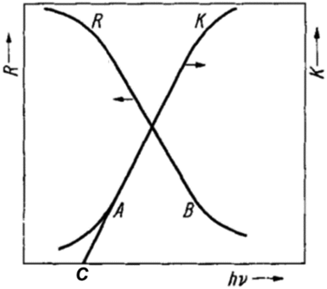 | ||
| Fig. 2 Illustration of different onsets/points in diffuse reflectance (R) and absorption (K) spectra that are employed for Eg determination. Reproduced from ref. 2 with permission from WILEY-VCH Verlag GmbH & Co. KGaA, Weinheim, copyright 1970. | ||
In addition to the conventional graphic representations (i.e., plot of reflectance or absorbance against wavelength) discussed above, numerous empirical relations have also been derived to model the optical absorption edge of semiconductors that result in a range of equations being utilized for the graphical analysis of Eg in the literature. The most common expression being used to date is the one proposed by Tauc, Davis and Mott:3,4
| (αhν)1/n = A(hν − Eg) | (1) |
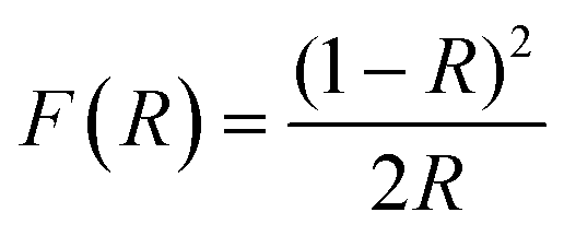 | (2) |
As a result, one of the most general forms of the Tauc plot is with (F(R)hν)1/n as the vertical axis and hν as the horizontal axis. It should be noted that the Eg value obtained via UV-vis spectral analysis strongly depends on the optical electronic transition, the equation used for the graphic representation, and the extrapolation method.
Another optical tool that naturally complements UV-vis diffuse reflectance spectroscopy is the surface photovoltage spectroscopy (SPS). SPS measurements rely on the surface potential changes as a function of the incident photon energy. In principle, redistribution of the excess free carriers generated in a photoexcited semiconductor triggers the surface photovoltage (SPV) signal. Fig. 3a shows the schematic of a typical SPS setup. In short, a metallic box, which serves as a Faraday cage with a dark environment, houses the sample and the probe electrode (e.g., a Kelvin probe or an AFM/STM tip), which are separated at a small distance. The contact potential difference (CPD) between the sample and the probe is then measured, and the change of CPD (ΔCPD) upon illumination is the SPV signal. On the basis of a significant increase in the absorption coefficient near the Eg of most semiconductors with the concomitant substantial change in the SPV signal, the Eg of semiconductors can be estimated simply by identifying the knee (i.e., local maximum) in the SPV curve.6,7 Examples for the application of this approach are displayed in Fig. 3b and c, in which sharp changes in the slopes of the SPV curves were used to determine the Eg of GaAs and InP. The major limitation of the Eg analyzed using the SPS technique, however, is that it serves only as an approximation due to the relatively broad onset of the SPV signal. This is attributed to the Franz–Keldysh effect and excitation of trapped states (i.e., defect-state-to-band transition) via sub-band gap illumination.6,7
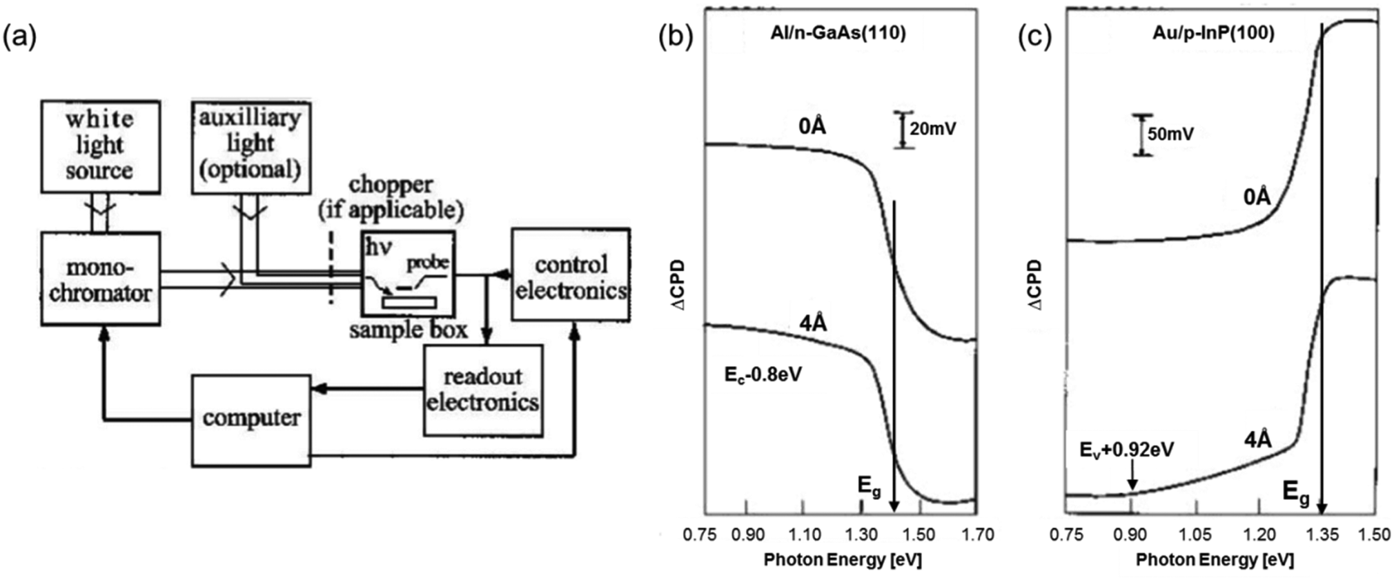 | ||
| Fig. 3 (a) Schematic of a standard SPS configuration. SPS spectra of (b) n-type GaAs (110) surface and (c) p-type InP (100) surface; the top and bottom curves represent the UHV cleaved surface and the surface with an overlayer of Al or Au, respectively. (a and b) Reproduced from ref. 6 with permission from John Wiley & Sons, Ltd, copyright 2001. | ||
Following photoexcitation, the excited electrons would take numerous decay pathways, one being radiative recombination accompanied by photon emission, to return to the ground states. This phenomenon is known as photoluminescence (PL). Steady-state PL spectroscopy has thus also been loosely used to define the Eg of semiconductors. The generic configuration of a photoluminescence setup is illustrated in Fig. 4, in which the three primary components are the excitation light source, the sample cell chamber, and the emitted photon detector. Measurement of the emission spectrum of a sample while it is excited by a monochromatic laser of wavelength energy higher than Eg surveys the permissible electronic transitions from the excited state to the ground state in the material. Proper analysis of the PL spectral distribution therefore enables Eg determination of semiconductors. In spite of that, there are a few key downsides in PL analysis: (1) the necessity to cool the sample to low temperatures (e.g., 77 K or even 4 K) to minimize the competitive non-radiative decay mechanisms that are prevalent at room or higher temperature, thus intensifying the band gap PL emission signal and allowing exploration of the intrinsic optical and electronic properties of the semiconductor;8 (2) the presence of Stokes shift, in which the emission energy is generally lower than that of the absorption (the excitation energy) due to the energy loss associated with the vibrational relaxation process as explained in the Perrin–Jablonski diagram, impeding accurate Eg determination.
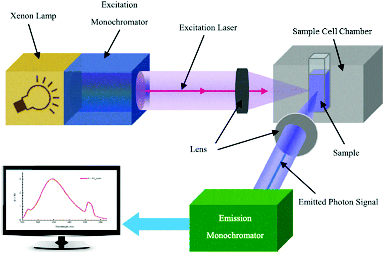 | ||
| Fig. 4 Schematic diagram of the arrangement of optical components in a typical spectrofluorometer. Reproduced from ref. 9 with permission from the IOP Publishing Ltd, copyright 2014. | ||
3. Conduction and valence band edge positions
The (electro)catalytic ability of a semiconductor photocatalyst primarily relies on the electron injection ability of the material at the surface, which is governed by the energetics of the conduction and valence bands. Knowledge on the absolute positions of ECB and EVB band edges is therefore essential to explore the potential applications of the semiconductor of interest. While theoretical calculations based on atomic electronegativities and density functional theory have been demonstrated to be useful to predict the band edge positions for various semiconductors, reliable experimental approaches are crucial and highly sought after. These approaches are discussed in this section. A brief summary of the core energy levels in semiconductors, including Fermi levels, quasi-Fermi levels, vacuum levels, and flatband potentials will first be provided due to their relevance to the determination of ECB and EVB potentials.The electrochemical potential of electrons in a semiconductor is determined by the Fermi level (EF). In other words, EF defines the occupation of the energy levels at thermodynamic equilibrium. Statistically, EF is the energy level at which the probability to be occupied by an electron is 0.5. Given the typical electron distribution in a semiconductor, EF lies within the band gap where its position is dependent on the doping concentration and dopant type. For example, the EF of an n-type semiconductor with electrons as the majority carrier lies close to the conduction band (Fig. 5a). For a p-type semiconductor with holes as the majority carrier, on the other hand, the EF locates just above the valence band (Fig. 5b). However, the thermodynamic equilibrium of a semiconductor is perturbed under illumination or external applied bias where excess electrons and holes are photogenerated or injected. The non-equilibrium densities of holes in the valence band and electrons in the conduction band are then described by the quasi-Fermi levels. Typically, the quasi-Fermi level for the majority carriers approximates to the equilibrium EF due to the insignificant increase of the majority carrier density (i.e., n + Δn ≃ n). Meanwhile, due to the small amount of the minority carriers at equilibrium, it can be greatly escalated (i.e., p + Δp ≃ Δp) which results in a shift of its quasi-Fermi level.10,11 In other words, EF acquisition for n-type semiconductors often translates into the determination of the position of the quasi-Fermi level of electrons, whereas it is the quasi-Fermi level of holes for p-type semiconductors. The quasi-Fermi level of the minority carriers can also be estimated, since it is typically assumed that Δn = Δp. For generalization, the technically correct majority carrier quasi-Fermi level will be referred to as EF hereafter. Based on the above considerations, determination of EF corresponds to the conduction band edge position (ECB) for n-type semiconductors (the difference between the two is dependent on the dopant concentration, but it is typically very small for highly doped semiconductors), and it relates to the valence band edge potential (EVB) for p-type semiconductors.
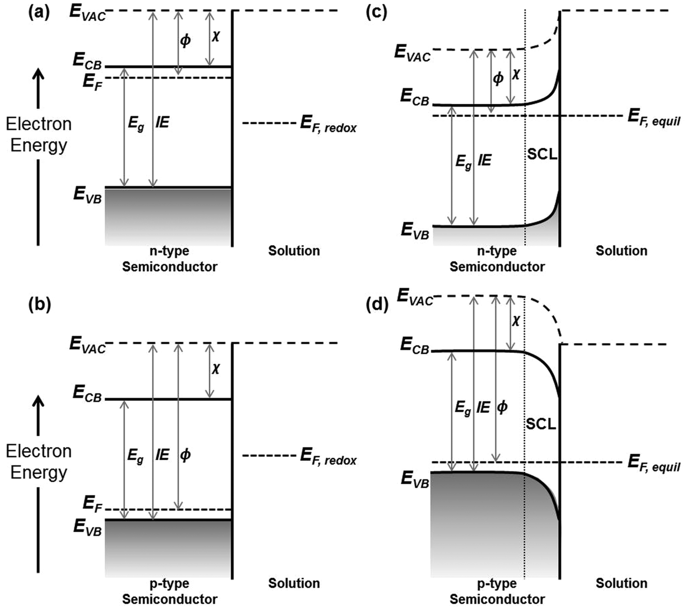 | ||
| Fig. 5 Energy levels of the semiconductor/electrolyte interface (a and b) before and (c and d) after contact. The semiconductors in (a and c) correspond to an n-type semiconductor, whereas (b and d) relate to a p-type semiconductor. EVAC: vacuum level, ECB: bottom of the conduction band, EF: Fermi level, EVB: top of the valence band, Eg: band gap, IE: ionization energy, ϕ: work function, χ: electron affinity. | ||
At the surface, the energy of a stationary electron located in close proximity to the semiconductor relates to the vacuum level (EVAC). As a surface property, EVAC is strongly affected by the surface composition or structure. Nevertheless, it has to be differentiated from the vacuum level at infinity (EVAC(∞)), which is defined as the energy of an electron at rest at an infinite distance from the surface. The disparity between EVAC and EVAC(∞) has been provided by Cahen et al.12 As opposed to EVAC that is accessible experimentally, EVAC(∞) has only theoretical implication and therefore is not considered in this review. Instead, EVAC is the pivotal reference level that defines all the other parameters as illustrated in Fig. 5; the energy needed to excite an electron from EVB, EF, or ECB to EVAC is respectively known as the ionization energy (IE), the work function (ϕ), or the electron affinity (χ). Similar to that of EVAC, all these parameters are surface-related and hence are being defined only at the semiconductor surface.
When a semiconductor is in contact with another phase, the ionic interactions at the interface of the two phases lead to electrostatic adjustments within the material. At the semiconductor/electrolyte interface, in particular, electrons flow from the phase of more negative EF to the other to attain equilibrium, in which the semiconductor EF matches the electrolyte EF,redox. This causes the formation of a space charge layer (SCL) within the semiconductor phase that is associated with the upward bending of the band edges in the n-type semiconductor (Fig. 5c) and downward band bending in the p-type semiconductor (Fig. 5d). The SCL contributes to an internal electric field in the semiconductor, in which the majority carriers are forced away from the semiconductor/electrolyte interface. Such a SCL accounts for one of the three distinct double layers, in addition to the Helmholtz layer and Gouy–Chapman layer that are typically present at the semiconductor/electrolyte interface.10 The magnitude and direction of band bending can simply be adjusted by an externally applied potential. Another important concept to be introduced is the flatband potential (EFB), which is the applied bias that diminishes the band bending in a semiconductor that is in contact with the electrolyte. The EFB therefore carries fundamental significance as it corresponds to the EF of the semiconductor.
Note that the preceding discussion mainly refers to ideal behavior of semiconductors in the absence of surface states for simple presentation of the fundamental and theoretical energetics at the semiconductor/electrolyte interface. The non-ideal behavior of semiconductors can be found elsewhere.10,11
One commonly employed experimental technique to determine band edge positions based on EFB measurement is via (photo)electrochemical methods described as follows:
(1) Capacitance measurement according to the Mott–Schottky function:
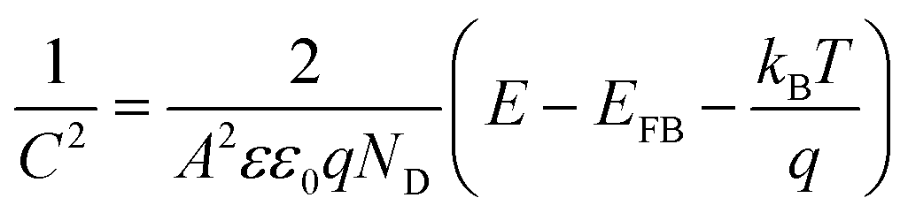 | (3) |
(2) Photocurrent onset examination, in which the EF of the semiconductor is altered using an externally applied potential to show the photocurrent dependence on the potential. The potential value at which the photocurrent appears or vanishes (depending on the potential sweeping direction) corresponds to the EFB of the semiconductor;
(3) Open-circuit photovoltage measurement, in which the electrode open-circuit potential is measured as a function of the illumination intensity. At satisfactorily high intensity, the open-circuit potential becomes constant and can be taken as the EFB of the semiconductor.
A comprehensive discussion on each of these electrochemical-related approaches can be found in the review provided by Beranek.11 Although the review mainly reports the use of the (photo)electrochemical methods on n-type TiO2, they can also be effectually implemented for examination of the EFB for other semiconductors, including p-type materials. However, it must be noted that the obtained results correspond to the ECB for an n-type semiconductor, while it is the EVB for a p-type semiconductor. When one of the band edge potentials is defined, the other can be reasonably deduced based on the Eg value (i.e., Eg = EVB − ECB) analyzed via the methods delineated in Section 2.
In addition to the aforementioned (photo)electrochemical methods, the EFB of semiconductors, particularly in the particle form, can also be effectively acquired by exploiting the equilibrium concentration of an appropriate redox couple (Red/Ox; e.g., MV2+/MV+, Cu2+/Cu+, or C60/C60˙−) upon charge equilibration with the semiconductor.13,14 One example for such a phenomenon is schematically illustrated in Fig. 6. In the presence of the MV+ species that have a redox potential more negative than the semiconductor EF, MV+ is favorably oxidized to form MV2+ (MV+ → MV2+ + e−), and the resulting electrons are then injected into the conduction band of the semiconductor. The electron injection can either raise the Fermi level of the semiconductor to approach the ECB (Fig. 6a) or develop a SCL on the semiconductor surface associated with band bending (Fig. 6b), leading to equilibration between the EF of the semiconductor and the redox potential of the redox couple. This equilibrium potential is therefore identified as the EFB of the semiconductor, which can be calculated according to the Nernst equation:13
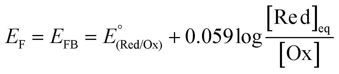 | (4) |
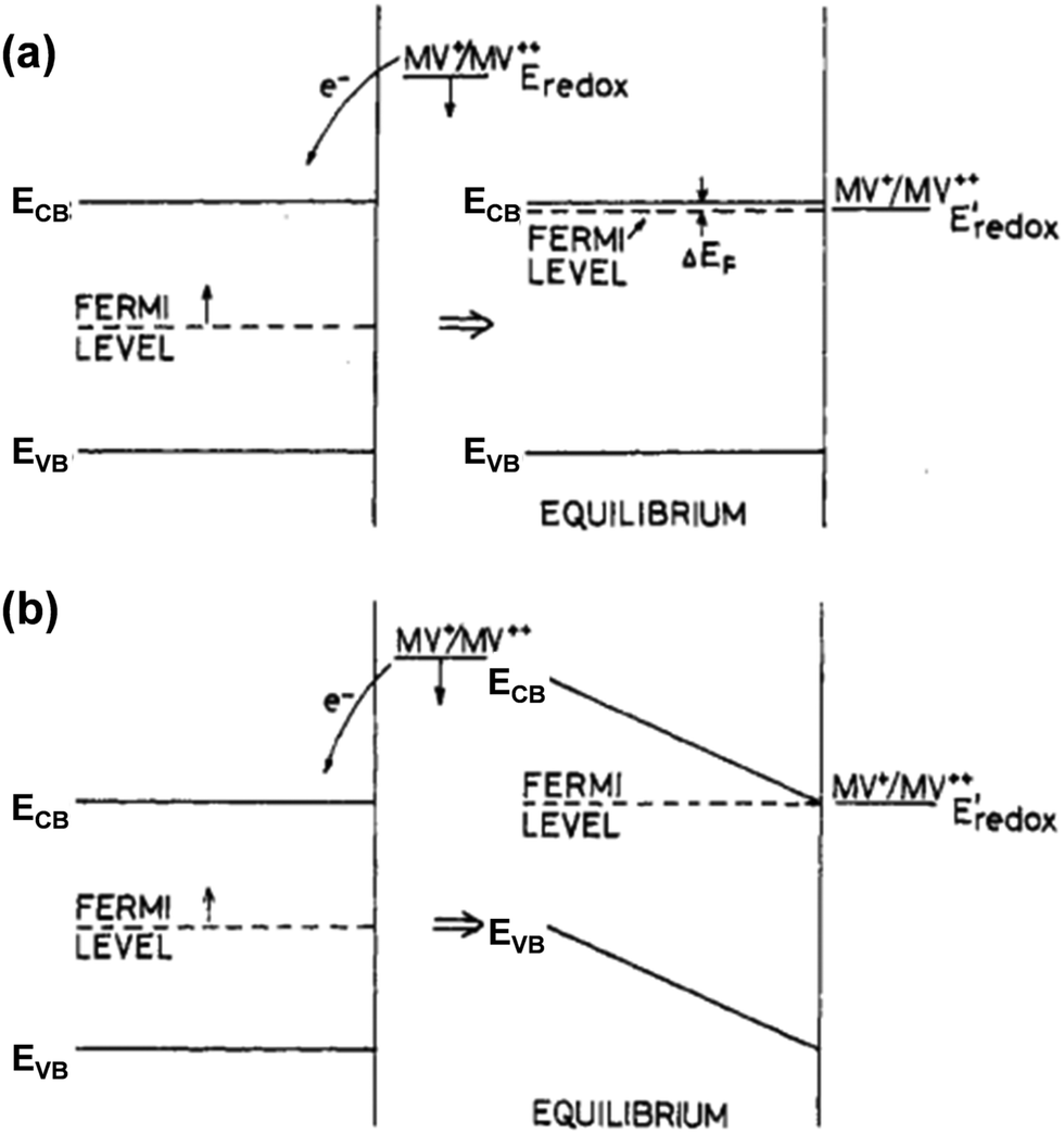 | ||
| Fig. 6 Energy level diagrams of a semiconductor before and after charge equilibration with the MV2+/MV+ redox couple, in which the semiconductor's Fermi level (EF) is more positive than the redox potential of MV2+/MV+. The electron injection from MV2+/MV+ into the semiconductor leads to downward shifting of Eredox to more positive values; meanwhile (a) EF could be shifted upwards such that it approaches ECB or (b) SCL could be formed on the semiconductor surface due to the band bending. In both cases (a and b), Eredox = EF at equilibrium. Reproduced from ref. 14 with permission from the American Chemical Society, copyright 1984. | ||
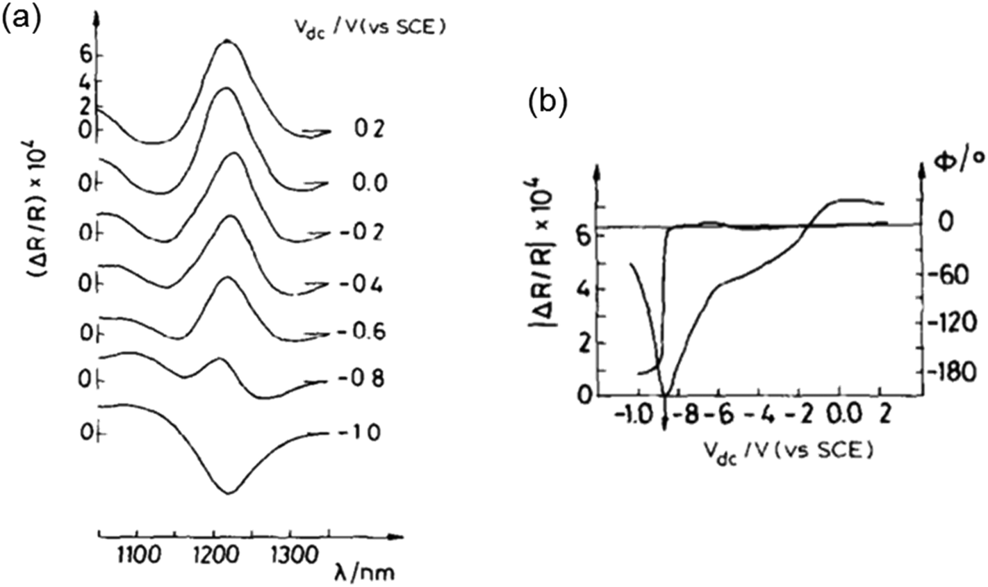 | ||
| Fig. 7 (a) EER spectra of CuInSe2 at different applied Vdc biases. (b) Dependence of the EER signal phase (ϕ) and amplitude (|ΔR/R|) on the applied bias Vdc, measured at λ = 1220 nm. Figure a and b: reproduced from ref. 15 with permission from Elsevier B.V., copyright 1988. | ||
Instead of measuring EF or EFB, the EVB of semiconductors can be directly measured using spectroscopic techniques such as X-ray photoelectron spectroscopy (XPS) and ultraviolet photoelectron spectroscopy (UPS). Typically, the EVB is related to the leading edge (close to 0 eV binding energy) of the photoemission spectra. There are two methods reported to evaluate the EVB value from the XPS valence band spectrum:
(1) Kraut method, a hybrid experimental–theoretical approach, in which the leading edge of the XPS spectrum is modelled and fitted by a Gaussian broadened theoretical valence band density of states;16
(2) Linear method, in which the point of intersection between the regression line fitted to the linear region of the XPS valence band leading edge and the background line is employed17
While method (1) falls short of precise prediction of the valence band leading edge shapes of oxide semiconductors, the EVB values predicted using method (2) were demonstrated to be comparable to that acquired by the UPS leading edge spectra, at which the EVB is identified as the energy where the intensity approaches zero.17 Despite that, UPS surpasses XPS in studying the valence band fine structures since the former employs lower energy photons as the excitation source and thus it has higher sensitivity in the valence band region. Not only does UPS provide determination of EVB relative to EF (as that of XPS valence band measurement since both the UPS and XPS spectra are generally calibrated such that EF is located at binding energy 0 eV), it also allows direct acquisition of the EVAC of the sample.
The photoemission process in relation to UPS measurement was detailed by Cahen and Kahn,12 as shown in Fig. 8a. The secondary electron cut-off (as specified in Fig. 8b) relates to the minimum energy (Emink, as indicated in Fig. 8a) an electron can have to escape from the solid to arrive at EVAC. It is essential to pinpoint the secondary cut-off or Emink position in the UPS spectrum because the location of EVAC with respect to the spectrum is equivalent to the translation of the cut-off or Emink position by one photon energy hν. The UPS spectra of Pt/TaON and Au obtained from an excitation energy hν of 21.2 eV are illustrated in Fig. 8b,18 indicating the standard UPS spectral distribution in relation to the EVB, EF, and EVAC energy levels. Following the identification of EVB, EF, and EVAC in the UPS spectrum, the ionization energy (IE) and work function (ϕ) of the sample can then be calculated to deduce the absolute electron potentials of EVB and EF, respectively. In particular, ϕ can be calculated according to eqn (5),12 which is identical to subtracting the energy difference between the EF and the cut-off from the incident photon energy.
| ϕ = hν − Emaxk + Emink | (5) |
 | ||
| Fig. 8 (a) Schematic illustrates the generic photoemission process and the resulting UPS spectrum of a semiconductor in the scale of kinetic energy Ek. Reproduced from ref. 12 with permission from WILEY-VCH Verlag GmbH & Co. KGaA, Weinheim, copyright 2003. (b) The UPS spectra of Pt/TaON (solid line) and Au deposited on Pt/TaON (dashed line), indicating the relevant positions of EVB, EF, and EVAC energetic levels with respect to the spectra. Reproduced from ref. 18 with permission from the American Chemical Society, copyright 2003. | ||
The major difference in the energetic levels analyzed via the spectroscopic techniques and the (photo)electrochemical approaches is that the potentials are generally measured with respect to the vacuum level (i.e., absolute electron potential, Eabs) in the former, but with respect to the normal hydrogen electrode NHE (i.e., standard electrode potential, E°, where E°(H+/H2) = 0 V) in the latter. However, the relationship between the Eabs and E° has been established (eqn (6)),19 facilitating correlation of the experimental data attained from the two methods.
| Eabs = −E° − 4.44 | (6) |
4. Charge carrier dynamics
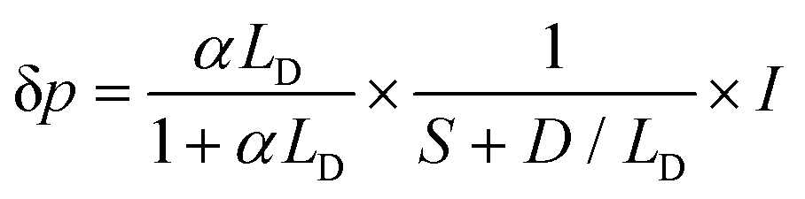
In addition to the optical properties and the energetic levels described in the previous sections, the charge carrier properties of the semiconductor photo(electro)catalyst are also essential. In other words, the charge carrier dynamics need to be well understood in order to know the extent to which the photocatalytic or photoelectrochemical properties of the semiconductor can be improved. Both bulk and surface carrier dynamics are important; several measurement techniques and procedures reported for both are discussed here. Note that although several examples shown here are based on photoelectrode systems, the measurements can also be adapted for particle-based systems by immobilizing the particles on a suitable substrate. The obtained properties are often transferable.Upon photoexcitation, charge carriers that are generated in the bulk of the semiconductor photoelectrodes need to travel to the interfaces (i.e., semiconductor/electrolyte and semiconductor/substrate interfaces). In many cases, especially in metal oxide semiconductors, the optical penetration depth of a semiconductor is much larger than the extent of the SCL (i.e., part of the semiconductor where an electric field is present, as explained in Section 3). Therefore, carrier transport occurs predominantly through a diffusion process rather than drift. A critical property of a semiconductor is the minority carrier diffusion length (LD), which is the distance that minority carriers can travel before they recombine with the majority carriers (either direct band-to-band or through defect-mediated states). One way to determine LD is by performing wavelength-dependent photovoltage or photocurrent measurements. For example, the photovoltage of the sample can be measured using the SPS technique, which has been previously touched upon in Section 2. For an n-type semiconductor with a depletion layer width (wd) much smaller than both the absorption length and the LD, the excess minority carrier (δp) can be expressed in the following form:6,7
 | (7) |
| I = C × (α−1 + LD) | (8) |
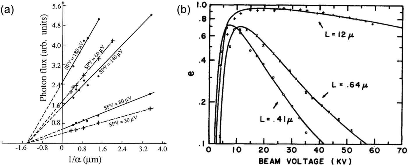 | ||
| Fig. 9 (a) Determination of the diffusion length of (100) InP samples from the intercepts of the photon flux vs. the inverse absorption coefficient (1/α) for several surface photovoltage (SPV) values. Reproduced from ref. 20 with permission from the AIP Publishing, copyright 1976. (b) EBIC collection efficiency (e) vs. beam voltage for Au-GaAs (n-type) Schottky barrier diodes. The GaAs samples have different carrier concentrations: 6.8 × 1015 cm−3 (“+”), 1.3 × 1017 cm−3 (“×”), and 1.1 × 1018 cm−3 (“○”). The diffusion lengths for each sample were obtained by fitting the data points (solid lines) with the model reported by Wu and Wittry.23 Figure a and b: reproduced from ref. 23 with permission from the AIP Publishing, copyright 1978. | ||
In addition to SPS, other spectral approaches have also been performed to extract LD in the form of electron-beam induced current (EBIC) and internal quantum efficiency (IQE) measurements. The EBIC-based method typically requires the formation of a Schottky-junction using a metal layer and the semiconductor of interest. A focused electron beam then bombards the sample, and the collected current density (J) is measured. The collection efficiency (e) can then be determined using the following relationship:
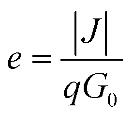 | (9) |
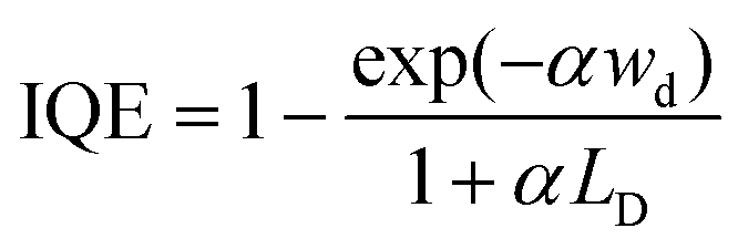 | (10) |
Another somewhat innovative approach was recently reported by Pala et al. using wedge-shaped semiconductor photoelectrodes.25 They showed that for a sample with a thickness (w) much larger than wd, the photocurrent (J) is approximated as a constant factor multiplied by the reciprocal exponential of w/LD (i.e., J ∝ exp(−w/LD)). Using a wedge-shaped semiconductor photoelectrode deposited on a transparent substrate (Fig. 10a), they measured the back-side illuminated photocurrents at various points of the electrode (i.e., different thicknesses). Plotting the natural logarithm of photocurrents as a function of thickness therefore yields a straight line with a slope of −1/LD. Examples of LD determination in Si and BiVO4 wedge photoelectrodes are shown in Fig. 10b and c, respectively. At lower thicknesses, this approximation does not hold (since wd is in the range of w); but the approach was successfully demonstrated for higher thicknesses. It should also be noted that the method should not be wavelength-dependent, as long as the absorption length is much shorter than the diffusion length (see Fig. 10c). Finally, although it is definitely much more efficient using the wedge geometry, the same method can be performed using multiple samples with different thicknesses if deposition of wedge photoelectrodes is not possible.
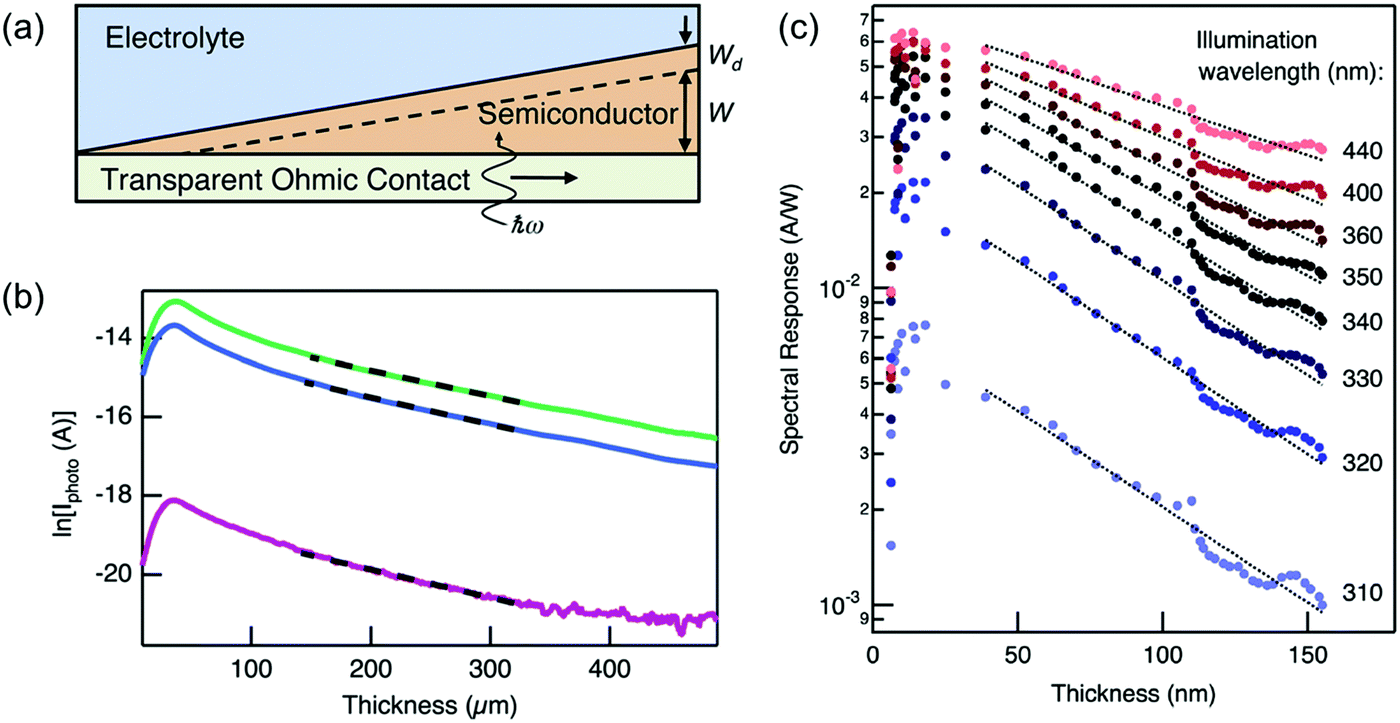 | ||
| Fig. 10 (a) Schematic of the wedge-shaped sample geometry used in the measurement of LD by Pala et al.25 (b) Natural logarithm of photocurrent vs. thickness of a Si wedge illuminated with (top to bottom) 500, 455, and 365 nm light. The LD was calculated to be 168 μm by linear fitting of the data (dashed lines). (c) Similar data as in (b) but for a BiVO4 wedge. The slope is not constant when the illumination wavelength is larger than 340 nm because the absorption length is larger than the LD. A LD of 75 nm was calculated by linear fitting the data at wavelengths of 310, 320, and 330 nm. Figure a–c: reproduced from ref. 25 with permission from The Royal Society of Chemistry, copyright 2014. | ||
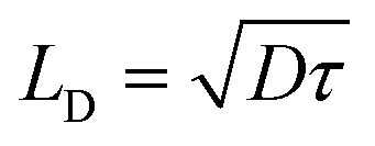
Instead of determining LD directly, one can also calculate LD from the carrier mobility (μ) and lifetime (τ) of the sample. The following expressions can be used:
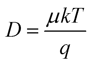 | (11) |
 | (12) |
| σ = qnμ | (13) |
 | (14) |
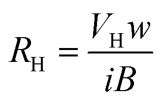
| μH = σ RH | (15) |
Time-resolved photoconductivity measurements using microwave probe signals have also been used in order to determine both μ and τ. In time-resolved microwave conductivity (TRMC), the sample is placed in a microwave cell, and it is subjected simultaneously to a short (typically in the range of a few nanoseconds) laser pulse radiation and a microwave probe. The setup is described in detail elsewhere,30 and a typical schematic of the setup is shown in Fig. 11a. Since microwave interacts with mobile carriers, the photoexcitation by the laser pulse creates a change in the reflected power of the microwave. The normalized change in the microwave power reflected by the cavity upon sample excitation (ΔP/P) can be correlated with the photoinduced change in the conductance of the sample (ΔG), by the following:
 | (16) |
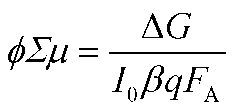 | (17) |
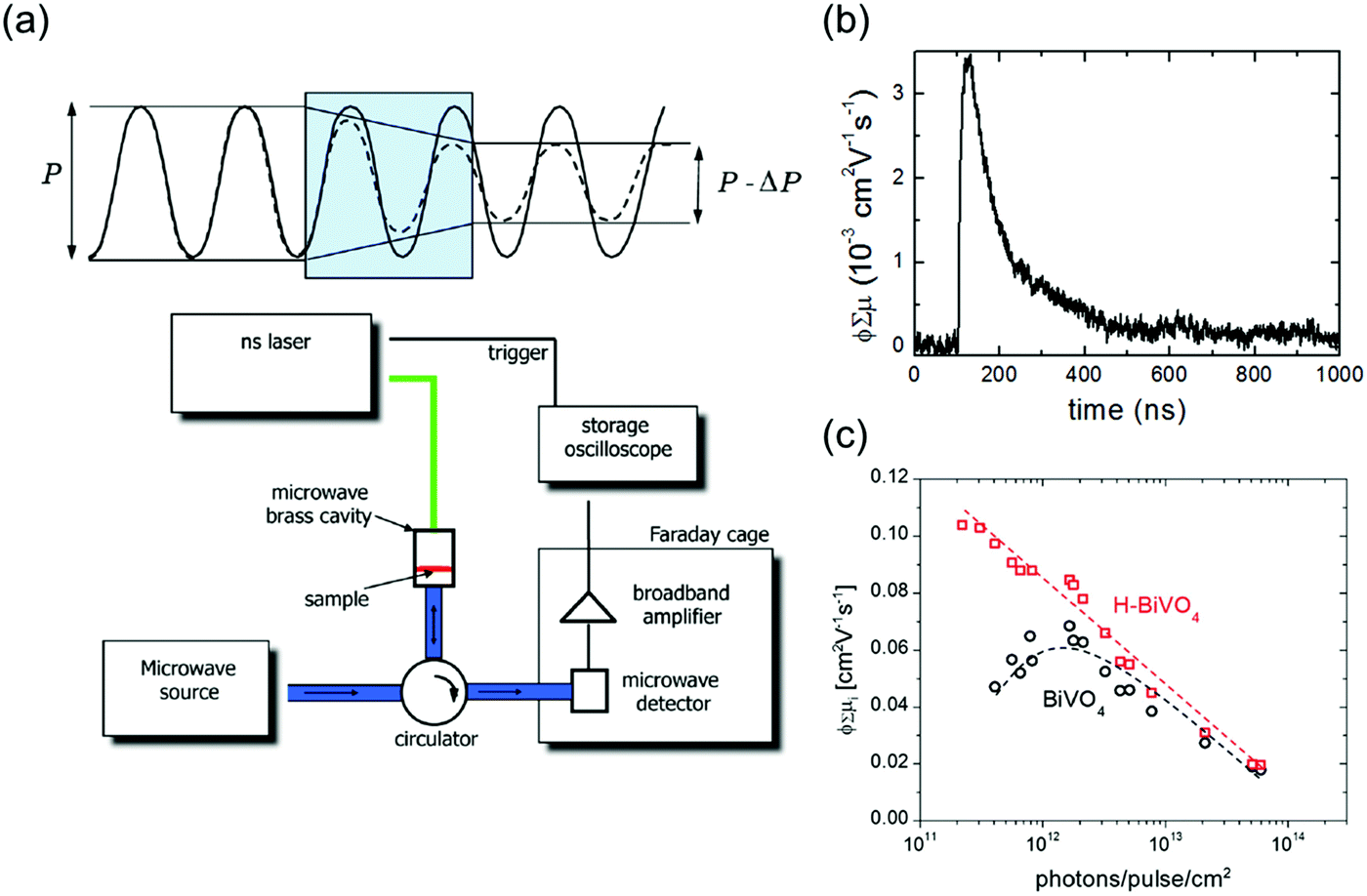 | ||
| Fig. 11 (a) (top) Illustration of the attenuation of microwaves due to propagation through a weakly conducting medium. (bottom) Schematic representation of a typical TRMC setup. Reproduced from ref. 30 with permission from the American Chemical Society, copyright 2013. (b) TRMC signal (ϕΣμ vs. time) measured for undoped spray-pyrolyzed BiVO4. Reproduced from ref. 31 with permission from the American Chemical Society, copyright 2013. (c) Maximum observed TRMC signals (maximum ϕΣμ) as a function of incident photons for pristine and hydrogen-treated BiVO4. Reproduced from ref. 32 with permission from WILEY-VCH Verlag GmbH & Co. KGaA, Weinheim, copyright 2017. | ||
A typical ϕΣμ plot as a function of time (here taken from a BiVO4 photoanode as an example) is shown in Fig. 11b. From the peak of the plot (i.e., the maximum ϕΣμ), the μ value is typically obtained. The decay of the curve is usually fitted with a single-/multi-exponential or a power-law function, from which τ can be determined. It should be noted that microwave is sensitive to all types of carriers, i.e., specific electron and hole mobility values cannot be distinguished. If the electron and hole effective masses in the sample are known (e.g., from DFT calculation), each mobility value can be calculated, but this is again under the assumption that both electron and hole have the same carrier scattering time. Nevertheless, the results obtained from TRMC can serve as a good estimate for the μ and τ—and therefore the LD—of a semiconducting photoelectrode.
Further information that can be obtained from TRMC is whether trap states are present and trap-assisted recombination affects the carrier transport in a photoelectrode. This is done by performing TRMC measurement at various laser pulse intensities and plotting the mobility values (i.e., the maximum ϕΣμ) vs. the pulse intensities (i.e., I0). When trap states are present, the mobility first increases with increasing pulse intensity until it reaches a maximum; beyond this point, it again decreases with higher pulse intensity. This has been attributed to the competition between trap filling and higher order recombination.30,32 Prior to the maximum point, the concentration of trap states is higher than the number of absorbed photons. The mobility, therefore, increases until the entire trap states are filled, and it reaches a maximum. Beyond that, the mobility decreases due to fast non-geminate higher order recombination during the laser pulse. On the other hand, when no trap states are present, the mobility is expected to monotonically decrease with increasing pulse intensity, due to the same higher order recombination, i.e., no maximum is observed. Fig. 11c shows an example from a recent result of a pristine and a hydrogenated BiVO4 photoanode.32 A clear maximum is observed for the pristine photoanode, indicating the presence of trap states, whereas the hydrogenated photoanode shows only a monotonic decrease of mobility with laser pulse intensity. The density of trap states can also be estimated by dividing the laser pulse intensity at which the maximum point is located with the thickness of the photoanode. Using the example from Fig. 11c, since the maximum point is located at ∼2 × 10¹² pulse−1 cm−2 and the thickness of the photoanode is ∼200 nm, the density of trap states is estimated to be ∼1017 cm3.
Although TRMC provides advantages that it directly measures the actual photoconductivity, and it is also applicable to indirect-gap semiconductors (unlike luminescence), several disadvantages remain. First, as already mentioned above, it does not allow for the differentiation between the majority and minority carriers. An approximation can be made, but this has to be done with extra care and assumptions. Second, the sample needs to be deposited on a non-conductive substrate (e.g., quartz, sapphire). This is of course different than the operando condition of the photoelectrode during the photoelectrochemical measurements. External potentials cannot be applied, and deposition on conducting (e.g., FTO-coated glass) and non-conducting substrates may result in different growth and properties of the sample. Several groups have attempted to perform in situ microwave reflection measurements in a photoelectrochemical cell using a conducting substrate that is selectively etched,33 but the sensitivity of the measurement is much lower as compared to when a cavity cell is used. A combination of the TRMC results and other techniques, as described earlier, is therefore still needed to provide a complete carrier dynamics picture of a photoelectrode.
Once the charge carriers (electrons or holes) reach the interface, they can either recombine or transfer to the electron acceptor/donor in the electrolyte (e.g., water reduction/oxidation). Apart from the bulk charge carrier properties such as LD, μ, and τ that have hitherto been discussed, the rate of the interfacial processes is also of interest and can be determined using time-resolved or frequency-resolved techniques. Examples of time-resolved techniques are transient absorption spectroscopy (TAS) and photo-induced absorption (PIA) spectroscopy. Both techniques use an optical illumination (pump) to generate charge carriers in the semiconductor and an additional optical illumination (probe) to monitor the fate of these charge carriers. The charge carriers therefore need to show distinct optical signatures in the measured spectra. This is not always the case, but measurements in the presence of hole and electron scavengers in the electrolyte can help identify these signatures.34 In TAS, both the pump and probe are typically short laser pulses (fs–ns) which are separated by a certain delay. By varying the delay between the pump and the probe light, the optical absorption change (ΔA) in the sample can be measured as a function of time. Since water oxidation and reduction are typically slow processes, it is therefore important to be able to measure with a relatively long delay (μs–s). Based on the decay of the ΔA, the lifetime of the charge carriers accumulating at the interface and the rate constant for water oxidation or reduction can then be determined.34 PIA, on the other hand, usually uses much longer optical pulses (seconds) with an LED as the pump, while the probe is continuous illumination (e.g., Xe lamp with a monochromator). Fig. 12a shows the schematic of a typical PIA setup. The PIA signal, ΔA, as well as the photocurrent of the sample are then monitored as the LED turns on and off. Fig. 12b and c show the PIA signals and photocurrents from a report on a BiVO4 photoanode by Ma et al.35 In that study, they were able to quantify the amount of surface hole density by correlating the PIA signals and the photocurrent transients. Using a simple kinetic model,35 the relationship between the photocurrent and the surface hole density could be derived, and the rate constant for water oxidation as well as the reaction order (α) were determined. It was found that water oxidation on the BiVO4 photoanode undergoes a transition from first to third order reaction at a surface hole density of 1 nm−2 (Fig. 12d).
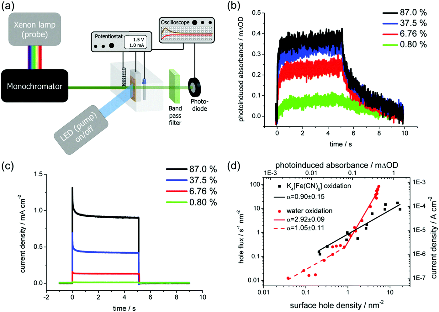 | ||
| Fig. 12 (a) Schematic illustration of a typical photoinduced absorption (PIA) spectroscopy setup. (b) PIA signal and (c) photocurrent density of a BiVO4 photoanode simultaneously measured under 5 s pulsed 365 nm LED illumination (with varying illumination intensity—100% corresponds to the intensity of AM1.5 illumination) under water oxidation conditions at 1.7 V vs. RHE. (d) Relationship between the photocurrent density and the surface hole density (determined from the PIA signal). Fitting the data with a kinetic model reveals the reaction order (α) for water oxidation on BiVO4. Figure b–d: reproduced from ref. 35 with permission from the American Chemical Society, copyright 2016. | ||
Instead of time-resolved measurements, the charge carrier dynamics at the semiconductor/electrolyte interface can also be investigated using frequency-resolved techniques. An example is intensity modulated photocurrent spectroscopy (IMPS). Here, the sample is subjected to a small-amplitude modulated illumination (e.g., using LED), which results in a modulated photocurrent. A schematic of the setup is shown in Fig. 13a. The frequency of the resulting modulated photocurrent is the same as that of the illumination, but the magnitude and phase are generally different. This complex photocurrent response consists of the sum of the minority and majority carrier currents. By scanning the frequency during the measurements, a Nyquist plot can be constructed showing the real and imaginary parts of the photocurrent. An example is shown in Fig. 13b for an n-type semiconductor (i.e., photoanode). The lower quadrant semicircle at higher frequencies represents the attenuation by the total cell series resistance (R) and cell capacitance (Ccell).36,37 The cell capacitance is a combination of the space charge and Helmholtz capacitances (CSC and CH), but CH can usually be neglected for materials with moderate charge carrier density. The upper quadrant semicircle at lower frequencies is usually called the recombination semicircle. This is based on a simplified model, described in detail in the study by Peter et al.,36,37 which assigns this semicircle to the competition between charge transfer (i.e., hole injection into the electrolyte for a photoanode and electron injection for a photocathode) and charge recombination at the semiconductor/electrolyte interface. The semicircle reaches a maximum when the frequency matches the characteristic relaxation constant of the system:
| ωmax = ktr + krec | (18) |
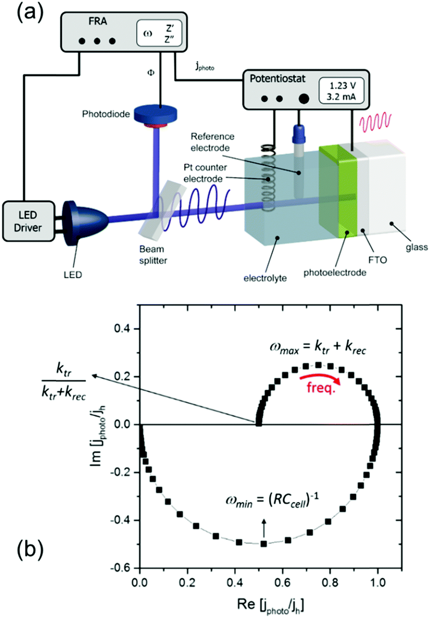 | ||
| Fig. 13 (a) Schematic diagram of a typical IMPS setup. (b) An example of a complex photocurrent or an IMPS spectrum for an n-type semiconductor. The recombination semicircle is shown in the upper quadrant, and the attenuation semicircle appears in the lower quadrant. Using a model of Peter et al.,36 the charge transfer rate constant (ktr) and the surface recombination rate constant (krec) can be obtained based on the multiple points of such a spectrum. Figure a and b: reproduced from ref. 37 with permission from The Royal Society of Chemistry, copyright 2017. | ||
where ktr is the reaction rate constant for charge transfer, and krec is the reaction rate constant for charge recombination. At the high frequency intercept with the real photocurrent axis, the fast modulation freezes the charge recombination; normalizing the photocurrent at this point against the hole current for a photoanode (jphoto/jh) therefore gives a value of 1. The fraction of holes at the surface that is injected into the electrolyte can be determined from the low frequency intercept (LFint) with the real photocurrent axis:
 | (19) |
Using eqn (18) and (19), both ktr and krec can therefore be determined. Details of the model (assumptions, limitations, etc.) and the derivation of the equations can be found in the literature.36,37
It is important to note that care should be taken in interpreting the absolute value of ktr and krec. For a simple one-electron charge transfer reaction, these rate constants are true rate constants (the unit is s−1). It is however more complicated for the case of multi-step charge transfer reactions, such as water oxidation and reduction. In this case, ktr and krec should be interpreted as phenomenological rate parameters that are functions of the rate constants of the elementary steps.38 If the reaction mechanism is known, the relationship can in principle be derived,38 but this has not been attempted, especially for the water oxidation reaction. Nevertheless, the equations above can still be used to analyze the IMPS response and distinguish charge transfer and recombination processes. ktr and krec are therefore usually called pseudo first-order rate constants in the literature.37
5. Combinatorial/in situ approaches
Most of the characterization tools discussed in Sections 2–4 are macroscopic, that is, the measured properties are generally the averages of the bulk sample that may not be representative of the isolated/local microstructures. Typically, the properties of a semiconductor photo(electro)catalyst do not only rely on the bulk composition but also greatly on the surface crystallinity and structure such as the surface atomic arrangement and coordination. With the pre-eminence of nanomaterials in photo(electro)catalysis, advancement of research tools with high selectivity, sensitivity, and spatial resolution is essential to provide direct experimental evidence for surface-dependent properties via micro-region measurements. In particular, more than one tool can be combined to provide more comprehensive insight into various aspects of the photo(electro)catalyst. For example, a light source can be incorporated into a conductive atomic force microscope (i.e., photoassisted conductive atomic force microscopy PC-AFM) to enable local determination of the optoelectronic and the interfacial charge transfer properties of a photocatalyst.39 Coupling of spatially resolved surface photovoltage spectroscopy (SRSPS) with Kelvin probe force microscopy (KPFM) has been demonstrated to be useful in showing the highly anisotropic photoinduced charge separation on the different crystal facets of a single photocatalyst.40 The combination of optical and electrochemical techniques such as spatially and temporally resolved single-particle spectroelectrochemistry is also helpful in revealing the carrier dynamics of a photocatalyst in relation to its crystal faces.41Another major downside of the techniques outlined in preceding sections is that the measurements are typically done before and after the photocatalytic or photoelectrochemical reaction. This greatly obscures the understanding of the structure–property relationship that could potentially change during the reaction. In situ techniques have thus come forth in order to obtain a direct relationship between the optoelectronic/electrochemical and the physicochemical properties (e.g., particle size, crystallinity, morphology, crystal structure, and surface chemical states) of a semiconductor (down to nanosize scale) during a reaction. One great example in line with the scope of this review is the engineering of in situ transmission electron microscopy (TEM),42,43 whereby the TEM column or specimen holder is modified to enable light illumination and/or emitted light collection to enable real-time measurements of nanostructure properties in response to light in tandem with high resolution imaging of the material. Fig. 14a illustrates the schematic of a typical opto-TEM setup that enables in situ illumination and light collection by incorporating a combination of mirrors, lenses, and optical fibers into the TEM column. Detailed explanation of the setup is described elsewhere.42 Such a system has also been demonstrated to produce a smaller light probe (10 μm in diameter) with near-field light by positioning a silver-coated tungsten tip normal to the optical path of laser light (Fig. 14b).43 Without modification to the TEM column, light transmission can also be achieved using an opto-compatible TEM holder, in which lenses or optical fibers are integrated. Accessibility to various opto-compatible TEM holders and opto-TEM setups has made in situ PL, Raman, and photocurrent spectroscopy measurements inside TEM viable.
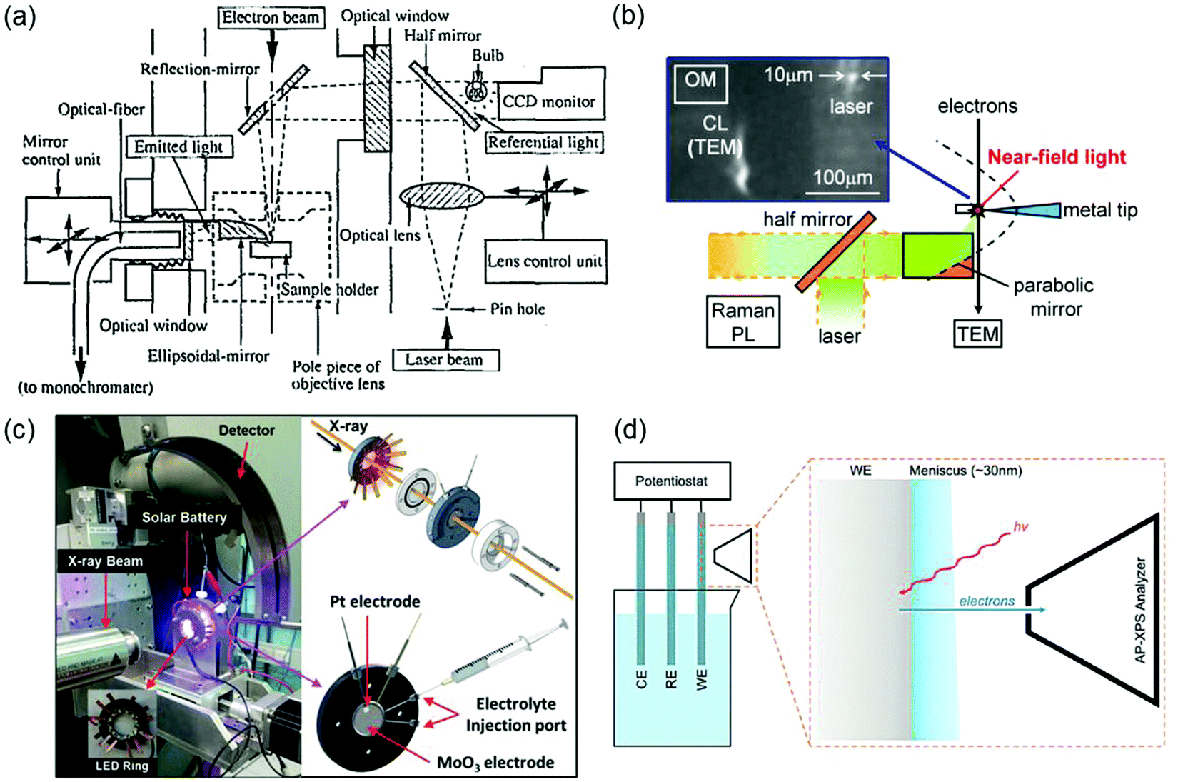 | ||
| Fig. 14 (a) Schematic of a typical opto-TEM setup with in situ illumination and emitted light collection. Reproduced from ref. 42 with permission from the AIP Publishing, copyright 1995. (b) An opto-TEM setup with in situ near-field photoexcitation. Reproduced from ref. 43 with permission from Elsevier B.V., copyright 2013. (c) Operando XRD setup with a customized LED integrated photoelectrochemical cell. Reproduced from ref. 44 with permission from WILEY-VCH Verlag GmbH & Co. KGaA, Weinheim, copyright 2017. (d) A typical three-electrode electrochemical setup for AP-XPS measurement of a working electrode (WE) surface covered by a meniscus layer of the electrolyte. RE: reference electrode; CE: counter electrode. Reproduced from ref. 45 with permission from the PCCP Owner Societies, copyright 2015. | ||
In situ and operando X-ray powder diffraction (XRD) and ambient-pressure photoemission spectroscopy measurements under operating (photo)electrochemical conditions have also been carried out recently. Fig. 14c shows an operando synchrotron XRD setup using a tailor-made doughnut shaped photoelectrochemical cell. While the LED integrated open center cell enables illumination of the solar battery consisting of MoO3 and Pt as the respective photoanode and counter electrodes, in situ XRD measurement allows real-time visualization of the structural evolution of MoO3 due to light-induced photointercalation.44 The development of ambient-pressure XPS (AP-XPS), on the other hand, allows in situ characterization of electrode/electrolyte interfaces that are crucial in (photo)electrochemical systems.45,46 A typical setup of AP-XPS is illustrated in Fig. 14d. In particular, the use of tender X-rays with energies between soft and hard X-rays (∼2–7 keV) facilitates operando XPS characterization of the chemical changes at the electrode/electrolyte interfaces. However, due to the limited photoelectron mean free path, the electrolyte thickness in such ambient-pressure tender XPS method needs to be kept in the range of 20–30 nm. One common approach to obtain a thin layer of electrolyte film is via the dip-and-pull technique, whereby the working electrode is dipped and pulled from the electrolyte reservoir therefore creating an electrolyte meniscus (see Fig. 14d).
6. Summary
An overview of the current experimental techniques accessible for scrutinizing the three discrete key properties of a photoactive semiconductor, including the band gap (Eg), absolute potentials of the conduction band minimum (ECB) and the valence band maximum (EVB), and charge carrier dynamics within the bulk and at the surface of the semiconductor (i.e., diffusion length LD, mobility μ, lifetime τ, surface charge recombination rate, and interfacial charge transfer rate), is provided. Technology advancement, mainly in the past few decades, has enabled the development of various sophisticated characterization tools with high spatial, temporal, and spectral resolutions as well as high sensitivity and selectivity. Although we intended to present state-of-the-art experimental characterization techniques in addition to the common methods related to the determination of all key aspects of photo(electro)catalysts, it should be realized that the list of measurement techniques described herein is not exhaustive. For instance, time-resolved THz spectroscopy has been used to investigate the bulk charge carrier dynamics (i.e., to determine μ and τ),28 and photoelectrochemical impedance spectroscopy (PEIS) has been widely used to determine the rate constants for the processes at the semiconductor/electrolyte interface.47 Readers are recommended to refer to the excellent review papers and books that provided details of these additional techniques.48–50Note that despite the restriction of several methods to electrode-based systems, they are generally applicable for measurements on particulate materials by proper transformation of the powders into thin films on suitable substrates since the attained properties are often transferable to particle-based systems. Given the inherent limitations of each macroscopic technique, a combination of numerous analysis approaches is typically essential to provide a more complete and concrete evaluation of the specific aspect of a semiconductor. In particular, direct measurements of local optoelectronic properties and charge carrier dynamics in relation to the surface structure of nanostructures have been demonstrated to be feasible. The breakthrough of experimental characterization tools is undoubtedly the invention of in situ and/or operando measurements, allowing real-time evaluation of semiconductor properties.
Conflicts of interest
The authors declare no conflict of interest.Acknowledgements
H. L. Tan, F. F. Abdi, and Y. H. Ng thank the Australian Research Council for financial support through Discovery Projects DP180102540 and DP170102895.References
- H. L. Tan, R. Amal and Y. H. Ng, J. Mater. Chem. A, 2017, 5, 16498–16521 RSC.
- S. Tandon and J. Gupta, Phys. Status Solidi B, 1970, 38, 363–367 CrossRef CAS.
- J. Tauc, in Optical Properties of Solids ed. F. Abeles, North-Holland Publ. Co, Amsterdam, 1972 Search PubMed.
- E. Davis and N. Mott, Philos. Mag., 1970, 22, 0903–0922 CrossRef CAS.
- J. H. Nobbs, Color. Technol., 1985, 15, 66–75 Search PubMed.
- L. Kronik and Y. Shapira, Surf. Interface Anal., 2001, 31, 954–965 CrossRef CAS.
- L. Kronik and Y. Shapira, Surf. Sci. Rep., 1999, 37, 1–206 CrossRef CAS.
- M. Anpo and M. Che, Advances in Catalysis, Elsevier, 1999, vol. 44, pp. 119–257 Search PubMed.
- C. Li and Y. Yue, Nanotechnology, 2014, 25, 435703 CrossRef PubMed.
- S. R. Morrison, Electrochemistry at semiconductor and oxidized metal electrodes, Springer, US, 1980 Search PubMed.
- R. Beranek, Adv. Phys. Chem., 2011, 2011, 786759 Search PubMed.
- D. Cahen and A. Kahn, Adv. Mater., 2003, 15, 271–277 CrossRef CAS.
- M. Jakob, H. Levanon and P. V. Kamat, Nano Lett., 2003, 3, 353–358 CrossRef CAS.
- N. Dimitrijevic, D. Savic, O. Micic and A. Nozik, J. Phys. Chem., 1984, 88, 4278–4283 CrossRef CAS.
- J. Gandia, M. Pujadas and P. Salvador, J. Electroanal. Chem. Interfacial Electrochem., 1988, 244, 69–79 CrossRef CAS.
- E. Kraut, R. Grant, J. Waldrop and S. Kowalczyk, Phys. Rev. Lett., 1980, 44, 1620 CrossRef CAS.
- S. A. Chambers, T. Droubay, T. C. Kaspar and M. Gutowski, J. Vac. Sci. Technol., B: Microelectron. Nanometer Struct.--Process., Meas., Phenom., 2004, 22, 2205–2215 CrossRef CAS.
- W.-J. Chun, A. Ishikawa, H. Fujisawa, T. Takata, J. N. Kondo, M. Hara, M. Kawai, Y. Matsumoto and K. Domen, J. Phys. Chem. B, 2003, 107, 1798–1803 CrossRef CAS.
- S. Trasatti, Pure Appl. Chem., 1986, 58, 955–966 CAS.
- S. S. Li, Appl. Phys. Lett., 1976, 29, 126–127 CrossRef CAS.
- M. Saritas and H. D. McKell, J. Appl. Phys., 1988, 63, 4561–4567 CrossRef CAS.
- T. Dittrich, F. Lang, O. Shargaieva, J. Rappich, N. Nickel, E. Unger and B. Rech, Appl. Phys. Lett., 2016, 109, 073901 CrossRef.
- C. Wu and D. Wittry, J. Appl. Phys., 1978, 49, 2827–2836 CrossRef CAS.
- T. Gokmen, O. Gunawan and D. B. Mitzi, J. Appl. Phys., 2013, 114, 114511 CrossRef.
- R. A. Pala, A. J. Leenheer, M. Lichterman, H. A. Atwater and N. S. Lewis, Energy Environ. Sci., 2014, 7, 3424–3430 RSC.
- A. J. Rettie, W. D. Chemelewski, D. Emin and C. B. Mullins, J. Phys. Chem. Lett., 2016, 7, 471–479 CrossRef CAS PubMed.
- O. Gunawan, S. R. Pae, D. M. Bishop, Y. S. Lee, Y. Virgus, N. J. Jeon, J. H. Noh, X. Shao, T. Todorov and D. B. Mitzi, 2018, arXiv preprint arXiv:1802.07910.
- M. Ziwritsch, S. Müller, H. Hempel, T. Unold, F. F. Abdi, R. van de Krol, D. Friedrich and R. Eichberger, ACS Energy Lett., 2016, 1, 888–894 CrossRef CAS.
- D. Emin, in The Hall Effect and Its Applications, ed. C. L. Chien and C. R. Westgate, Springer, Boston, MA, 1980, pp. 281–298 Search PubMed.
- T. J. Savenije, A. J. Ferguson, N. Kopidakis and G. Rumbles, J. Phys. Chem. C, 2013, 117, 24085–24103 CrossRef CAS.
- F. F. Abdi, T. J. Savenije, M. M. May, B. Dam and R. van de Krol, J. Phys. Chem. Lett., 2013, 4, 2752–2757 CrossRef CAS.
- J. W. Jang, D. Friedrich, S. Müller, M. Lamers, H. Hempel, S. Lardhi, Z. Cao, M. Harb, L. Cavallo and R. Heller, Adv. Energy Mater., 2017, 7, 1701536 CrossRef.
- H. K. Dunn, L. M. Peter, S. J. Bingham, E. Maluta and A. B. Walker, J. Phys. Chem. C, 2012, 116, 22063–22072 CrossRef CAS.
- S. R. Pendlebury, M. Barroso, A. J. Cowan, K. Sivula, J. Tang, M. Grätzel, D. Klug and J. R. Durrant, Chem. Commun., 2011, 47, 716–718 RSC.
- Y. Ma, C. A. Mesa, E. Pastor, A. Kafizas, L. Francàs, F. Le Formal, S. R. Pendlebury and J. R. Durrant, ACS Energy Lett., 2016, 1, 618–623 CrossRef CAS.
- E. Ponomarev and L. Peter, J. Electroanal. Chem., 1995, 396, 219–226 CrossRef.
- C. Zachäus, F. F. Abdi, L. M. Peter and R. van De Krol, Chem. Sci., 2017, 8, 3712–3719 RSC.
- L. Peter, E. Ponomarev and D. Fermin, J. Electroanal. Chem., 1997, 427, 79–96 CrossRef CAS.
- S. Wang, X. Zhang, G. Cheng, X. Jiang, Y. Li, Y. Huang and Z. Du, Chem. Phys. Lett., 2005, 405, 63–67 CrossRef CAS.
- J. Zhu, F. Fan, R. Chen, H. An, Z. Feng and C. Li, Angew. Chem., 2015, 127, 9239–9242 CrossRef.
- T. Tachikawa, T. Ochi and Y. Kobori, ACS Catal., 2016, 6, 2250–2256 CrossRef CAS.
- Y. Ohno and S. Takeda, Rev. Sci. Instrum., 1995, 66, 4866–4869 CrossRef CAS.
- Y. Ohno and I. Yonenaga, Appl. Surf. Sci., 2014, 302, 29–31 CrossRef CAS.
- S. N. Lou, N. Sharma, D. Goonetilleke, W. H. Saputera, T. M. Leoni, P. Brockbank, S. Lim, D. W. Wang, J. Scott and R. Amal, Adv. Energy Mater., 2017, 7, 1700545 CrossRef.
- C. H. Wu, R. S. Weatherup and M. B. Salmeron, Phys. Chem. Chem. Phys., 2015, 17, 30229–30239 RSC.
- D. E. Starr, M. Favaro, F. F. Abdi, H. Bluhm, E. J. Crumlin and R. van de Krol, J. Electron Spectrosc. Relat. Phenom., 2017, 221, 106–115 CrossRef CAS.
- B. Klahr, S. Gimenez, F. Fabregat-Santiago, J. Bisquert and T. W. Hamann, J. Am. Chem. Soc., 2012, 134, 16693–16700 CrossRef CAS PubMed.
- R. Ulbricht, E. Hendry, J. Shan, T. F. Heinz and M. Bonn, Rev. Mod. Phys., 2011, 83, 543 CrossRef CAS.
- L. Bertoluzzi and J. Bisquert, J. Phys. Chem. Lett., 2012, 3, 2517–2522 CrossRef CAS PubMed.
- E. Barsoukov and J. R. Macdonald, Impedance Spectroscopy: Theory, Experiment, and Applications, John Wiley & Sons, Hoboken, NJ, 2018 Search PubMed.
Footnote |
| † Present address: Department of Applied Chemistry, Faculty of Engineering, Kyushu University, Nishi-ku, Fukuoka 819-0395, Japan. E-mail: hui.ling.tan.291@m.kyushu-u.ac.jp |
| This journal is © The Royal Society of Chemistry 2019 |