
 Open Access Article
 This Open Access Article is licensed under a Creative Commons Attribution-Non Commercial 3.0 Unported Licence
Growth of highly oriented MoS2via an intercalation process in the graphene/SiC(0001) system
Paweł Piotr
Michałowski
 *a,
Piotr
Knyps
a,
Paweł
Ciepielewski
a,
Piotr A.
Caban
a,
Ewa
Dumiszewska
a,
Grzegorz
Kowalski
b,
Mateusz
Tokarczyk
b and
Jacek M.
Baranowski
a
*a,
Piotr
Knyps
a,
Paweł
Ciepielewski
a,
Piotr A.
Caban
a,
Ewa
Dumiszewska
a,
Grzegorz
Kowalski
b,
Mateusz
Tokarczyk
b and
Jacek M.
Baranowski
a
aŁukasiewicz Research Network - Institute of Electronic Materials Technology, Wólczyńska 133, 01-919 Warsaw, Poland. E-mail: pawel.michalowski@itme.edu.pl
bFaculty of Physics, University of Warsaw, Pasteura 5, 02-093 Warsaw, Poland
First published on 3rd September 2019
Abstract
A method of growing highly oriented MoS2 is presented. First, a Mo film is deposited on a graphene/SiC(0001) substrate and the subsequent annealing of it at 750 °C leads to intercalation of Mo underneath the graphene layer, which is confirmed by secondary ion mass spectrometry (SIMS) measurements. Formation of highly oriented MoS2 layers is then achieved by sulfurization of the graphene/Mo/SiC system using H2S gas. X-ray diffraction reveals that the MoS2 layers are highly oriented and parallel to the underlying SiC substrate surface. Further SIMS experiments reveal that the intercalation process occurs via the atomic step edges of SiC and Mo and S atoms gradually diffuse along SiC atomic terraces leading to the creation of the MoS2 layer. This observation can be explained by a mechanism of highly oriented growth of MoS2: nucleation of the crystalline MoS2 phase occurs underneath the graphene planes covering the flat parts of SiC steps and Mo and S atoms create crystallization fronts moving along terraces.
1 Introduction
The drive towards miniaturization of electronic devices leads to a tendency to introduce new technologies connected with graphene and other 2D materials such as transition metal dichalcogenides (TMDs). Among TMDs MoS2 has emerged as the material which has been the most extensively studied.1–9 MoS2 has also been studied for application in future electronic devices.10,11Early investigations of MoS2 were based on stacking the layered material using wet or dry transfer methods.12 This strategy requires a complicated transfer process which generates defects and leaves residues at the interface, and is not promising for obtaining large wafer scale material suitable for device fabrication.
Chemical Vapour Deposition (CVD) epitaxy seems to be the natural strategy for growth of large area MoS2 and other TMD layers. There have been several efforts and reports on CVD growth of MoS2 on insulating substrates.13–18 Among epitaxial methods direct growth of MoS2 with the use of a Mo film deposited on an insulating substrate and controllable sulfurization was also reported.19,20 In most cases SiO2 substrates have been used on which triangular shape MoS2 grains have been obtained, for example as shown in recent work.21 However, only recently has it been shown that wafer scale large area continuous MoS2 layers are possible to grow. This was achieved by eliminating substrates containing oxygen. Oxygen released from such substrates plays a disruptive role in the increase of the grain size of MoS2 during layer growth.22 Therefore, use of substrates without oxygen such as BN/Al2O3 epilayers is beneficial. Furthermore, integration of several 2D materials is seen as the best route to fabricate novel heterostructure devices.23
In this work we have used a new kind of substrate, graphene grown on SiC(0001). Our growth method of MoS2 was connected with evaporation of a Mo film onto graphene covered 6H-SiC(0001) substrates. The process of CVD growth of graphene on SiC(0001) is well known.24 Epitaxial growth of graphene on SiC(0001) is connected with formation of a buffer layer underneath the graphene.25,26 The buffer layer comprises a carbon layer that is covalently bonded to the underlying SiC substrate and does not show graphitic electronic properties. The electronically inactive reconstructed buffer layer on SiC(0001) may be converted into quasi-free-standing monolayer graphene after hydrogen intercalation.27,28 Intercalation of hydrogen decouples the buffer layer from its substrate and forms weakly coupled bilayer graphene. Hydrogen intercalation opened up the possibility to produce quasi-free-standing epitaxial graphene on large SiC wafers. It is known that CVD grown graphene on SiC(0001) after hydrogen intercalation produces p-type layers with higher carrier mobilities than grown on metal substrates.
It is known that the process of intercalation of atoms under a graphene layer is not only limited to hydrogen. It was already reported that intercalation of metals under graphene on SiC(0001) can take place as well. Intercalation of transition metals such as Fe,29 Mn,30 and Co31 was reported. Also, other elements such as Au,32 Ge,33 and Ca34 were successfully intercalated underneath graphene layers grown on SiC(0001). There is an open question of how atoms of these elements incorporate underneath the graphene layer. Most likely, they go through graphene defects on step edges of the SiC surface. This suggestion is supported by evidence that for ultra-thin Co films magnetic wires are formed at the step edges.31 Furthermore, it is believed that graphene on SiC(0001) grows in a contionous fashion over terraces and step edges as well. Indeed TEM measurements show that graphene drapes over steps like a blanket.35 However, there is evidence of a polycrystalline nature of graphene layers as well. In particular grain boundaries are expected to alter the electronic transport in graphene.36 A theory developed on the formation of grain boundaries in graphene has shown that different orientations of graphene can be joined together into a contionous layer via boundaries with seven-fold and five-fold rings.36 Such seven-fold rings can create openings in the graphene lattice suitable for intercalation of atoms. Therefore, it may be expected that the orientaion of the graphene lattice on terraces and step edges will be different and the presence of seven-fold rings on step edges will create channels for intercalation. Our secondary ion mass spectrometry (SIMS) results directly show that such a mechanism of intercalation in the case of Mo may well happen.
The present work describes formation and investigation of MoS2 layers grown underneath a graphene layer on 6H-SiC(0001). Successful growth of MoS2 underneath a graphene layer obtained on 6H-SiC(0001) was created in two steps. The first one was connected with intercalation of a molybdenum layer under the graphene layer. Successful intercalation of Mo was confirmed by SIMS measurements. The next step was sulfurization of the molybdenum and formation of MoS2 under the graphene layer. Formation of the MoS2 layer was verified by SIMS, X-ray diffraction and Raman spectroscopy. The SIMS measurements directly showed that the MoS2 layer was located underneath the graphene layer. The presence and highly oriented character of the grown MoS2 layer was shown by X-ray diffraction.
2 Experimental
Sample preparation
Graphene layers were grown on 6H-SiC(0001) by Chemical Vapour Deposition (CVD) methods at 1600 °C under an argon laminar flow in an Aixtron VP508 hot-wall reactor. Semi-insulating on-axis oriented 6H-SiC (0001) substrates were etched in hydrogen at 1600 °C prior to the epitaxy process. The graphene growth was controlled by the Ar pressure, Ar linear flow velocity, and reactor temperature as described previously.24 The intercalation of hydrogen was achieved by the process of changing the gas from argon to hydrogen at a temperature of 1100 °C during the sample cooling.28Thin Mo film deposition was done by an E-beam PVD deposition process. Deposition of Mo metal was done under a 5 × 10⁻⁷ Torr pressure. The evaporated Mo film ranged from 0.4 to 1.0 nm thickness. After this stage, Mo sputtered samples were placed in the high temperature zone of a Chemical Vapour Deposition (CVD) reactor for sulfurization to form the MoS2 film. H2S was used as the source of sulphur and H2 as the carrier gas. The sulfurization process took place at a 750 °C temperature for 15 minutes. After the growth, the furnace was naturally cooled down to 150 °C for evaporation of excess sulphur from the surface of the sample.
Characterization
In this work all SIMS measurements were performed employing a CAMECA SC Ultra instrument under an ultra-high vacuum (UHV), usually of 4 × 10⁻¹⁰ mbar. Sufficient depth resolution was obtained for negative ion detection mode by using a low impact energy of 100 eV for a Cs+ primary beam rastered over 250 × 250 μm2. The analysis area was limited to 200 × 200 μm2. The SC Ultra tool is able to achieve such low impact energies due to the EXLIE (EXtra Low Impact Energy) technology, in the case of which a primary floating column concept is used.37 In this notion, contrary to standard SIMS tools, the primary column has a “floating voltage”' instead of a grounded voltage level between the space at any two lenses inside the column and thus primary ions are slowed down at the end of the column, maintaining favourable conditions for ion acceleration and beam stability. The ion beam on the sample in the SC Ultra tool has a square shape and due to the “variable rectangular shape concept”' forms a homogeneous spot. The primary beam at a working point in the SC Ultra is formed by two stencils – well-shaped apertures. While the first one is used to choose the most intense and homogeneous part of the ion beam, the second one changes the size of the spot. These innovations allow one to use the low impact energy of primary ions with high sensitivity for all elements measured, a high depth resolution (below 1 nm), and a high dynamic range with a low sputter rate.38,39 All experiments were repeated several times with the primary beam oriented parallel, perpendicular and at several intermediate angles to the steps of SiC but no significant difference was found.Room temperature Raman measurements were performed on a Renishaw inVia Raman microscope using a 532 nm wavelength obtained from a Nd:YAG laser. The size of the laser spot was about 0.5 μm and the power was below 0.1 mW to avoid the destruction of MoS2 layers. The laser was focused on the sample using a ×100 objective and numerical aperture NA = 0.9 in a backscattering geometry.
Investigation of the crystallographic structure and quality of the Gr/MoS2/SiC heterostructure was done by X-ray diffraction measurements using an X'pert Phillips diffractometer equipped with a standard laboratory X-ray source (Cu Kα radiation) and parallel beam Bragg reflection mirror.
3 Results and discussion
SIMS is a very precise analytical technique for determining the elemental composition of a sample40–45 and we have already showed that it can be used to characterize 2D materials like graphene,46–50 BN thin films51,52 and MoS2 films.22 Therefore SIMS was a natural choice to monitor the intercalation process.As it can be seen in Fig. 1a Mo is evaporated on top of the graphene/SiC(0001) substrate. After annealing (Fig. 1b) a clear indication of intercalation can be seen: a Mo film can be found between the graphene and the SiC(0001) substrate. Subsequent sulfurization of the graphene/Mo/SiC system (Fig. 1c) leads to formation of a molybdenum disulfide film between the graphene and the SiC(0001) substrate. It should be noted that while SIMS provides very accurate and depth-resolved information about the composition of the sample it cannot directly determine the phase nor the quality of the measured layers. Complementary use of the Raman spectroscopy technique can provide this missing information, but without any knowledge of at which depth specific layers are present. Fig. 1d confirms the presence of the MoS2 layer. There are peaks characteristic of the MoS2 in-plane vibration mode (E12g) and out-of-plane vibration mode (A1g) peaks. The wavenumber difference between E12g at 407 cm−1 and the A1g peak at 383 cm−1 is close to 24 cm−1, which indicates that more than three MoS2 layers are present.
 | ||
| Fig. 1 SIMS depth profiles reveal the composition of a sample during the growth procedure. (a) Mo evaporated on graphene (Mo/Gr/SiC). (b) Annealing leads to intercalation of Mo (Gr/Mo/SiC). (c) Sulfurization leads to formation of MoS2 under the graphene layer. (d) Raman spectroscopy measurements showing characteristic E12g and A1g peaks connected with MoS2. | ||
In addition to the MoS2 peaks the G and 2D graphene peaks have been measured. Their presence proves that the 6H-SiC(0001) surface initially has been covered by a continous layer of graphene. The Raman spectra after graphene growth and after Mo deposition have indicated a negligible D peak. This shows that Mo deposition does not introduce a measurable concentration of defects.
A combination of these two techniques can therefore clearly identify every layer and its location in the sample. Even though the Mo film has been evaporated on top of graphene the formation of MoS2 occurs between graphene and SiC. To study the crystal structure additional X-ray diffraction (XRD) measurements has been performed on samples without and with evaporated Mo and after formation of MoS2 (see Fig. 2). A well developed peak around 2ϑ = 14° (MoS2 (002)) is clearly seen, which is connected with a well crystallized MoS2 layer. The estimated thickness of the MoS2 layer on the basis of the FWHM of the MoS2 peak = 2.09° indicates a layer thickness around 3.8 nm (5–6 layers) with interlayer distance d002 = 0.615 nm. In addition, a broad peak close to 2ϑ = 23° ((002) graphene) was observed that indicates standard hydrogenated graphene.28 This graphene peak with FWHM = 6.44° indicates a thickness of around 1.3 nm (3–4 layers). The position and FWHM of the graphene peaks are the same for both samples, which demonstrates that formation of MoS2 underneath graphene does not influence the graphene layer in a noticeable way for the XRD experiment.
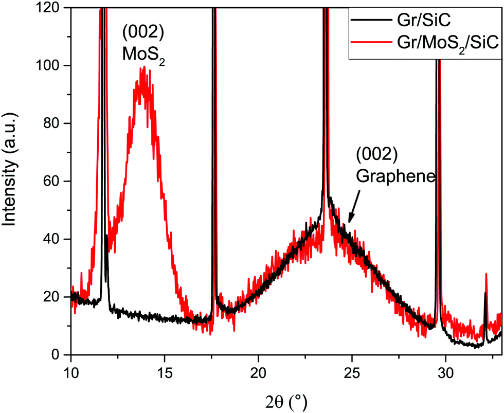 | ||
| Fig. 2 ω-2θ scan of the sample Gr/MoS2/SiC showing well developed MoS2 and graphene peaks. Same scan for the Gr/SiC substrate showing a similar graphene peak. The position and FWHM of the graphene peak before and after Mo evaporation are almost the same. | ||
Additionally a ω-scan, with a fixed position of the X-ray detector on the 2 scale, was also employed to verify the quality and positioning of the MoS2 layer with respect to the underlying SiC substrate (Fig. 3). The ω-scan of the Gr/MoS2/SiC sample was taken for a fixed position of the X-ray detector corresponding to the 002 reflection from a MoS2 type structure. The sample itself was set to reflect from crystallographic planes which are parallel to the sample substrate SiC. The measurements were taken along the direction of main atomic surface steps of the 6H-SiC. The FWHM of the ω scan peak is at the level of 0.06°, which means that the MoS2 layer is highly oriented. We can conclude that the quality of the MoS2 layer, confirmed by the FWHM of the peak for the ω-scan and very good alignment with the SiC surface, is at very high level.
 | ||
| Fig. 3 ω-Scan for the Gr/MoS2/SiC sample indicating a high quality of the MoS2 layer with FWHM = 0.06°. | ||
This is indeed very surprising as growing MoS2 layers with the same technique on other substrates has led to a polycrystalline material. To provide a suitable explanation it is necessary to study the intercalation process in more detail. For practical reasons a sample with Mo evaporated on top of the graphene layer has been chosen for this purpose. The SIMS tool allows one to heat a sample holder in the load lock and thus it is possible to study the evolution of the intercalation process as a function of the thermal treatment without removing the sample from a vacuum environment. The sample has been annealed at 250 °C for fifteen minutes and transferred to the measurement chamber for the SIMS analysis. This time, however, a lateral imaging mode has been used to study the spatial distribution of Mo at the surface of the sample and close to the SiC substrate (Fig. 4(a) and (b), respectively). It becomes immediately apparent that the intercalation process indeed occurs at the step edges of the sample: both molybdenum depletion at the surface and agglomeration close to the substrate are directly related to the position of the edges.
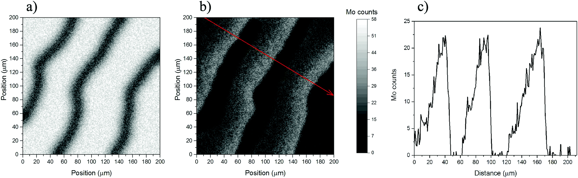 | ||
| Fig. 4 SIMS lateral imaging showing the distribution of Mo after evaporation and annealing at 250 °C. (a) At the surface of the sample. (b) Close to the SiC substrate. (c) A profile of Mo counts along the red arrow presented in part (b). | ||
There is, however, a significant difference between these two pictures: while the depletion of Mo at the surface is symmetrical the agglomeration and diffusion close to the SiC substrate are clearly occurring only in one direction. It is even better visible in Fig. 4(c), which presents a profile of Mo counts along the red arrow presented in part (b). These results further indicate that the intercalation most likely occurs at the bottom of the step edges of the SiC substrate and thus molybdenum atoms diffuse along the terrace but cannot overcome the barrier of the step. However, it is possible that some textured structure is formed when molybdeum disulfide layers from different terraces are merged together forming a highly oriented but not necessary continuous layer.
4 Conclusions
Complementary use of several advanced characterization techniques has revealed that an attempt to grow MoS2 layers on a Gr/SiC substrate results in formation of a Gr/MoS2/SiC heterostructure. The process of intercalation of molybdenum and sulphur atoms under the graphene layer clearly leads to creation of well organized MoS2 layers. We suggest that the intercalation process takes place almost exclusively via the step edges of the SiC substrate and is most probably related to graphene defects present there. Mo and S atoms can only diffuse along the SiC terrace underneath the more perfect graphene plane and thus a single crystallization front ensures high quality and orientation of the MoS2 layer. These findings may be of the utmost importance for fabrication of future electronic devices based on 2D material heterostructures.Conflicts of interest
There are no conflicts to declare.Acknowledgements
This work was supported by the European Union's Horizon 2020 research and innovation programme under grant agreement No 785219. The first author was supported by the National Science Centre within the SONATA14 2018/31/D/ST5/00399 project.References
- S. Ding, D. Zhang, J. S. Chen and X. W. D. Lou, Nanoscale, 2012, 4, 95–98 RSC.
- Y. Li, H. Wang, L. Xie, Y. Liang, G. Hong and H. Dai, J. Am. Chem. Soc., 2011, 133, 7296–7299 CrossRef CAS.
- S. Wi, H. Kim, M. Chen, H. Nam, L. J. Guo, E. Meyhofer and X. Liang, ACS Nano, 2014, 8, 5270–5281 CrossRef CAS PubMed.
- A. K. Geim and I. V. Grigorieva, Nature, 2013, 499, 419–425 CrossRef CAS.
- M. Chhowalla, H. S. Shin, G. Eda, L.-J. Li, K. P. Loh and H. Zhang, Nat. Chem., 2013, 5, 263–275 CrossRef.
- W. Wu, L. Wang, Y. Li, F. Zhang, L. Lin, S. Niu, D. Chenet, X. Zhang, Y. Hao, T. F. Heinz, J. Hone and Z. L. Wang, Nature, 2014, 514, 470–474 CrossRef CAS.
- R. Ganatra and Q. Zhang, ACS Nano, 2014, 8, 4074–4099 CrossRef CAS.
- X. Li and H. Zhu, J. Materiomics, 2015, 1, 33–44 CrossRef.
- Z. Wang, H.-H. Wu, Q. Li, F. Besenbacher, X. C. Zeng and M. Dong, Nanoscale, 2018, 10, 18178–18185 RSC.
- S. Kim, A. Konar, W.-S. Hwang, J. H. Lee, J. Lee, J. Yang, C. Jung, H. Kim, J.-B. Yoo, J.-Y. Choi, Y. W. Jin, S. Y. Lee, D. Jena, W. Choi and K. Kim, Nat. Commun., 2012, 3, 1011 CrossRef.
- P. Zhang, Z. Wang, L. Liu, L. H. Klausen, Y. Wang, J. Mi and M. Dong, Appl. Mater. Today, 2019, 14, 151–158 CrossRef.
- A. Gurarslan, Y. Yu, L. Su, Y. Yu, F. Suarez, S. Yao, Y. Zhu, M. Ozturk, Y. Zhang and L. Cao, ACS Nano, 2014, 8, 11522–11528 CrossRef CAS.
- X. Wang, H. Feng, Y. Wu and L. Jiao, J. Am. Chem. Soc., 2013, 135, 5304–5307 CrossRef CAS.
- Y.-H. Lee, X.-Q. Zhang, W. Zhang, M.-T. Chang, C.-T. Lin, K.-D. Chang, Y.-C. Yu, J. T.-W. Wang, C.-S. Chang, L.-J. Li and T.-W. Lin, Adv. Mater., 2012, 24, 2320–2325 CrossRef CAS.
- Y. Zhan, Z. Liu, S. Najmaei, P. M. Ajayan and J. Lou, Small, 2012, 8, 966–971 CrossRef CAS.
- Y. Lee, J. Lee, H. Bark, I.-K. Oh, G. H. Ryu, Z. Lee, H. Kim, J. H. Cho, J.-H. Ahn and C. Lee, Nanoscale, 2014, 6, 2821–2826 RSC.
- Y. Shi, W. Zhou, A.-Y. Lu, W. Fang, Y.-H. Lee, A. L. Hsu, S. M. Kim, K. K. Kim, H. Y. Yang, L.-J. Li, J.-C. Idrobo and J. Kong, Nano Lett., 2012, 12, 2784–2791 CrossRef CAS.
- J. Jeon, S. K. Jang, S. M. Jeon, G. Yoo, Y. H. Jang, J.-H. Park and S. Lee, Nanoscale, 2015, 7, 1688–1695 RSC.
- M. H. Heyne, D. Chiappe, J. Meersschaut, T. Nuytten, T. Conard, H. Bender, C. Huyghebaert, I. P. Radu, M. Caymax, J.-F. de Marneffe, E. C. Neyts and S. De Gendt, J. Mater. Chem. C, 2016, 4, 1295–1304 RSC.
- A. Stesmans, S. Iacovo, D. Chiappe, I. Radu, C. Huyghebaert, S. De Gendt and V. V. Afanas'ev, Nanoscale Res. Lett., 2017, 12, 283 CrossRef CAS.
- K. Lee, R. Gatensby, N. McEvoy, T. Hallam and G. S. Duesberg, Adv. Mater., 2013, 25, 6699–6702 CrossRef CAS.
- P. P. Michałowski, P. Knyps, P. Ciepielewski, P. Caban, E. Dumiszewska and J. Baranowski, Phys. Chem. Chem. Phys., 2019, 21, 8837–8842 RSC.
- K. S. Novoselov, A. Mishchenko, A. Carvalho and A. H. Castro Neto, Science, 2016, 353, aac9439 CrossRef CAS.
- W. Strupinski, K. Grodecki, A. Wysmolek, R. Stepniewski, T. Szkopek, P. E. Gaskell, A. Grüneis, D. Haberer, R. Bozek, J. Krupka and J. M. Baranowski, Nano Lett., 2011, 11, 1786–1791 CrossRef CAS.
- K. V. Emtsev, F. Speck, T. Seyller, L. Ley and J. D. Riley, Phys. Rev. B: Condens. Matter Mater. Phys., 2008, 77, 155303 CrossRef.
- W. Strupinski, K. Grodecki, P. Caban, P. Ciepielewski, I. Jozwik-Biala and J. Baranowski, Carbon, 2015, 81, 63–72 CrossRef CAS.
- C. Riedl, C. Coletti, T. Iwasaki, A. A. Zakharov and U. Starke, Phys. Rev. Lett., 2009, 103, 246804 CrossRef CAS.
- M. Tokarczyk, G. Kowalski, M. Możdżonek, J. Borysiuk, R. Stepniewski, W. Strupiński, P. Ciepielewski and J. M. Baranowski, Appl. Phys. Lett., 2013, 103, 241915 CrossRef.
- T. Gao, Y. Gao, C. Chang, Y. Chen, M. Liu, S. Xie, K. He, X. Ma, Y. Zhang and Z. Liu, ACS Nano, 2012, 6, 6562–6568 CrossRef CAS.
- M. U. Kahaly, T. Kaloni and U. Schwingenschlögl, Chem. Phys. Lett., 2013, 578, 81–84 CrossRef.
- R. Honig, P. Roese, K. Shamout, U. Berges and C. Westphal, Nanotechnology, 2019, 30, 025702 CrossRef CAS.
- I. Gierz, T. Suzuki, R. T. Weitz, D. S. Lee, B. Krauss, C. Riedl, U. Starke, H. Höchst, J. H. Smet, C. R. Ast and K. Kern, Phys. Rev. B: Condens. Matter Mater. Phys., 2010, 81, 235408 CrossRef.
- K. V. Emtsev, A. A. Zakharov, C. Coletti, S. Forti and U. Starke, Phys. Rev. B: Condens. Matter Mater. Phys., 2011, 84, 125423 CrossRef.
- K. Li, X. Feng, W. Zhang, Y. Ou, L. Chen, K. He, L.-L. Wang, L. Guo, G. Liu, Q.-K. Xue and X. Ma, Appl. Phys. Lett., 2013, 103, 062601 CrossRef.
- W. Norimatsu and M. Kusunoki, Phys. E, 2010, 42, 691–694 CrossRef CAS.
- O. V. Yazyev and S. G. Louie, Nat. Mater., 2010, 9, 806 CrossRef CAS.
- CAMECA, Genneviliers, CAMECA SC-Ultra, User's Guide, 2005.
- D. Kouzminov, A. Merkulov, E. Arevalo and H. J. Grossmann, Surf. Interface Anal., 2013, 45, 345–347 CrossRef CAS.
- A. Merkulov, Surf. Interface Anal., 2013, 45, 90–92 CrossRef CAS.
- C. A. Andersen and J. R. Hinthorne, Science, 1972, 175, 853–860 CrossRef CAS PubMed.
- A. Benninghoven, Surf. Sci., 1975, 53, 596–625 CrossRef CAS.
- A. Benninghoven, F. G. Rudenauer and H. W. Werner, Secondary ion mass spectrometry: basic concepts, instrumental aspects, applications and trends, John Wiley & Sons, New York, 1987 Search PubMed.
- H. W. Werner, Surf. Sci., 1975, 47, 301–323 CrossRef CAS.
- H. Liebl, J. Vac. Sci. Technol., A, 1975, 12, 385 CrossRef CAS.
- H. Liebl, J. Appl. Phys., 1967, 38, 5277–5283 CrossRef CAS.
- P. P. Michałowski, W. Kaszub, A. Merkulov and W. Strupiński, Appl. Phys. Lett., 2016, 109, 011904 CrossRef.
- P. P. Michałowski, W. Kaszub, I. Pasternak and W. Strupinski, Sci. Rep., 2017, 7, 7479 CrossRef.
- P. P. Michałowski, I. Pasternak and W. Strupinski, Nanotechnology, 2018, 29, 015702 CrossRef.
- I. Grzonka, J. Pasternak, P. P. Michałowski, V. Kolkovsky and W. Strupinski, Appl. Surf. Sci., 2018, 447, 582–586 CrossRef.
- P. P. Michałowski, I. Pasternak, P. Ciepielewski, F. Guinea and W. Strupinski, Nanotechnology, 2018, 29, 305302 CrossRef PubMed.
- P. Caban, D. Teklińska, P. Michałowski, J. Gaca, M. Wójcik, J. Grzonka, P. Ciepielewski, M. Możdżonek and J. Baranowski, J. Cryst. Growth, 2018, 498, 71–76 CrossRef CAS.
- P. P. Michałowski, P. Caban and J. Baranowski, J. Anal. At. Spectrom., 2019, 34, 848–853 RSC.
| This journal is © the Owner Societies 2019 |