
Computational acceleration of prospective dopant discovery in cuprous iodide†
Miglė
Graužinytė
 a,
Silvana
Botti‡
b,
Miguel A. L.
Marques‡
c,
Stefan
Goedecker
a and
José A.
Flores-Livas
*ad
a,
Silvana
Botti‡
b,
Miguel A. L.
Marques‡
c,
Stefan
Goedecker
a and
José A.
Flores-Livas
*ad
aDepartment of Physics, Universität Basel, Klingelbergstr. 82, 4056 Basel, Switzerland. E-mail: jose.flores@unibas.ch; Tel: +41 61 207 3738
bInstitut für Festkörpertheorie und -optik, Friedrich-Schiller-Universität Jena, Max-Wien-Platz 1, 07743 Jena, Germany
cInstitut für Physik, Martin-Luther-Universität Halle-Wittenberg, D-06099 Halle, Germany
dDipartimento di Fisica, Università di Roma La Sapienza, Piazzale Aldo Moro 5, I-00185 Roma, Italy
First published on 22nd July 2019
Abstract
The zinc blende (γ) phase of copper iodide holds the record hole conductivity for intrinsic transparent p-type semiconductors. In this work, we employ a high-throughput approach to systematically explore strategies for enhancing γ-CuI further by impurity incorporation. Our objectives are not only to find a practical approach to increase the hole conductivity in CuI thin films, but also to explore the possibility for ambivalent doping. In total 64 chemical elements were investigated as possible substitutionals on either the copper or the iodine site. All chalcogen elements were found to display acceptor character when substituting iodine, with sulfur and selenium significantly enhancing carrier concentrations produced by the native VCu defects under conditions most favorable for impurity incorporation. Furthermore, eight impurities suitable for n-type doping were discovered. Unfortunately, our work also reveals that donor doping is hindered by compensating native defects, making ambipolar doping unlikely. Finally, we investigated how the presence of impurities influences the optical properties. In the majority of the interesting cases, we found no deep states in the band-gap, showing that CuI remains transparent upon doping.
1 Introduction
In the near future, transparent electronic and photonic devices will become an integral part of our lives, with transparent solar panels turning windows into power generators. The key to this technological advancement lies in materials that are transparent to visible light, yet able to carry an electric current. The so-called transparent conductive materials (TCMs) are usually large band gap semiconductors heavily doped with electrons (n-type) or holes (p-type).During the last few decades, significant advances have been made in the development of n-type transparent conductors, mainly indium tin oxide (ITO), but also doped SnO2, ZnO2, and GaN.1–3 Among the known n-type TCMs, ITO has the highest conductivity (σ = 104 Ω−1 cm−1) coupled with a transparency in the visible range of 80–90%.1 On the other hand, good p-type TCMs remain elusive despite the many candidate materials that have been investigated both experimentally and theoretically (see, e.g., the review by Banerjee and Chattopadhyay4), since the first report of a p-type transparent conductor obtained using NiO.5
Nickel oxides represent the first class of potentially interesting materials due to their high work function favouring p-type doping. In fact, effective doping is key to transforming an insulator into a transparent conductor.6 In this context, a high work function favours p-type conductivity by preventing the anion vacancy from being electrically active. In ZnO, for example, the rather low ionization level and formation energy of oxygen vacancies impede high p-type doping under thermodynamic equilibrium.7
At the end of the 1990s a new family of promising p-type TCMs was identified among the Cu (Ag and Au) oxides with the delafossite structure.8 In these oxides, the p–d repulsion pushes the valence band maximum upwards favoring a high work function. Hole conductivity was first reported for the delafossite CuAlO2 in 1997,9 and since then several other delafossites have been investigated.10–17 However, all delafossite TCMs present conductivities at least one to two orders of magnitude lower than their n-type counterparts. The best delafossite proposed to date is CuCr1−xMgxO2, exhibiting σ = 220 Ω−1 cm−1, a Hall mobility of approximately 1 cm2 V−1 s−1,18 but poor transparency (less than 30%) in the visible range. Delafossites display highly complex electronic structures14,15 and the associated mechanism for hole conduction is still not completely understood.
It is clear that a solution for the lack of high-performance p-type transparent semiconductors and the discovery of bipolar transparent components represent essential milestones for embedding electronics into transparent systems. In this respect, cuprous iodide (CuI) has recently emerged as one of the most promising candidates for p-type transparent conductors.19 This unique large band gap semiconductor was already shown to possess a record high p-type conductivity and simultaneous transparency, resulting in a factor of 100 improvement in the figure of merit, when compared to any other p-type TCM.20 In fact, CuI demonstrates optical transparency values as high as 90%21 and hole concentrations in the range of 4.0 × 10¹⁶–8.6 × 1019 cm−3, with mobilities of 2–43.9 cm2 V−1 s−1.19,21 The carrier masses of 0.30(1)me are reported experimentally for electrons22 and are calculated to be 0.2–0.25me for light holes23 (heavy holes display masses of 2.4(3)me22). The band gap of 3.1 eV has been reported for CuI at T = 80 K,24 but room temperature experimental studies suggest a somewhat lower value of 2.93–3.03 eV.25–29 Consequently, applications of cuprous iodide in organic electronics, solar cells, and bipolar diodes, as well as thermoelectricity have been proposed19 and transparent p–n junctions using CuI have been synthesized.30
Despite these recent spectacular results, to enable technological applications charge carrier concentrations need to be increased further, while preserving hole mobilities and transparency at the same time. Moreover, a deep understanding of electronic excitation, charge transport mechanisms and defect physics of CuI is far from being achieved and further theoretical studies are essential to guide experiments in order to reach beyond the present performance. As such, we present here an exhaustive theoretical study of substitutional doping in γ-CuI – the low temperature (below 660 K) and ambient pressure phase of CuI, that crystallizes into a zinc blende (F![[4 with combining macron]](https://www.rsc.org/images/entities/char_0034_0304.gif) 3m) structure,31,32 see the left panel of Fig. 1. We investigate substitutions of both the Cu-site and the I-site using 64 candidate chemical elements. This includes all elements of the periodic table up to radium, excluding only lanthanides, actinides, rare gases, and astatine. We are searching not only for hole dopants, that might be used to increase the carrier concentration of p-type CuI, but also for n-type elements to explore the possibility of ambipolar doping in this material.
3m) structure,31,32 see the left panel of Fig. 1. We investigate substitutions of both the Cu-site and the I-site using 64 candidate chemical elements. This includes all elements of the periodic table up to radium, excluding only lanthanides, actinides, rare gases, and astatine. We are searching not only for hole dopants, that might be used to increase the carrier concentration of p-type CuI, but also for n-type elements to explore the possibility of ambipolar doping in this material.
 | ||
| Fig. 1 Atomic and electronic structure of γ-CuI. Left: Atomic structure of the 64 atom CuI supercell used in calculations. The different defect sites are indicated by bright blue spheres, copper atoms are shown in light green, and iodine atoms in red. Right: Electronic band structure (calculated using PBE0) along selected high-symmetry directions and the corresponding partial density of states. Red points around Γ indicate the shift in energy due to spin–orbit coupling contribution. The resultant change in the band gap is also indicated. | ||
2 Results and discussion
2.1 Bulk CuI
A suitable exchange–correlation functional for studying defects in γ-CuI was determined by comparing the calculated properties of bulk cuprous iodide with the available experimental data. We tested one semi-local functional, specifically the Perdew–Burke–Ernzerhof (PBE) approximation,33 and two hybrid-functionals popular for solid-state calculations, namely the one-parameter hybrid PBE034,35 and the screened hybrid HSE06.36,37 The results for the lattice constant (a), bulk modulus (B0), heat of formation (ΔEF), and the electronic band gap (EG) are summarized in Table 1.All three functionals were able to reproduce the cubic lattice constant of the crystalline phase with an accuracy better than 1%. The low bulk modulus of cuprous iodide was also captured well by both local and hybrid functionals, with HSE06 showing the best agreement between experiment and theory. Unfortunately, as is typical of local exchange–correlation functionals41 the electronic band gap was strongly (almost 60%) underestimated by PBE. This functional also resulted in a heat of formation that is significantly smaller than that measured experimentally. An improved performance was seen with HSE06, resulting in a significantly more accurate heat of formation value but leading to a band gap that is, nevertheless, 0.5 eV too small. In contrast, the PBE0 electronic gap has a value of 3.2 eV, very close to the experimentally measured 3.0–3.1 eV25–28 and a formation energy that is in agreement with experiment. Since an accurate description of the electronic band gap is crucial for determining defect formation energies, we selected PBE0 as the most appropriate functional for studying defects in cuprous iodide.
Finally, the dependence of the band gap on spin–orbit interactions was investigated using the chosen PBE0 functional. Such interactions have been previously reported to induce significant contributions in copper halide compounds.42,43 The shift in the electronic bands of CuI due to spin–orbit coupling around the direct band gap at Γ is indicated via red points in Fig. 1. We see a small reduction of the band gap of 0.23 eV, bringing our estimated band gap closer to the values typically measured for CuI thin-films. For comparison, a value of 0.64 eV has been reported experimentally for the spin–orbit splitting in CuI.43 In the right most panel of Fig. 1 we show the partial density of states for orbitals contributing most to the conduction and valence band edges. It is evident that the valence band maximum (VBM), made up of I-5p and Cu-3d hybridized states, results in a stronger spin–orbit interaction effect, while the conduction band minimum (CBM), owing its disperse character to the s-orbitals of both elements, is largely unaffected.
2.2 Screening methodology
The formation energy of a given defect, Dx, contains crucial information about the stability of different charge states available to this defect. For an impurity element to act as a successful dopant it should be stable in a charge-donating state. If hole conduction is desired, a good dopant element should release one or more holes into the valence band. This is achieved if the impurity remains stable in a negative charge state as the Fermi level approaches the valence band (shallow acceptor). On the other hand, for electron conduction, the dopant should release one or more electrons into the conduction band. In this case, the impurity element should be stable in a positive charge state for Fermi levels close to the conduction band (shallow donor).For optoelectronic applications, however, the successful release of charge-carriers is a necessary but not sufficient condition to achieve useful doping. Indeed, not only good conductivity is required, but also optical transparency in the visible range. For full transparency this translates to an optical band gap larger than around 3 eV (although absorption in the infrared is allowed), and this property should not be modified by the impurity defects. This can be inferred from the electronic band structure or the density of states (DOS). All impurities creating deep electronic defect-states are likely to result in parasitic absorption, affecting negatively the optical properties of the host. Furthermore, deep defect states are often linked to charge trapping centers.44 A band gap free of deep defect states is, therefore, a good indicator of a promising dopant element.
As a consequence, we used two properties to determine the suitability of a given dopant element, specifically the electronic DOS and the formation energy,  , as a function of the charge state, q, and the Fermi level, εF. The energy required to ionize the defect can then be obtained by evaluating the corresponding thermodynamic transition level, ε(q1/q2), using
 | (1) |
 | (2) |
 is the energy of a supercell with a defect atom D in a charge state q placed at a given site x and ECuI is the energy of the host (γ-CuI) supercell without the defect. Furthermore, ni is the number of atoms of type i that were put in (ni > 0) or taken out (ni < 0) of the supercell in order to create the defect. For example, a copper vacancy, VCu, corresponds to nCu = −1, while a carbon atom in an iodine site, CI, leads to nI = −1 and nC = +1.
The chemical potential of each species i, μi, is referenced to the elemental phase, and we determine the interval of possible values of Δμi by considering secondary phase formation (further information on the reference phases can be found in the ESI†). The flexibility in choosing the values of Δμi provides a link to the experimental conditions: a Cu-rich environment corresponds to ΔμCu = 0, while Cu-poor (I-rich) conditions imply ΔμI = 0. Finally, ΔεF is the position of the Fermi level with respect to the energy of the valence band maximum, εVBM, in the stoichiometric CuI. Similarly to the chemical potentials, the value of ΔεF can be considered as a parameter reflecting experimental conditions. Values of ΔεF close to the conduction band indicate an n-type material, and those close to the valence band indicate a p-type material. Finally, additional correction terms arising from the use of the supercell approach are gathered in Ecor. These include a band-filling correction for the hybrid-functional calculations and corrections for charged interactions and potential alignment for all charged defect calculations.45
For each impurity species, D, the copper site, DCu, and the iodine site, DI, were tested. The two sites are indicated in the left panel of Fig. 1. The elements identified as good substitutional dopants in the first step were tested further by considering two additional incorporation sites: the interstitial site amongst iodine atoms, Ditet-I, shown as a red tetrahedron in the left panel of Fig. 1, and the interstitial site amongst copper atoms, Ditet-Cu, shown as a green tetrahedron.
To evaluate efficiently the formation energies of all 64 candidate elements considered in this study, we performed a pre-screening step using the PBE semi-local exchange–correlation functional, following the approach in ref. 46. Such a step has been shown to be highly effective in dopant searches in other TCMs.46,47 In this way very unstable substitutions and deep defects can be easily eliminated. Most importantly, the tendency of semi-local functionals to delocalize charges will always predict impurity defects to be shallower, thus, allowing us to retain all elements of potential interest. Consequently, expensive hybrid-functional calculations need to be performed only for a small subset of impurities.
2.3 p-Type dopants
We summarize, in Fig. 2, the results of our search for potential acceptor dopants, from the initial screening step using the PBE functional. The energetically stable substitutional site of each element is indicated by the geometric shapes: a triangle corresponds to preferred copper substitution, while a rectangle to a favored iodine substitution. The color of the geometric shape denotes the stable charge state of this substitution under p-type conditions, i.e. when ΔεF = 0. A suitable acceptor dopant should be stable in a negative charge state (indicated by a blue color) under these conditions. It is immediately evident from Fig. 2 that none of the impurity substitutions favor this charge state when the Fermi level is at the VBM. This indicates that no impurity dopants are able to induce degenerate hole conduction in cuprous iodide. In our study, only the elements of the chalcogen series were identified as relatively shallow acceptors, displaying thermodynamic transition levels to a hole generating (q = −1) charge state within 300 meV from the valence band edge. These elements are highlighted by a blue outline in Fig. 2. | ||
| Fig. 2 PBE pre-screening results for ΔεF at the valence band maximum and under I-rich conditions. Geometric shapes indicate the energetically favored substitution: DCu marked by a triangle, and DI by a rectangle. The color of the shape indicates the stable charge state: blue < 0, yellow 0, orange > 1. The bottom right corner of each element panel denotes the energy difference (in eV) between the two sites. The stable charge state of the unstable site is shown by the color of the small circle. Outlined in blue are potential p-type dopants. | ||
A chalcogen impurity releases a hole only when replacing an iodine, but not when substituting a copper. Consequently, the energetic competition between the two substitutional sites is relevant for determining the suitability of these dopants. The PBE energy difference between the stable charge states of the different substitutional sites is indicated by the number at the bottom right of each element's panel in Fig. 2. In this way, we can verify that a significant preference for the electrically active iodine site is displayed by all chalcogen impurities, with the smallest energy difference of 1.5 eV found for polonium. Such a large difference suggests that Cu-site chalcogen substitutionals are negligible at room temperature.
Besides the chalcogens, only halogens, carbon and some of the group V-A elements prefer the iodine site. Even fluorine displays similar formation energies for the two positions, despite being isovalent to iodine. The stable charge state of the less favored substitutional site is shown by the color of the small circles in Fig. 2. It can, therefore, be seen that impurity incorporation is not expected to result in shallow hole generation even if the alternative substitutional positions were stabilized. As a result, potential acceptor dopants in CuI are limited to a handful of chalcogen impurities.
For chalcogens, we double checked the stability of the iodine site by investigating the possibility of the formation of interstitials. We considered two interstitial sites that are indicated by colored tetrahedrons in the left panel of Fig. 1. All chalcogens showed preference for the copper coordinated tetrahedron (over the iodine coordinated one), favoring a neutral charge state in this position at a Fermi level reflecting a p-type material. Nevertheless, interstitial incorporation remains highly unlikely when compared to iodine substitution, with the lowest energetic difference observed for polonium at a hefty 5.2 eV.
We recalculated defect formation energies for the most promising acceptor substitutionals using the more accurate PBE0 hybrid functional (PBE0). The results, under Cu-rich (I-poor) growth conditions, are summarized in panel (a) of Fig. 3. These are the most suitable conditions for iodine-substitutional defects to form, as they favor the formation of iodine vacancies, VI. For comparison, the formation energy of the copper vacancy, considered to be responsible for the intrinsic p-type conductivity in CuI,19,23,48,49 was also included in the plot. We found that the VCu defect has a thermodynamic transition ε(0/−) level at 280 meV above the valence band edge in our PBE0 calculations. This value is in reasonable agreement with a preceding defect study,23 reporting ε(0/−) transitions at 180 meV for PBE and 210 meV for PBE+U. However, our result is significantly higher than an alternative PBE study that found a value of 44 meV48 and an HSE06 study reporting 23 meV.49 Interestingly, all our native defect PBE results show good agreement with the corresponding PBE results from ref. 23, but not ref. 48, where only VI out of the six intrinsic defects considered has a reasonable energetic match. We were unable to identify the origin of these large discrepancies.
 | ||
| Fig. 3 Left panel: PBE0 formation energies of potential p-type dopants, as well as the native VCu (dotted-line), evaluated under Cu-rich conditions. Only the stable charge states are shown. The black arrow indicates the self-consistent Fermi-level calculated with SI doping. Right panel: Thermal equilibrium charged defect concentrations as a function of temperature, calculated based on the formation energies shown in the left panel. | ||
Unlike the native VCu defect, all impurity acceptors display a direct ε(+/−) thermodynamic transition. The lowest transition level is that of oxygen at 145 meV and the highest level of polonium at 440 meV, reflecting the decreasing electronegativity of the elements along the series. Both the relatively deep ionization energies of the chalcogen impurities and their self-compensating nature (due to a direct ε(+/−) transition) make these elements not ideal for enhancing the p-type nature of cuprous iodide. Nevertheless, as Fig. 3 reveals, oxygen and sulfur display lower and selenium comparable ionization levels to the intrinsic copper vacancy. Furthermore, the absolute formation energies of SI and SeI lie almost 1 eV lower in energy than VCu under Cu-rich conditions, suggesting that the number of free-carriers could still be enhanced by introducing these elements.
To support this claim, we calculated the concentrations of each impurity defect in thermodynamic equilibrium as a function of temperature T. The Fermi level at a given T was evaluated using a self-consistent approach described in detail in the Appendix. The estimate of the Fermi level that we obtained was then used to determine defect concentrations based on Boltzmann statistics. Six native defects (VCu, VI, ICu, CuI, Iint, and Cuint) were used together with the substitutional defect to approximate charge neutrality in the material. Formation energies as a function of the Fermi level for the native defects used can be found in Fig. 7 in the Appendix.
Calculated impurity defect concentrations are summarized in the right panel of Fig. 3. The estimated Fermi level in the presence of sulfur (the most promising dopant) is indicated by a black arrow in the left panel. In the entire 250–650 K temperature range, the Fermi level is pinned at approximately 220 meV above the valence band. This value is significantly lower than the 550 meV calculated for undoped CuI films under the same conditions and comparable to the 170 meV level obtained for undoped CuI films under I-rich conditions (see Appendix). The latter case strongly favors the formation of copper vacancies, but hampers the substitution of iodine. In accordance with the Fermi level values, the right panel of Fig. 3 reveals a significant increase in acceptor defects with the introduction of both sulfur and selenium. Tellurium donates an almost identical concentration of holes to VCu, while low defect incorporation is anticipated for both oxygen and polonium at room temperature. The corresponding concentrations of defects under I-rich conditions can be found in the ESI.†
Even though only SI and SeI are seen to enhance the concentrations of acceptor charge carriers in thermodynamic equilibrium, impurity doping offers an additional advantage over intrinsic defect creation: it is easier to incorporate large (off-equilibrium) concentrations of impurity defects into films during the deposition process. The resultant point defects may then be stabilized by the large activation energies required to diffuse out of the bulk. As a consequence, enhancement in carrier concentrations under Cu-rich conditions may be expected with incorporation of the other chalcogen impurities as well.
2.4 n-Type dopants
We also address the possibility of ambipolar doping in cuprous iodide. The initial PBE pre-screening data are summarized in Fig. 4, with the stable substitutional site under n-type conditions, i.e. when ΔεF is at the CBM, indicated using geometrical shapes. Due to the different behavior of oppositely charged defect states with increasing Fermi level, three different elements – boron, silicon and germanium – yield the lowest energy on the I-site (when the Fermi level is at the CBM) or the Cu-site (Fermi level at the VBM). Therefore, Cu-rich conditions, which favor the formation of iodine substitutionals, are depicted in Fig. 4. Since most n-type dopants seem to favor the Cu-site, these conditions ensure that elements where the competition between the two sites is close are excluded. For example, in the case of germanium, the compensating I-site substitution with its acceptor character is likely to undermine donor doping efforts.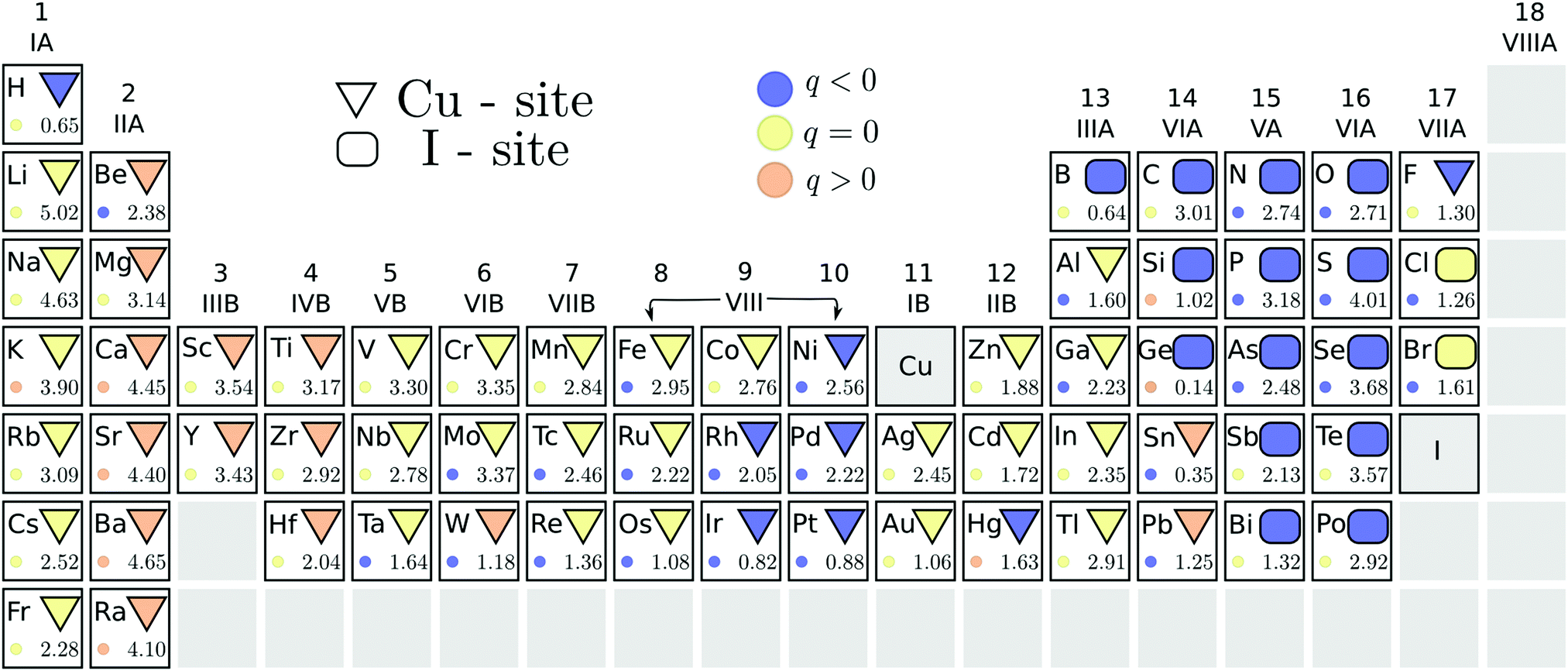 | ||
| Fig. 4 PBE pre-screening results for ΔεF at the conduction band minimum and under Cu-rich conditions. Geometric shapes indicate the energetically favored substitution: DCu marked by a triangle and DI by a rectangle. The color of the shape indicates the stable charge state: blue < 0, yellow 0, and orange > 1. The bottom right corner of each element panel denotes the energy difference (in eV) between the two sites. The stable charge state of the unstable site is shown by the color of the small circle. All elements with an orange geometric shape are potential n-type dopants. | ||
The stable charge state of each defect in the energetically favored position is denoted by the color of the geometric shape. In contrast to acceptors, multiple impurity substitutions retain a positive (donor) charge state when the Fermi level is at the conduction band edge. Among these elements, marked by orange colored geometric shapes in Fig. 4, are the alkaline-earth metals, group III- and IV-B transition metals, tungsten and most of the group VI-A elements (if incorporated on the Cu-site). However, from the latter group only Sn and Pb favor replacing copper instead of iodine. The energetic difference between the two substitutional sites is indicated by the number at the bottom of each element's panel in Fig. 4. We are, thus, able to identify tin as the most likely amongst the donor elements to incorporate on the alternative site, followed by tungsten and lead that already display a significant (≈1.2 eV) energy difference between the two positions.
The stable charge states corresponding to the less favored substitutions, indicated by colored circles in Fig. 4, show that not only Si and Ge, but also mercury and potassium could act as donors on the less favored iodine substitutional site. However, the formation energies of these positions are simply too high for significant incorporation to be achieved. The same observation is true for the heavier alkaline-earth metals that are predicted to act as donors regardless of the substitutional position taken.
Within the stable n-type dopant candidates, both scandium and yttrium induce electronic defect states below the conduction band edge. Such states are likely to be detrimental to the optical properties of the transparent conductor. The same behavior was also identified for Ti, Zr, Hf, and W impurities, which further display spin polarization and corresponding magnetic behavior. Based on the introduction of the detrimental defect states, these elements were excluded from further steps in our search for useful donor substitutionals for transparent conductor applications.
For the remaining eight donor impurities, we investigated the possibility of interstitial incorporation. We found that all donor impurities investigated retained their n-type character even when placed on the interstitial site, thus promoting electron generation regardless of the location. Furthermore, analogous to the p-type defects, interstitial positions were found to be significantly less favorable. Interestingly, all of the n-type impurities preferred the Cu-coordinated tetrahedral site to the I-coordinated one, despite favoring copper substitution in the bulk lattice.
We calculated defect formation energies for the eight promising donor impurities using PBE0. The results, under Cu-rich (I-poor) growth conditions, are summarized in the left panel of Fig. 5. We again compare our results with the most prominent native defects of the same character: the iodine vacancy VI (dotted-black-line), and the copper interstitial Cuint (dashed-gray-line). The anion vacancy is anticipated to act as the dominant intrinsic donor. This has indeed been predicted in previous works using both the PBE and HSE06 exchange–correlation functionals.23,48 However, we discover that VI displays an amphoteric character, i.e. the defect opposes the main charge carriers under both n- and p-type conditions. We suspect that the deep ε(+/−) transition was overlooked in previous works, simply because the negative charge state of the vacancy was not considered. For Cuint a deep ε(+/0) transition is observed at almost 1 eV below the CBM using PBE0. Thus, no native defects are expected to generate significant electron concentrations in γ-CuI, lending an insight into why acceptor charge carriers are dominant in the undoped material.
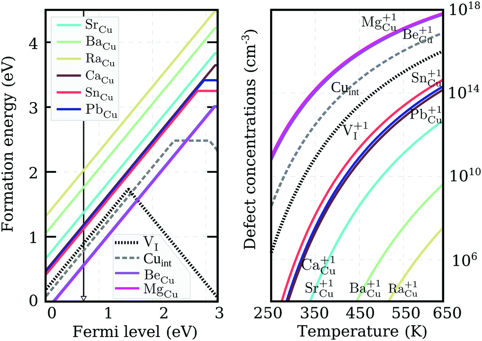 | ||
| Fig. 5 Left panel: PBE0 formation energies for the potential n-type dopants in CuI, and two native defects, VI (dotted-line) and Cuint (dashed-line), under Cu-rich conditions. The black arrow indicates the self-consistent Fermi-level calculated with BeCu doping. Right panel: Thermal equilibrium charged defect concentrations as a function of temperature, calculated based on the formation energies shown in the left panel. | ||
Interestingly, neither charged configuration (q = 1 and q = −1) of the iodine vacancy introduces deep electronic defect states, maintaining the optical transparency of CuI. However, for charge neutral VI a spin polarized electronic structure with a peak at 1.89 eV above the VBM is predicted. A similar peak at 680 nm (or 1.82 eV) linked to the formation of iodine vacancies has indeed been observed in photo-conductivity spectra upon high temperature annealing.28 Moreover, the peak is suppressed when annealing in the presence of iodine50 further confirming its VI origin. However, the high temperatures (at and above 430 °C) reported by Gruzintsev et al.28 required for the peak to emerge indicate that it may be attributed to the formation of β-CuI.
Out of the eight potential n-type impurities considered, only group II-A elements retain their shallow donor character using the higher level of theory, while both tin and lead result in the deeper ε(+/0) transition levels of 380 meV and 250 meV respectively. Nevertheless, the ionization energies of all impurity elements are much more promising for donor generation than either of the intrinsic defects. Despite forming on the Cu-site, the n-type impurities have the lowest formation energies under Cu-rich conditions shown in Fig. 5. This is a result of the ternary iodide phase formation, likely to occur at higher iodine partial pressures. Regrettably, under these conditions the absolute formation energy values of the defects at the conduction band edge are very high, suggesting low impurity incorporation at room temperature.
The actual calculated concentrations of the charged impurity defects are shown in the right panel of Fig. 5. Both Mg and Be are seen to result in more abundant donor defects than Cuint or VI in thermal equilibrium. However, this non-negligible presence of charged defects is an outcome of the Fermi level pinning at 0.7 eV above the VBM (as indicated by the black arrow in the left panel of Fig. 5). Very few free-electron carriers are, in fact, generated even with Mg (or Be) doping due to the spontaneous creation of Cu vacancies, whose formation energy drops below zero as the Fermi level is pushed deeper towards the conduction band. The low formation energy of this compensating acceptor defect is likely to avert donor doping attempts in cuprous iodide. Thus, the possibility of ambipolar conductivity in this material is strictly excluded, as any mechanism that would help to suppress the formation of Cu vacancies, would also hinder the formation of Cu substitutionals.
2.5 Electronic band structure
In the previous two sections we demonstrated that group VI-A elements act as shallow acceptors when incorporated on the I-site in CuI, while group II-A and VI-A (excluding C) elements act as shallow donors when incorporated on the Cu-site. In this section we look briefly at the effect of these impurities on the electronic structure of γ-CuI. Naturally, a defect-state free electronic band structure is crucial to maintaining the desired optical behavior for transparent (semi)conductor applications.Fig. 6 depicts the electronic density of states with an impurity representing each group (II-, IV- and VI-A) using the best dopant candidate element. We can immediately ascertain that in all cases the band gap size of γ-CuI is largely unaffected by the introduction of these impurities. In the left panel of the figure, the DOS of O-doped CuI (q = −1) is compared with the undoped case. While the CBM is mostly unaltered, there is a noticeable increase in the DOS near the valence band. We can also identify some occupied states in this charged configuration that are split from the rest of the valence band. However, this may just be an artifact of the low k-point sampling due to the large supercell.
 | ||
| Fig. 6 A comparison between the bulk (black) DOS of pristine CuI and the DOS of O-doped (left panel, in blue) (q = −1), Be-doped (middle panel, in green) (q = +1), and Sn-doped (right panel, in yellow) (q= + 1) CuI. | ||
Unsurprisingly, the opposite behavior is observed for the donor impurities. In both cases (q = +1), the valence states are mostly unaffected by the defect elements. Group II-A elements, represented in the middle panel by beryllium, introduce no electronic defect states also near the CBM. However, group IV-A elements, represented in the right panel by tin, show one strongly localized peak just below the conduction band. This indicates that the shallow defect behavior found for these elements is in fact an artifact of the PBE functional, where the p-states of the elements are located above the conduction band of CuI. However, using hybrid functionals localized defect states are found inside the opened-up band gap in the vicinity of the conduction band. Thus, a shallow perturbed-host-like state is not actually formed by the group IV-A elements.
3 Conclusions
We investigated new strategies for enhancing the electronic properties of p-type transparent conductor γ-CuI through substitutional doping. Both shallow p-type and n-type dopants were identified via a high-throughput defect screening approach. Studies of a similar nature on Sn-based transparent conductors have been demonstrated to agree with experimental observations.46,47While we found multiple donor impurities, which would not be detrimental to the transparency of CuI, self-consistent Fermi level evaluation revealed that ambipolar behavior in this material is unlikely to be achieved experimentally. This is a direct consequence of the low formation energy of the compensating native copper vacancy, that is expected to start forming spontaneously  with increasing Fermi level, regardless of Cu- or I-rich environments.
For acceptor dopants, the elements of the chalcogen series were identified as possible dopants when incorporated on the iodine site in the CuI matrix. Under Cu-rich conditions, when iodine substitution is the most favorable, sulfur and selenium were found to significantly enhance the carrier concentrations produced by the native VCu defects. The limiting factor for doping CuI p-type appears to be the self-compensation of the shallow acceptors identified. The shallowest transitions are observed for oxygen (145 meV), sulfur (215 meV) and selenium (265 meV).
4 Methods
All density functional theory calculations were performed using the Vienna Ab initio Simulation Package vasp51,52 with the projector-augmented-wave method.53,54 A plane wave energy cutoff of 700 eV was used in all calculations to obtain energy convergence up to 1 meV per atom (see the ESI†). The copper 3d and 4p electrons and the iodine 5p and 4s electrons were treated as valence electrons. The choice of PAW for all the impurity defect atoms is listed in the ESI.† The volumes of the stoichiometric crystals were obtained by performing unit-cell calculations using a k = 6 × 6 × 6 mesh for PBE33 (Monkhorst–Pack) and PBE034,35 (Γ-centered).All defect calculations were performed in a 64 atom (2 × 2 × 2) supercell of γ-CuI. A comparison with defect formation energies obtained in a 3 × 3 × 3 supercell for a selection of atoms can be found in the ESI.† Following the creation of each defect the atomic positions were allowed to relax until the forces on the atoms were below 0.002 eV Å−1, while the lattice of the supercell was fixed at the value of the stoichiometric crystal. All supercell calculations were performed using spin polarization and a Γ-centered k = 3 × 3 × 3 mesh. The magnetic behavior was carefully checked for all stable substitutional sites, however, no magnetic correction terms were applied when evaluating defect formation energies. Strong correlation interactions were not considered in this work.
To perform the calculations of defect formation energies with the hybrid functionals, we adjusted the volume of the supercell to that of pristine γ-CuI obtained with the corresponding functional. No further atomic relaxations were considered, as they resulted in no difference in the thermodynamic transition energies (see the ESI†).
Electrostatic correction terms applied in formation energy calculations were evaluated using the approach proposed by Kumagai and Oba55 as implemented in the PYCDT code.56 The introduction of an electrostatic correction term requires the evaluation of the static dielectric constant of CuI. With the PBE functional we obtained an electronic contribution of εPBE∞ = 6.28 and an ionic contribution of εPBEion = 1.72. With the PBE0 functional we calculated a value for the electronic contribution (including local field effects) of εPBE0∞ = 4.925. We used the ratio between the PBE electronic and ionic contributions to obtain an approximation to the PBE0 ionic contribution leading to the value εPBE0ion ≈ 1.35.
Our result is in good agreement with the experimentally reported optical dielectric constant value in the range of 4.6–5.2, but the ionic contribution seems to be significantly underestimated (experimental values of ε0 are in the range of 9–1519,57). We would like to stress that a larger dielectric constant favors the charged (donor/acceptor) states of the defects reported. Furthermore, the results are not particularly sensitive to the precise value of the constant: using a value of 12 for the dielectric constant only leads to a reduction of ∼70 meV in the total charge correction for the singly ionized cells.
Conflicts of interest
There are no conflicts of interest to declare.Appendix
Bulk defect concentrations
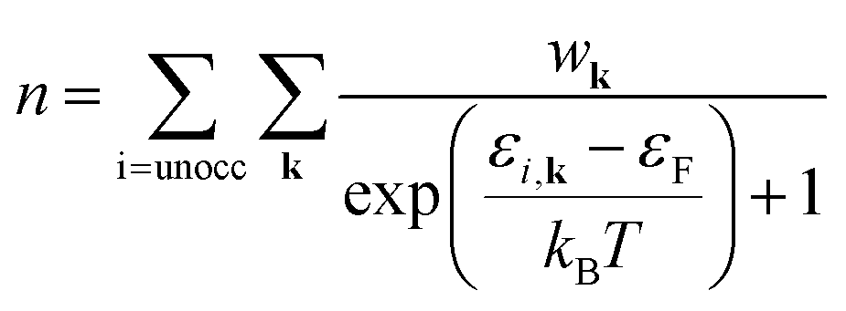
In thermodynamic equilibrium, the concentration (CDx) of a defect Dx is determined by Boltzmann statistics. Hence, if the Fermi level (ΔεF), the temperature (T), and the formation energy of the defect are known, eqn (3) can be used to obtain the concentration of an individual defect.
 | (3) |
 | (4) |
 | (5a) |
 | (5b) |
One-electron energies were estimated using 10 × 10 × 10 Γ-centered and Monkhorst–Pack k-point meshes in the conventional (8 atom) unit cell of γ-CuI. Tests performed using a PBE level of theory verified that a larger 30 × 30 × 30 k-mesh changed the calculated self-consistent Fermi level by ![[scr O, script letter O]](https://www.rsc.org/images/entities/char_e52e.gif) (−4) eV. The same order of magnitude changes were observed when comparing the results between the Monkhorst–Pack and Γ-centered meshes obtained with the PBE0 functional. The final values reported use an average of the two meshes in the self-consistent Fermi level calculation.
(−4) eV. The same order of magnitude changes were observed when comparing the results between the Monkhorst–Pack and Γ-centered meshes obtained with the PBE0 functional. The final values reported use an average of the two meshes in the self-consistent Fermi level calculation.
For charge neutrality in undoped CuI, six native defects were considered: VCu, VI, Cuint, CuI, Iint, and ICu. For both self-interstitials the Cu-tetrahedrally coordinated site was found to be energetically favorable. The formation energies of these defects as a function of the Fermi level are depicted in Fig. 7. We can see that the intrinsic vacancies and the Cu interstitial have the lowest formation energies and, thus, result in the highest defect concentrations in thermal equilibrium (see Fig. 8). Concentrations of the native substitutionals and the Iint were below 107 cm−3 in the entire temperature range considered under both Cu-rich and I-rich conditions and are, consequently, not visible in the plot. For most native defects our formation energy results show excellent agreement with a recent PBE0 study of Koyasu et al.,29 which investigated the link between optical properties and native defects in CuI. There are, however, two notable exceptions: (i) for the Iint defect we report a much lower (∼1.2 ev) formation energy likely due to a more favorable ionic relaxation and (ii) for the VI defect we report a deep thermodynamic transition to a q = −1 state discussed in more detail in the section n-type dopants.
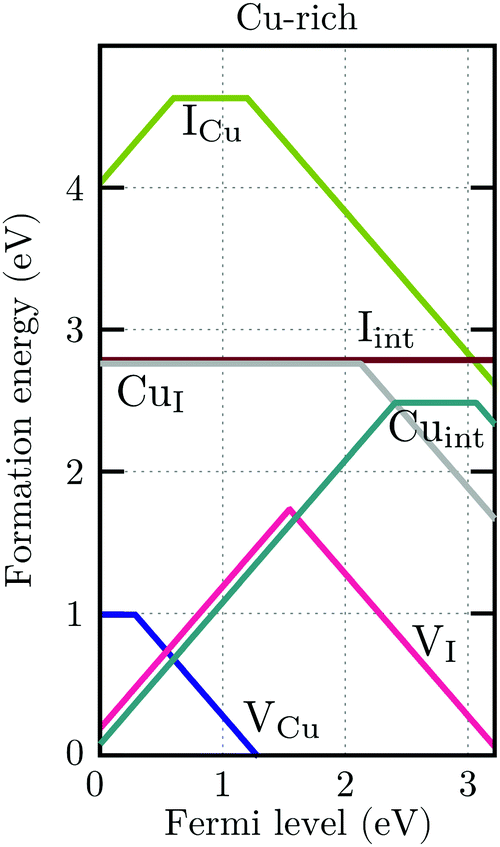 | ||
| Fig. 7 Formation energies of native defects in γ-CuI under Cu-rich conditions as a function of the Fermi level. Spontaneous formation of copper vacancies is anticipated at Fermi levels above 1.2 eV. | ||
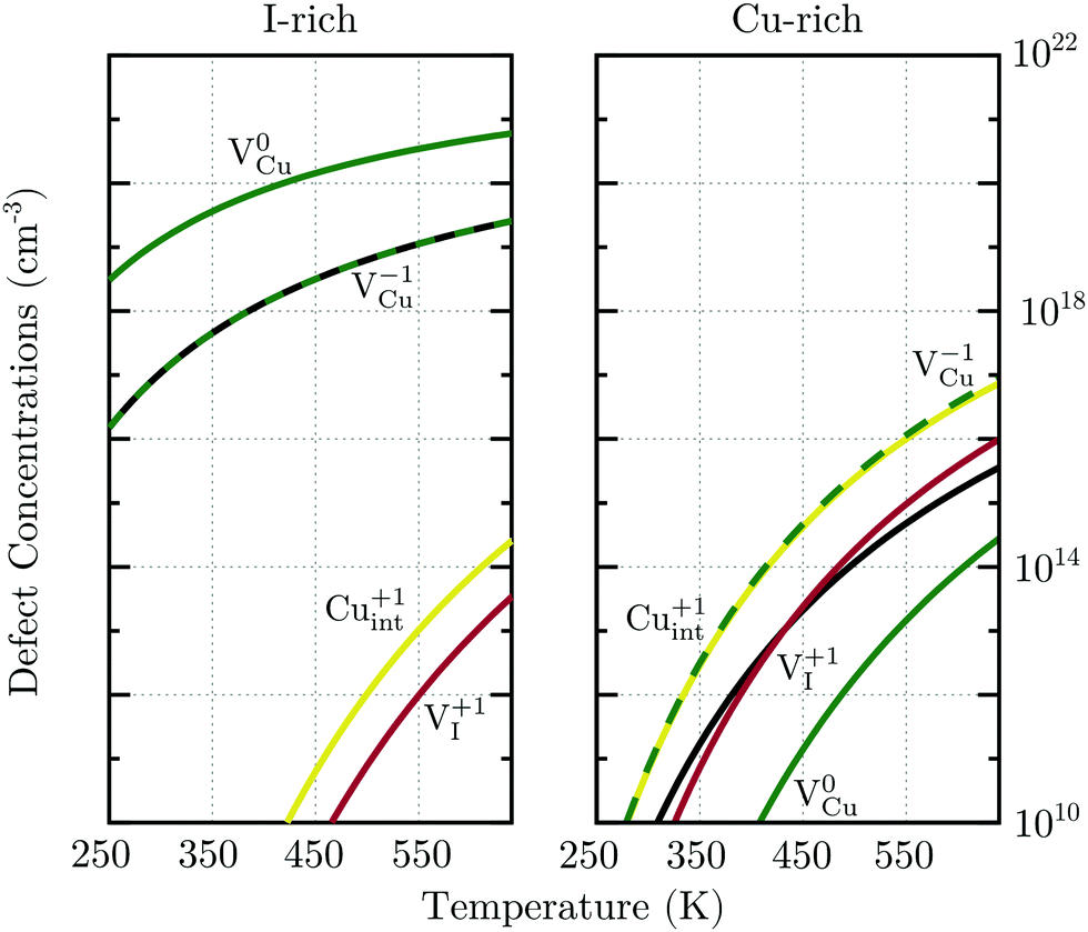 | ||
| Fig. 8 Thermal equilibrium native defect concentrations in undoped γ-CuI under I-rich and Cu-rich conditions. The corresponding number of holes delocalized in the valence band is indicated by solid black lines. | ||
Under I-rich conditions (left panel of Fig. 8) copper vacancies are seen to dominate. The most ubiquitous defect is the neutral copper vacancy (green-solid-line), with charged copper vacancies (green-dashed-line) present in concentrations two orders of magnitude lower. The Fermi level is pinned at 0.17 eV at room temperature and free-hole concentrations (solid-black-line) on the order of 1016 cm−3 are anticipated. This is in agreement with room temperature acceptor concentrations of p = 4.3 × 1016 cm−3 reported experimentally for bulk CuI.26 We predict that hole concentrations up to 1019 cm−3 are achievable by increasing the annealing temperature to just below the transition into β-CuI.
Under I-poor conditions (right panel of Fig. 8) copper vacancies (q = −1) and the compensating copper interstitials (q = +1) are present in similar concentrations. We note that Cuint (solid-yellow-line) and not VI (solid-red-line) are the dominant n-type defect in γ-CuI. The Fermi level is pinned at 0.55 eV at room temperature, resulting in acceptor carrier concentrations below 1010 cm−3. Under both Cu-rich and I-rich conditions electron concentrations are negligible in undoped γ-CuI.
Acknowledgements
M. G. acknowledges funding from the Swiss National Science Foundation under the Disco Project (No. CRSII2_154474). M. G. and J. A. F.-L. acknowledge computational resources under the projects (s707 and s752) from the Swiss National Supercomputing Center (CSCS) in Lugano. This work was supported by the NCCR-MARVEL funded by the Swiss National Science Foundation.References
- D. S. Ginley and J. D. Perkins, Handbook of transparent conductors, Springer, 2011, pp. 1–25 Search PubMed.
- E. Rucavado, M. Graužinytė, J. A. Flores-Livas, Q. Jeangros, F. Landucci, Y. Lee, T. Koida, S. Goedecker, A. Hessler-Wyser, C. Ballif and M. Morales-Masis, J. Phys. Chem. C, 2018, 122, 17612–17620 CrossRef CAS PubMed.
- S. C. Dixon, D. O. Scanlon, C. J. Carmalt and I. P. Parkin, J. Mater. Chem. C, 2016, 4, 6946–6961 RSC.
- A. Banerjee and K. Chattopadhyay, Prog. Cryst. Growth Charact., 2005, 50, 52–105 CrossRef CAS.
- H. Sato, T. Minami, S. Takata and T. Yamada, Thin Solid Films, 1993, 236, 27–31 CrossRef CAS.
- A. Zunger, Appl. Phys. Lett., 2003, 83, 57–59 CrossRef CAS.
- S. Lany and A. Zunger, Phys. Rev. Lett., 2007, 98, 045501 CrossRef.
- S. Nandy, A. Banerjee, E. Fortunato and R. Martins, Rev. Adv. Sci. Eng., 2013, 2, 273–304 CrossRef.
- H. Kawazoe, M. Yasukawa, H. Hyodo, M. Kurita, H. Yanagi and H. Hosono, Nature, 1997, 389, 939 CrossRef CAS.
- R. Nagarajan, N. Duan, M. Jayaraj, J. Li, K. Vanaja, A. Yokochi, A. Draeseke, J. Tate and A. Sleight, Int. J. Inorg. Mater., 2001, 3, 265–270 CrossRef CAS.
- A. Kudo, H. Yanagi, H. Hosono and H. Kawazoe, MRS Online Proc. Libr., 1998, 526, 299–303 CrossRef CAS.
- K. Ueda, S. Inoue, S. Hirose, H. Kawazoe and H. Hosono, Appl. Phys. Lett., 2000, 77, 2701–2703 CrossRef CAS.
- R. Nagarajan, N. Duan, M. Jayaraj, J. Li, K. Vanaja, A. Yokochi, A. Draeseke, J. Tate and A. Sleight, Int. J. Inorg. Mater., 2001, 3, 265–270 CrossRef CAS.
- J. Vidal, F. Trani, F. Bruneval, M. A. Marques and S. Botti, Phys. Rev. Lett., 2010, 104, 136401 CrossRef PubMed.
- F. Trani, J. Vidal, S. Botti and M. A. Marques, Phys. Rev. B: Condens. Matter Mater. Phys., 2010, 82, 085115 CrossRef.
- T. F. Cerqueira, S. Lin, M. Amsler, S. Goedecker, S. Botti and M. A. Marques, Chem. Mater., 2015, 27, 4562–4573 CrossRef CAS.
- J. Shi, T. F. Cerqueira, W. Cui, F. Nogueira, S. Botti and M. A. Marques, Sci. Rep., 2017, 7, 43179 CrossRef PubMed.
- R. Nagarajan, A. D. Draeseke, A. W. Sleight and J. Tate, J. Appl. Phys., 2001, 89, 8022–8025 CrossRef CAS.
- M. Grundmann, F.-L. Schein, M. Lorenz, T. Böntgen, J. Lenzner and H. von Wenckstern, Phys. Status Solidi A, 2013, 210, 1671–1703 CrossRef CAS.
- C. Yang, M. Kneiß, M. Lorenz and M. Grundmann, Proc. Natl. Acad. Sci. U. S. A., 2016, 113, 12929–12933 CrossRef CAS PubMed.
- N. Yamada, R. Ino and Y. Ninomiya, Chem. Mater., 2016, 28, 4971–4981 CrossRef CAS.
- B. Hönerlage, C. Klingshirn and J. Grun, Phys. Status Solidi B, 1976, 78, 599–608 CrossRef.
- D. Huang, Y.-J. Zhao, S. Li, C.-S. Li, J.-J. Nie, X.-H. Cai and C.-M. Yao, J. Phys. D: Appl. Phys., 2012, 45, 145102 CrossRef.
- O. Gogolin, J. Deiss and E. Tsitsichvili, Il Nuovo Cimento D, 1989, 11, 1525–1534 CrossRef.
- T. Chaudhuri, P. Basu, A. Patra, R. Saraswat and H. Acharya, Jpn. J. Appl. Phys., 1990, 29, L352 CrossRef CAS.
- D. Chen, Y. Wang, Z. Lin, J. Huang, X. Chen, D. Pan and F. Huang, Cryst. Growth Des., 2010, 10, 2057–2060 CrossRef CAS.
- S. Ves, D. Glötzel, M. Cardona and H. Overhof, Phys. Rev. B: Condens. Matter Mater. Phys., 1981, 24, 3073 CrossRef CAS.
- A. Gruzintsev and W. Zagorodnev, Semiconductors, 2012, 46, 35–40 CrossRef CAS.
- S. Koyasu, N. Umezawa, A. Yamaguchi and M. Miyauchi, J. Appl. Phys., 2019, 125, 115101 CrossRef.
- C. Yang, M. Kneiß, F.-L. Schein, M. Lorenz and M. Grundmann, Sci. Rep., 2016, 6, 21937 CrossRef CAS PubMed.
- S. Miyake, S. Hoshino and T. Takenaka, J. Phys. Soc. Jpn., 1952, 7, 19–24 CrossRef CAS.
- H. Hernández-Cocoletzi, G. H. Cocoletzi, J. Rivas-Silva, A. Flores and N. Takeuchi, J. Nano Res., 2009, 25–30 Search PubMed.
- J. P. Perdew, K. Burke and M. Ernzerhof, Phys. Rev. Lett., 1996, 77, 3865 CrossRef CAS PubMed.
- C. Adamo and V. Barone, J. Chem. Phys., 1999, 110, 6158–6170 CrossRef CAS.
- J. Paier, M. Marsman, K. Hummer, G. Kresse, I. C. Gerber and J. G. Ángyán, J. Chem. Phys., 2006, 124, 154709 CrossRef CAS PubMed.
- J. Heyd, G. E. Scuseria and M. Ernzerhof, J. Chem. Phys., 2003, 118, 8207–8215 CrossRef CAS.
- J. Heyd, G. E. Scuseria and M. Ernzerhof, J. Chem. Phys., 2006, 124, 219906 CrossRef.
- S. Hull and D. Keen, Phys. Rev. B: Condens. Matter Mater. Phys., 1994, 50, 5868 CrossRef CAS PubMed.
- E. Wiberg, Die chemische Affinität, Verlag de Gruyter, 2nd edn, 1972 Search PubMed.
- D. R. Lide, CRC handbook of chemistry and physics, internet version 2005, 2005 Search PubMed.
- F. Tran and P. Blaha, J. Phys. Chem. A, 2017, 121, 3318–3325 CrossRef CAS PubMed.
- M. Cardona, Phys. Rev., 1963, 129, 69 CrossRef.
- A. Blacha, M. Cardona, N. Christensen, S. Ves and H. Overhof, Solid State Commun., 1982, 43, 183–187 CrossRef CAS.
- A. Alkauskas, M. D. McCluskey and C. G. Van de Walle, J. Appl. Phys., 2016, 119, 181101 CrossRef.
- C. Freysoldt, B. Grabowski, T. Hickel, J. Neugebauer, G. Kresse, A. Janotti and C. G. Van de Walle, Rev. Mod. Phys., 2014, 86, 253 CrossRef.
- M. Graužinytė, S. Goedecker and J. A. Flores-Livas, Chem. Mater., 2017, 29, 10095–10103 CrossRef.
- M. Graužinytė, S. Goedecker and J. A. Flores-Livas, Phys. Rev. Mater., 2018, 2, 104604 CrossRef.
- J. Wang, J. Li and S.-S. Li, J. Appl. Phys., 2011, 110, 054907 CrossRef.
- H. Chen, C.-Y. Wang, J.-T. Wang, Y. Wu and S.-X. Zhou, Phys. B, 2013, 413, 116–119 CrossRef CAS.
- M. Xia, M. Gu, X. Liu, B. Liu, S. Huang and C. Ni, J. Mater. Sci.: Mater. Electron., 2015, 26, 5092–5096 CrossRef CAS.
- G. Kresse and J. Furthmüller, Phys. Rev. B: Condens. Matter Mater. Phys., 1996, 54, 11169 CrossRef CAS PubMed.
- G. Kresse and J. Furthmüller, Comput. Mater. Sci., 1996, 6, 15–50 CrossRef CAS.
- P. E. Blöchl, Phys. Rev. B: Condens. Matter Mater. Phys., 1994, 50, 17953 CrossRef PubMed.
- G. Kresse and D. Joubert, Phys. Rev. B: Condens. Matter Mater. Phys., 1999, 59, 1758 CrossRef CAS.
- Y. Kumagai and F. Oba, Phys. Rev. B: Condens. Matter Mater. Phys., 2014, 89, 195205 CrossRef.
- D. Broberg, B. Medasani, N. E. Zimmermann, G. Yu, A. Canning, M. Haranczyk, M. Asta and G. Hautier, Comput. Phys. Commun., 2018, 226, 165–179 CrossRef CAS.
- J. Potts, R. Hanson, C. Walker and C. Schwab, Solid State Commun., 1973, 13, 389–392 CrossRef CAS.
Footnotes |
| † Electronic supplementary information (ESI) available: Reference phase data, PBE0 atomic relaxation tests, and defect concentrations (I-rich conditions). See DOI: 10.1039/c9cp02711d |
| ‡ European theoretical spectroscopy facility. |
| This journal is © the Owner Societies 2019 |