
 Open Access Article
 This Open Access Article is licensed under a
 Creative Commons Attribution 3.0 Unported Licence
Femtosecond laser generation of microbumps and nanojets on single and bilayer Cu/Ag thin films†
Aida
Naghilou‡
 *a,
Miao
He‡
b,
Jasmin S.
Schubert
a,
Leonid V.
Zhigilei
ab and
Wolfgang
Kautek
a
*a,
Miao
He‡
b,
Jasmin S.
Schubert
a,
Leonid V.
Zhigilei
ab and
Wolfgang
Kautek
a
aUniversity of Vienna, Department of Physical Chemistry, Vienna, Austria. E-mail: aida.naghilou@univie.ac.at
bUniversity of Virginia, Department of Materials Science and Engineering, Charlottesville, Virginia, USA
First published on 15th May 2019
Abstract
The formation mechanisms of microbumps and nanojets on films composed of single and double Cu/Ag layers deposited on a glass substrate and irradiated by a single 60 fs laser pulse are investigated experimentally and in atomistic simulations. The composition of the laser-modified bilayers is probed with the energy dispersive X-ray spectroscopy and used as a marker for processes responsible for the modification of the film morphology. For the bilayer with the top Ag layer facing the laser, the increase in fluence is found to result in a sequential appearance of a Ag microbump, the exposure of the Cu underlayer by removal of the Ag layer, a Cu microbump, and a frozen nanojet. The Cu on Ag bilayer exhibits a partial spallation of the top Cu film, followed by the generation of surface structures that mainly consist of Ag at higher fluences. The experimental observations are explained with atomistic simulations, which reveal that the stronger electron–phonon coupling of Cu results in the confinement of the deposited laser energy in the top Cu layer in the Cu on Ag case and channelling of the energy from the top Ag layer to the underlying Cu layer in the Ag on Cu case. This difference in the energy (re)distribution directly translates into differences in the morphology of the laser-modified bilayers. In all systems, the generation of microbumps and nanojets occurs in the molten state. It is driven by the dynamic relaxation of the laser-induced stresses and, at higher fluences, the release of vapor at the interface with the substrate. The resistance of the colder periphery of the laser spot to the ejection of spalled layers as well as the rapid solidification of the transient molten structures are largely defining the final shapes of the surface structures.
1. Introduction
Ultrafast lasers are a peerless tool for high-precision processing of various materials,1,2 including dielectrics,3–10 semiconductors,11–14 and metals.1,15–19 It has been demonstrated that laser irradiation can modify material microstructure and create a wide variety of surface morphologies. These can vary from random micro- and nanostructures,20–22 subsurface voids and microcracks,23–25 to laser-induced periodic surface structures or “ripples”,13,18,26–30 which are to a certain extent controlled by the laser wavelength and polarization, to micro/nanobumps and frozen nanojets generated with single tightly-focused ultrashort pulses.31–43 The latter surface structures can be replicated into ordered arrays by means of interference between multiple beams.31,44 The surfaces with arrays of metallic and non-metallic microbumps have many potential technological applications due to their unique properties, such as superhydrophobicity,45,46 self-cleaning,47 and enhanced tribological performance,48 as well as their active and nonlinear optical response.49While the generation of microbumps and nanojets has been reproduced in many studies, the mechanisms behind their formation are still being debated. It is generally accepted39,50 that frozen nanojets are produced through rapid melting, jetting of the molten material driven by pressure gradients, and rapid cooling of the melt leading to the freezing of the nanojets. The processes responsible for the formation of microbumps, however, are still under discussion. In particular, the Marangoni effect,40 subsurface boiling and pressure of the vapor released at the substrate-film interface,31,36 melting and redistribution of molten material,39–42,51,52 and plastic deformation of the irradiated film35,53 have been suggested as processes responsible for the formation and rupturing of the microbumps.
Large-scale atomistic modelling of thin nickel films irradiated by a single femtosecond pulse51,52 supports the scenario of the microbump formation in the course of the transient melting and resolidification. The simulations show that rapid localized laser heating and melting of the film takes place under partial inertial stress confinement,54 leading to a buildup of compressive stresses. The relaxation of these compressive stresses is identified as the main driving force causing the upward acceleration of the melted region of the film, its delamination from the substrate, and eventual formation of a bump. The shape of the bump is defined by the competition of the hydrodynamic flow of the molten part of the film and the solidification occurring under conditions of strong undercooling caused by fast two-dimensional electron heat transfer from the laser heated region. The simulations predict that the undercooling can reach the levels required for the onset of massive homogeneous nucleation of new crystallites, leading to the formation of nanocrystalline structure of the frozen bump. Theoretical and experimental studies on gold thin films support the role of melting in the formation of microbumps as well.39–42
On the other hand, the possibility of the formation of microbumps without melting was suggested based on continuum-level elasto-plastic flow modelling combined with the two-temperature model calculations performed for gold films irradiated by a femtosecond pulse.53 In the process of deformation, the film gains momentum normal to the surface and undergoes plastic deformations that dissipate the energy of the outward motion into the work of plastic deformations. While the film is assumed to remain solid in the course of the bump formation, thermal softening of the laser-heated region can reduce the yield strength of the metal and facilitate the plastic deformation.
We note that the alternative mechanisms of the microbump formation discussed above are not mutually exclusive and the relative contribution of these mechanisms can be defined by the material properties, irradiation conditions, film thickness and adhesion to the substrate. In particular, material properties such as low adhesion to the substrate, negative material density change upon melting contributing to the buildup of the initial compressive stresses, as well as sufficiently high values of surface tension and viscosity capable of suppressing the breakup of the transient molten structures are essential for the bump generation through melting and resolidification.39 For the microbump formation in the solid state through plastic deformation, on the other hand, high values of the Young's modulus and coefficient of thermal expansion are required for effective generation of the initial stresses, and a high ductility is needed to support large plastic deformation.53 The scenario of vapor pressure driving the film deformation and microbump formation31,36 requires high values of vapor pressure at temperatures where the molten film still retains its integrity.
Most of the experimental studies of the laser-induced generation of microbumps and nanojets have been performed on gold films31–35,39–42,44 and, depending on the assumed model, the successful generation of high-quality surface structures has been attributed to either mechanical properties of solid Au53 or thermophysical properties of the molten Au.39 However, with a suitable choice of irradiation conditions, the single pulse generation of nanojets and/or microbumps has also been observed for other materials, including silver36,37,39 and copper39 films, silicon film irradiate by a nanosecond pulse,55 and bulk glass targets covered by a polymer or water overlayers.56,57
In this study, we investigate the mechanisms responsible for the formation of microbumps and nanojets on films composed of double and single layers of Cu and Ag deposited on a glass substrate and irradiated by a single femtosecond laser pulse. The advantage of the multi-layered targets has been demonstrated in recent studies of the mechanisms of laser-induced ripple formation in a multi-pulse irradiation regime,58 as well as nanostructuring by a single femtosecond X-ray vortex pulse.59 Analysis of the elemental composition of the laser-processed surfaces and target cross-sections provides valuable information on the extent of melting and heat affected zones. In the present work, our choice of the Ag–Cu system, a eutectic binary alloy with very limited solubility in the solid state,60 ensures that any significant mixing of the two components can only occur in the liquid state. Therefore, the observation of the elemental mixing in the double layer bumps would be an unequivocal indication of melting. An additional factor in choosing the Ag–Cu system is the large difference in the strength of the electron–phonon coupling factor between the two metals, allowing the exploration of the implications of the energy redistribution in the electronically excited state for the final morphology of the laser-generated surface structures.
2. Methods
2.1 Laser irradiation experiments
The experiments were performed for Ag, Cu, and Ag–Cu bilayer films prepared by thermal evaporation (EPA101, Anton Paar) on microscope glass slides. The layer thickness was controlled with an online quartz crystal microbalance deposition monitor. The single component systems were Ag and Cu films with a thickness of 50 ± 5 nm. The bilayers samples were twice thicker and consisted of two 50 ± 5 nm thick layers, either Ag on Cu or Cu on Ag.The samples were irradiated by a Ti:Sapphire Chirped Pulse Oscillator (modified Femtosource XL, Femtolasers Produktions GmbH) delivering pulses with a full width at half maximum duration of 60 fs at a central wavelength of 800 nm with a repetition rate of 11 MHz. Pulses were selected with a Pockels cell based pulse picker. The focus position was determined by a custom in situ system.61 All experiments were performed under vacuum (10−2 mbar) and with a beam radius of w = 1.40 ± 0.06 μm.
After the laser irradiation, all samples were characterized by optical microscopy (OM; STM-MJS, Olympus) and scanning electron microscopy (SEM; Supra 55VP, Zeiss) with integrated energy dispersive X-ray spectroscopy (EDX).
2.2 Computational model
To obtain insights into the mechanisms responsible for the modification of surface morphologies, a series of atomistic simulations were performed with a hybrid model combining the classical molecular dynamics (MD) method representation of the laser-induced structural and phase transformations with a continuum-level description of laser excitation of conduction band electrons and following electron–phonon equilibration based on two-temperature model (TTM). A detailed description of the TTM-MD model can be found in ref. 62–64, and below we only provide parameters of the computational setup specific for the simulations reported in this paper.The interatomic interactions in the MD part of the TTM-MD model are described by the embedded atom method (EAM) potential in the form suggested by Foiles, Baskes, and Daw (FBD).65 The potential functions are fitted to the sublimation energies, equilibrium lattice constants, elastic constants, and vacancy formation energies for pure metals and fitted to the heat of mixing for cross-interactions in dilute binary solid solutions. A cutoff function66 is added to the potential, which brings the interaction energies and forces to zero at a cutoff distance of 5.5 Å. The melting temperatures of FBD EAM Ag and Cu, 1139 ± 2 K and 1288 ± 2 K, respectively, are evaluated in ref. 67 and are found to agree reasonably well with experimental values. The critical temperatures estimated based on the test area method68 calculation of the temperature dependence of the surface tension are 3380 ± 11 K and 5767 ± 39 K for the FBD EAM Ag and Cu, respectively.
The complete description of the dynamic response of an irradiated film to the laser energy deposition leading to the formation of a microbump is beyond the capabilities of atomistic MD method. Thus, the simulations reported in this paper are not aimed at directly reproducing the formation of a microbump but focus on the analysis of the thermodynamic driving forces responsible for the laser-induced material removal and redistribution. The processes occurring in the central part of the laser spot are investigated with computational systems representing the bilayer films deposited on a silica glass substrate. The vertical dimensions of computational systems are chosen to match those of metal bilayers deposited on silica glass studied in the experiments. The bilayer films are prepared by combining two 50 nm-thick Ag and Cu films with fcc crystal structure and (001) orientation of the interface. Periodic boundary conditions are applied in the lateral directions, and the lateral size of the computational system is 6.54 nm × 6.54 nm, which corresponds to 18 unit cells for the Cu film and 16 slightly compressed unit cells for the Ag film.
The glass–metal interaction and the elastic response of the silica glass are also reproduced in the model. The silica glass substrate is described by an imaginary plane that interacts with the bottom metal layer through the method described in ref. 69. Briefly, the interactions between the atoms of the bottom layer and the substrate are represented by the Lennard-Jones (LJ) potential, parameterized to reproduce the experimental value of adhesion energy,70 as well as the local stiffness of the interface under uniaxial compression, which is defined by an arithmetic average of the elastic constants C11 for EAM-FBD metal65 and fused silica.71 The corresponding parameters of the LJ potential are σ = 2.951 Å and ε = 0.223 eV for Ag–SiO2 interaction and σ = 4.693 Å and ε = 0.267 eV for Cu–SiO2 interaction, where σ is the distance at which the interaction potential is zero, and ε is the depth of the potential well. The displacement of the imaginary plane is controlled by dynamic acoustic impedance matching boundary condition69 that provides a computationally efficient description of the partial reflection of the laser-induced pressure wave from the metal–silica interface. The combined systems of bilayer films deposited on the silica substrate are equilibrated at 300 K before laser irradiation.
The description of the electron and lattice temperature dependences of the electron–phonon coupling factor and electron heat conductivity of Ag and Cu included in the TTM equations account for the thermal excitation from the electron states below the Fermi level.72 The temperature dependence of the electron thermal conductivity is described by the Drude model relation fitted to the experimental values of thermal conductivity of solid Cu and Ag at the melting temperature.67 The thermal boundary resistance for the electronic energy transfer through the Ag–Cu interface is not included in the model. While the values of thermal boundary resistance revealed in time-resolved thermoreflectance experiments73–75 are sufficiently high to have practical implications on the electronic heat transfer in nanoscale metal multilayers, all of these measurements were done at laser fluences that induce very small, in the range of tens of Kelvin, temperature changes in the irradiated material. The results of thermoreflectance measurements are found to follow the predictions of the electron diffuse mismatch model, which predicts a linear increase of the interface conductance with electron temperature. Under irradiation conditions used in the experiments reported in this paper, the electron temperature reaches the maximum values in the range of ten thousand Kelvin, which is expected to completely erase the effect of the finite interface conductance and produce thermalization of electrons on a timescale of less than 1 ps. This conclusion is consistent with the results of a recent study of the heat transfer in Au–Ni bilayer system with ultrafast X-ray diffraction, reported in ref. 76. The stronger pump pulse used in this experiment produces an electron temperature increase on the order of thousands of Kelvin, and the results of ultrafast diffraction probing are found to be incompatible with any significant electronic interface resistance between the two metal layers.
A source term is added to the TTM equation for the electron temperature, describing the energy deposition by a 60 fs laser pulse with a Gaussian temporal profile. An exponential attenuation of laser intensity with the depth under the target surface is assumed, and the effective range of laser energy deposition is approximated as a sum of the optical absorption depth and the ballistic electron penetration depth.77,78 The estimation of the ballistic electron penetration depth is provided in ref. 79, giving the effective penetration depth of 28 nm for Cu and 65 nm for Ag. The simulations are performed at absorbed fluences ranging from 0.03 J cm−2, which is slightly below the melting threshold, to 0.4 J cm−2, where both layers are removed from the substrate. To facilitate comparison of the computational results with experimental observations, the incident laser fluence is estimated for each of the absorbed laser fluences by performing TTM calculations accounting for the electron temperature dependence of the reflectivity and optical absorption coefficient, as described in the ESI.†
3. Results and discussion
In this work we perform a systematic evaluation of the mechanisms of generation of microbumps and nanojets on metal films deposited on a silica glass substrate and irradiated by a single 60 fs laser pulse. First, the results obtained for 50 nm-thick one-component Ag and Cu films are briefly discussed and related to the earlier reports. A more complex picture of the laser-induced modification and damage of bilayer films consisting of two 50 nm-thick layers, either Ag on Cu or Cu on Ag is then presented, and the interpretation of the experimental observations is assisted by analysis of the results of atomistic modelling.For all films, the range of laser fluences was chosen to cover all possible outcomes of the laser irradiation: starting from a fluence above complete film breaching threshold, the fluence was reduced by 2% of the previous value until a level below the threshold of visible modification of the film is reached. The modification threshold fluence was determined by OM as the fluence required for the onset of irreversible morphological alteration (change in reflectivity, localized ablation) without bump formation. The fluence resulting in an elevation/bulging of the film was defined as bump formation threshold fluence and was determined by SEM. The generation of jets above the jet formation threshold fluence was also observed by SEM. At the film breaching threshold fluence, the bumps start to break and rupture and reveal the underlying material in OM. All threshold fluences were determined based on the probability method.80–83 In Fig. 1, the threshold fluences for modification, bump formation, bump breaching, and jet formation for each sample are presented. The respective breached layer is denoted on the bump breaching data to indicate whether the breaching took place in a mixed or in a single layer. The incident fluence Finc data of Fig. 1a were converted to absorbed fluences Fabs in Fig. 1b using TTM calculations discussed in the ESI.†
 | ||
| Fig. 1 Threshold fluences Fth for modification, bump formation, bump breaching, and jet formation observed in single pulse laser irradiation of Ag and Cu films and Ag–Cu bilayers. The breached layer is denoted on the respective column. The results are shown for the incident fluence in (a) and absorbed fluence in (b), with conversion explained in ESI.† | ||
3.1 Single layers
The values of the threshold fluences shown for the single layers of Ag and Cu in Fig. 1 indicate that the bump formation and breaching thresholds are very close to each other. Actually, for Ag films only cracked and breached microbumps are observed, with two representative SEM images shown in Fig. 2. For Cu films, the bumps were breached at fluences about 10% above the bump formation threshold, with typical melting features observed in the SEM images, Fig. 3. The two bumps shown in Fig. 3 are generated at a fluence identified as the bump breaching threshold, and a statistical coexistence of both breached and intact bumps is observed. Frozen nanojets are observed for neither Ag nor Cu films. Thus, we conclude that for the film thickness of 50 nm and the focusing conditions used in the experiments, a reproducible deterministic generation of intact microbumps is not possible for Ag and can only be realized in a very narrow range of fluences for Cu.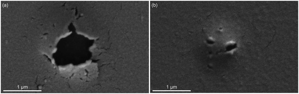 | ||
| Fig. 2 Single Ag layer (50 nm, on glass). Scanning electron micrographs of microbump breaching. Finc = 2.11 J cm−2, Fabs = 0.25 J cm−2, N = 1, w = 1.40 ± 0.06 μm. | ||
 | ||
| Fig. 3 Single Cu layer (50 nm, on glass). Scanning electron micrographs of the (a) microbump formation and (b) breaching. Finc = 0.40 J cm−2, Fabs = 0.02 J cm−2, N = 1, w = 1.40 ± 0.06 μm. Microbump formation and breaching occur statistically at this parameter set. | ||
These observations are consistent with earlier reports. In contrast to Au films commonly used for the generation of microbumps/nanojets by single pulse laser irradiation,31–35,39–42,44 it was found in ref. 39 that no stable nanojet structures can be obtained for a 60 nm-thick Ag film, which was attributed to a lower surface tension of Ag as compared to Au. The formation of a frozen jet has been demonstrated for a 60 nm-thick Cu film, albeit only for conditions of tight focusing of the laser beam on the back side of the film.39 In a systematic study of the fluence dependence of the surface structures generated on Ag films with thicknesses ranging from 50 to 380 nm,37 it was found that only breached bumps can be formed on 50 nm-thick films, while intact bumps and frozen nanojets can be produced on thicker films.
In addition to the difference in surface morphology, Fig. 1 also reveals that the threshold fluences for modification and bump breaching are much lower in Cu film than in Ag film. As will be discussed later, Cu has much stronger electron–phonon coupling and much shorter electron mean free path as compared to Ag. Both of these factors contribute to a much stronger confinement of the deposited laser energy in the surface region of Cu film, which partially explains the substantially lower modification and damage thresholds observed for Cu.
3.2 Double layers
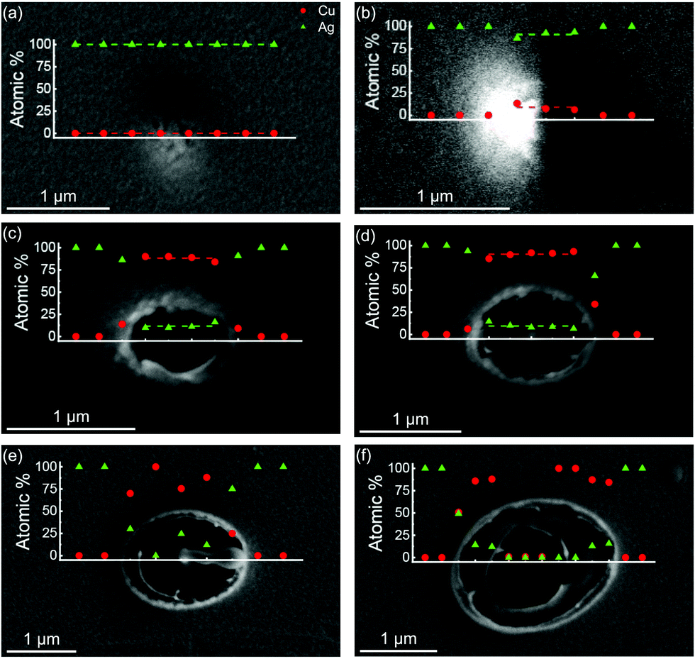 | ||
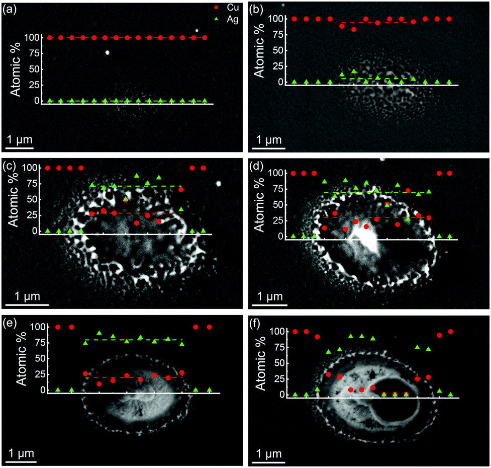
| Fig. 4 Ag on Cu (50 nm each, on glass). Scanning electron micrographs of irradiated spots overlain with EDX line scans. (a) Finc = 1.73 J cm−2, Fabs = 0.16 J cm−2, (b) Finc = 1.92 J cm−2, Fabs = 0.20 J cm−2, (c) Finc = 2.00 J cm−2, Fabs = 0.22 J cm−2, (d) Finc = 2.18 J cm−2, Fabs = 0.27 J cm−2, (e) Finc = 2.70 J cm−2, Fabs = 0.45 J cm−2, (f) Finc = 3.16 J cm−2, Fabs = 0.66 J cm−2. N = 1, w = 1.40 ± 0.06 μm. The x-axes represent the EDX scan lines. Green triangles: silver, red dots: copper, dashed lines mark the average values. | ||
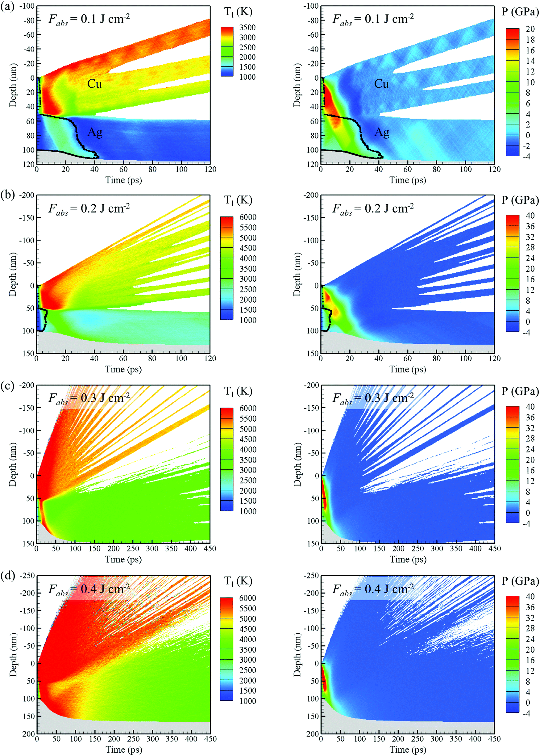
In order to assist with interpretation of the experimental observations, a series of atomistic simulations were performed for Ag on Cu double layer under irradiation conditions comparable to those used in the experiments. A hybrid model combining TTM with the classical MD method was used in all of the simulations (see Section 2.2 for the description of the TTM-MD model). The contour plots in Fig. 5 show the evolution of the lattice temperature and pressure in the target irradiated at the absorbed fluences of 0.1, 0.2, 0.3, and 0.4 J cm−2. Most of the laser energy is deposited within the top Ag layer, leading to a substantially higher electron temperature in the Ag layer generated by the end of the laser pulse. Nevertheless, the lattice temperature in the Cu layer increases faster than in the Ag layer and reaches much higher maximum values, as can be seen from the left panels of Fig. 5. This behavior can be explained by more than twice stronger electron–phonon coupling in Cu as compared to Ag at room temperature and even larger difference between the two materials in the electronically excited state due to the stronger contribution of thermally excited d-band electrons in Cu.67,72 The hot electrons in the Ag layer rapidly equilibrate with the electrons in the Cu layer, which in turn equilibrate with phonons, leading to the preferential heating of the Cu layer. A similar effect of sub-surface heating in femtosecond laser interactions with layered targets has been predicted in TTM calculations performed for Au–Cr targets86 and in TTM-MD simulations of Au–Cu78 and Ag–Cu67 targets. Experimentally, the electronic energy redistribution under conditions of electron–phonon nonequilibrium has been used to explain the results of time-resolved pump–probe thermoreflectivity measurements performed for Au–Cr87 and Au–Pt88 layered systems.
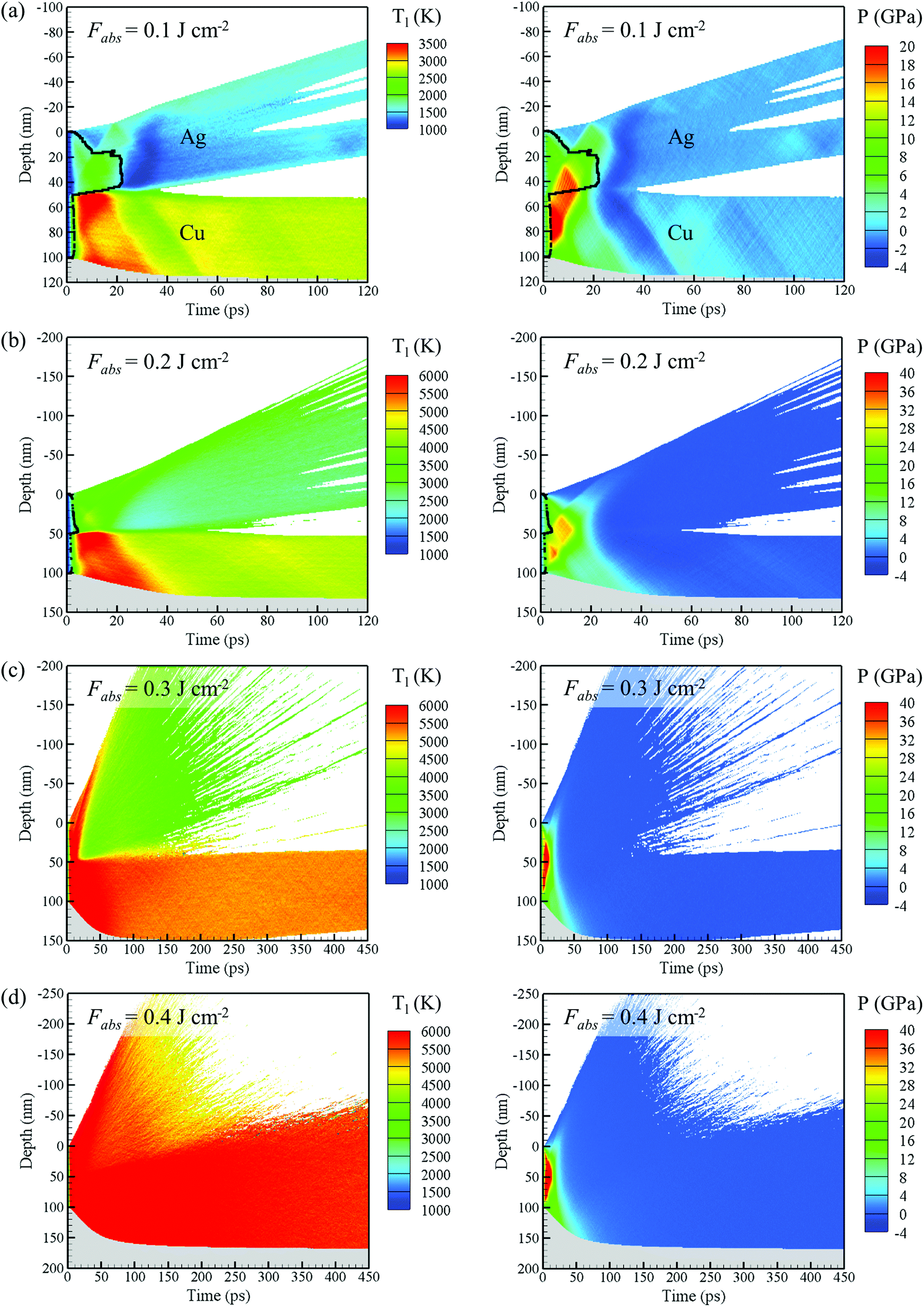 | ||
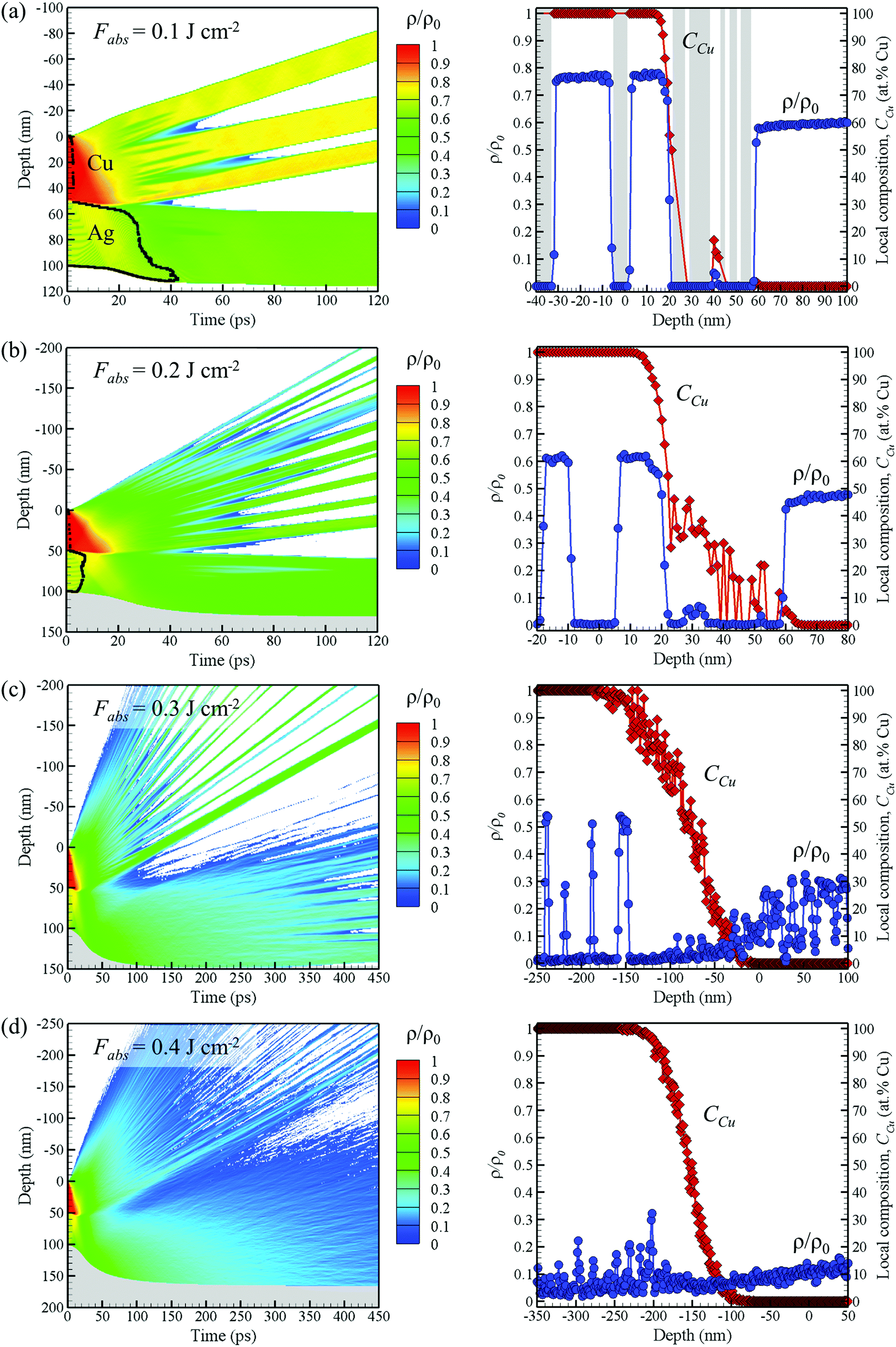
| Fig. 5 Spatial and temporal evolution of lattice temperature Tl and pressure P predicted in TTM-MD simulations of Ag on Cu bilayer system irradiated by a 60 fs laser pulse at (a) Fabs = 0.1 J cm−2, Finc = 1.4 J cm−2, (b) Fabs = 0.2 J cm−2, Finc = 1.9 J cm−2, (c) Fabs = 0.3 J cm−2, Finc = 2.3 J cm−2, and (d) Fabs = 0.4 J cm−2, Finc = 2.6 J cm−2. The black lines in (a) and (b) represent the solid–liquid interfaces which outline the solid parts of the film. The black lines are not shown in (c) and (d) where fast homogeneous melting is completed within ∼4 ps. The grey regions represent the silica substrate. Regions with relative atomic density ρ/ρ0 of less than 0.07 are blanked, where ρ0 is the density of Cu at 300 K. | ||
At the lowest absorbed fluence of 0.1 J cm−2, the preferential subsurface heating and melting of the Cu substrate is apparent from Fig. 5a, where the Cu layer can be seen to melt within several picoseconds following the laser excitation, while the lower part of the Ag layer remains solid up to about 20 ps. The rapid heating and melting of the top part of the Cu layer leads to the generation of compressive stresses that drive compressive waves propagating into the overlaying Ag layer and towards the glass substrate. The complete reflection of the compressive wave from the top surface of the film and partial reflection from the substrate (the acoustic impedance of silica glass is less than half of that of Cu) result in the generation of tensile waves. These waves converge on the interface between the layers and create tensile stresses sufficient for delamination of the film into Ag and Cu parts, with the Ag layer further separating into several parts at a later time. In contrast to the ejection of the Ag layer in the quasi-one-dimensional TTM-MD simulation performed with a relatively small lateral size of the computational cell, under experimental conditions of irradiation by a tightly focused laser beam, the delaminated Ag layer can be expected to decelerate due to its interaction with the surrounding colder material at the periphery of the laser spot, leading to the formation of a Ag bump similar to that observed in Fig. 4a and b. According to the TTM calculations discussed in the ESI,† the absorbed fluence of 0.1 J cm−2 is realized at about 1.4 J cm−2 of incident fluence, which is comparable to the fluence producing the bump shown in Fig. 4a.
At an absorbed fluence of 0.2 J cm−2 (∼1.9 J cm−2 incident fluence), the temperature of Ag film is brought near the critical temperature (estimated as 3380 K for FBD EAM Ag), leading to an explosive decomposition and removal of the Ag film, Fig. 5b. The temperature of the top part of the Cu layer also approaches the critical temperature (estimated as 5767 K for FBD EAM Cu) for a short time, but the decomposition of the Cu layer is suppressed by the pressure generated by the expanding plume produced by the explosive decomposition of the Ag layer. The ejection of the top Ag layer reveals the underlying Cu layer that can be expected to remain on the substrate. This scenario can be related to the experimentally observed breaching of Ag microbump, Fig. 4c, at a fluence similar to that used in the simulation.
At a higher absorbed fluence of 0.3 J cm−2 (∼2.3 J cm−2 incident fluence, Fig. 5c), the pressure from the Ag layer undergoing the phase explosion can no longer suppress the separation of the Cu layer from the substrate. The temperature of the Cu layer at the time of its separation from the substrate (appearance of a white low-density region near the substrate at ∼250 ps) remains close to the critical temperature, and the separation is driven by pressure from vapor released at the Cu-substrate interface. Nevertheless, the Cu layer retains its integrity during the simulation, suggesting that, similarly to the Ag layer in the simulation performed at Fabs = 0.1 J cm−2, the deceleration due to the interaction of the layer with the surrounding colder material, as well as the Ag vapor pressure from above, can prevent the ejection of the layer and lead to the formation of a Cu microbump and/or frozen nanojet similar to those shown in Fig. 4d and e.
Finally, at an absorbed fluence of 0.4 J cm−2 (∼2.6 J cm−2 incident fluence, Fig. 5d), both Ag and Cu layers undergo an explosive decomposition into vapor and liquid droplets, leading to the complete removal of the bilayer film from the substrate. While the decomposition of the Cu layer into the mixture of vapor and small liquid droplets is difficult to see from the temperature and pressure contour plots shown in Fig. 5, it is apparent in the corresponding density plot shown in Fig. 6d discussed below. The fluence required for the complete film removal predicted in the simulations is in a good quantitative agreement with the experimentally measured threshold fluence for Cu bump breaching, Finc ≈ 2.8 J cm−2 (Fig. 1) and the formation of a hole in the bilayer film (Fig. 4f).
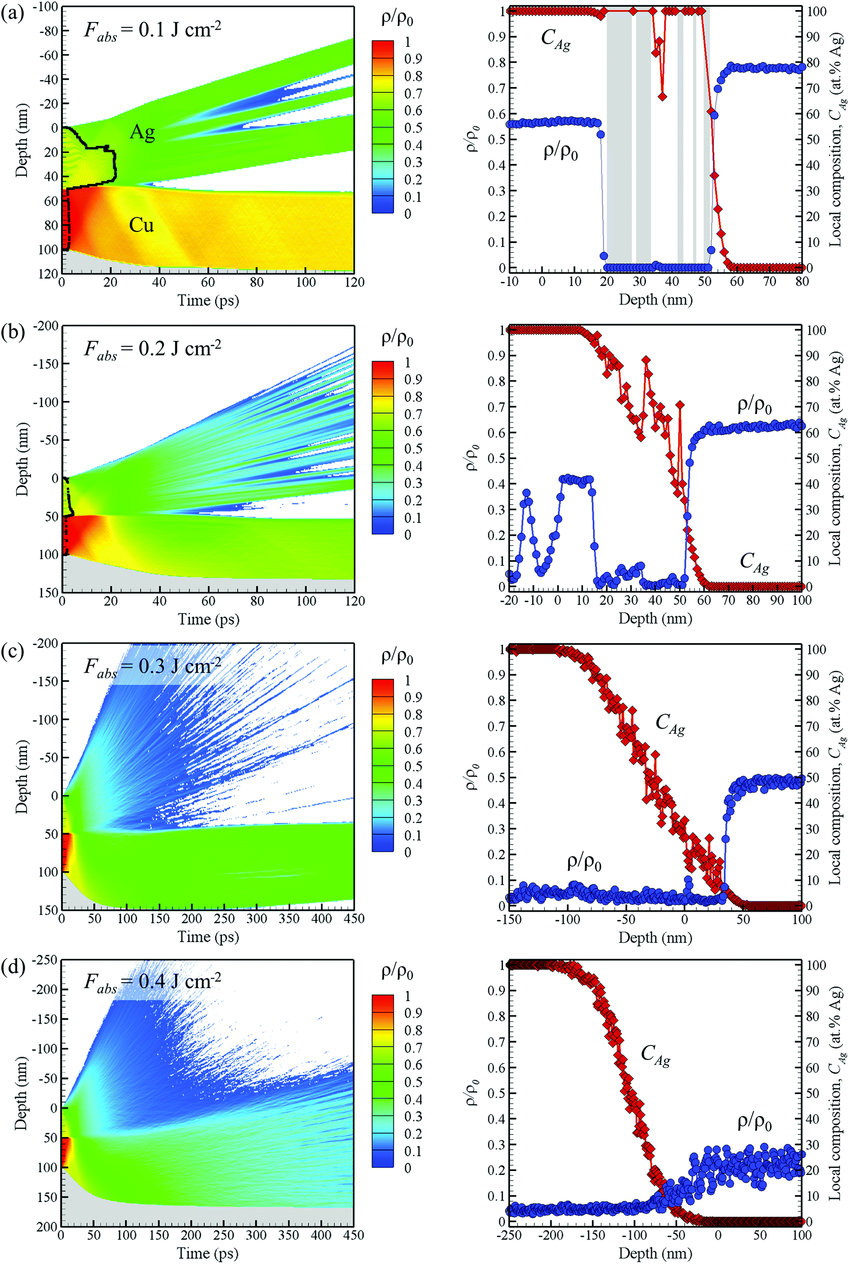 | ||
| Fig. 6 Spatial and temporal evolution of local density ρ normalized to the density of Cu at 300 K, ρ0 (left panels) and the distribution of normalized density and the elemental composition in the mixing regions at the end of simulations (right panels) shown for the simulations illustrated by Fig. 5. In the left panels, the regions where the normalized density is below 0.07 are blanked, the grey regions represent the silica substrate, and the black lines correspond to solid–liquid interfaces that outline the solid parts. In the right panel of (a), the grey areas show the regions of zero density, where the composition cannot be defined. | ||
In order to facilitate the connection between the computational predictions and the experimental EDX line scans, the density and composition profiles calculated for systems obtained by the end of the TTM-MD simulations are plotted, along with the density contour plots, in Fig. 6. The system is divided into layers with thickness of 1 nm along depth, and the normalized density ρ/ρ0 is calculated by dividing the local density in each layer by the density of solid Cu at 300 K. The regions where ρ/ρ0 is less than ∼0.1 can be regarded as regions where only vapor and small clusters of atoms are present. The density and composition profiles in the right panels of Fig. 6 are plotted in blue and red colours, respectively, and are calculated for the last moment of time shown in the contour plots in the left panels of Fig. 6.
Below the threshold for the Ag layer breaching/removal, where the ejection of the Ag film from the centre of the laser spot is expected to be suppressed by the interaction with surrounding colder regions, the EDX data mainly register Ag atoms but also detect a small fraction of Cu, Fig. 4b. As can be seen from the right panel of Fig. 6a, the mixing between the two layers is very limited at this fluence, and the Cu signal in Fig. 4b is likely to be related to thinning of the Ag layer at the centre of the laser spot during the microbump formation, which may allow the X-ray radiation to detect the underlying Cu layer. Above the Ag breaching threshold, as shown in the right panel of Fig. 6b, the concentration of Ag mixed with the underlying Cu layer decreases from 20 at% at a depth of 55 nm to zero at 60 nm, resulting in an average of about 10 at% Ag in the surface region of remaining target, which agrees well with the results of experimental measurements (Fig. 4c and d). Further increase in the laser fluence does not result in a substantial increase in the amount of Ag diffusing into the Cu layer, Fig. 6c, although an additional deposition of Ag from the expanding plume is likely to occur at a later time and to result in an increased concentration of Ag that can be seen in Fig. 4e. Finally, above the Cu breaching threshold, the whole system is disintegrated, as reflected by the rapid drop in density in the contour plot and the low values of density in the mixing region shown in Fig. 6d. The material undergoing an explosive decomposition into vapor and small liquid droplets (on the timescale beyond the time of the simulation) is expected to be completely ablated away, resulting in the complete breaching of the film in the central part of the laser spot (Fig. 4f). At the periphery of the laser spot, where the local fluence corresponds to the threshold for removal of the Ag layer only, the Cu layer with residual Ag can be seen.
 | ||
| Fig. 7 Cu on Ag (50 nm each, on glass). Scanning electron micrographs of irradiated spots overlain with EDX line scans. (a) Finc = 0.48 J cm−2, Fabs = 0.03 J cm−2, (b) Finc = 0.67 J cm−2, Fabs = 0.04 J cm−2, (c) Finc = 1.05 J cm−2, Fabs = 0.09 J cm−2, (d) Finc = 1.63 J cm−2, Fabs = 0.21 J cm−2, (e) Finc = 2.41 J cm−2, Fabs = 0.52 J cm−2, (f) Finc = 2.81 J cm−2, Fabs = 0.73 J cm−2. N = 1, w = 1.40 ± 0.06 μm. The x-axes represent the EDX scan lines. Green triangles: silver, red dots: copper, the dashed lines mark the average values. | ||
 | ||
| Fig. 8 Spatial and temporal evolution of lattice temperature Tl and pressure P predicted in the TTM-MD simulations of Cu on Ag bilayer system irradiated by a 60 fs laser pulse at (a) Fabs = 0.1 J cm−2, Finc = 1.1 J cm−2, (b) Fabs = 0.2 J cm−2, Finc = 1.6 J cm−2, (c) Fabs = 0.3 J cm−2, Finc = 1.9 J cm−2, and (d) Fabs = 0.4 J cm−2, Finc = 2.2 J cm−2. The black lines in (a) and (b) represent the solid–liquid interfaces which outline the solid parts. The black lines are not shown in (c) and (d) where fast homogeneous melting is complete within ∼4 ps. The grey regions represent the silica substrate. Regions with relative atomic density ρ/ρ0 of less than 0.07 are blanked, where ρ0 is the density of Cu at 300 K. | ||
The large difference in threshold fluences for microbump formation, microbump breaching, and nanojet formation of Cu on Ag films in comparison to the Cu on Ag modification (Fig. 1) can be related to the fact that a large fraction of the laser energy goes into the heating, explosive decomposition and expulsion of the top part of the Cu layer, as can be seen from the results of TTM-MD simulations performed at all laser fluences, Fig. 8 and 9. The recoil pressure exerted by the ablation of the top part of the Cu layer can further suppress the formation of the microbump and nanojet in the underlaying Ag layer. While the quasi-one-dimensional TTM-MD simulations cannot fully capture the three-dimensional dynamics of the microbump and nanojet formation, the threshold fluences observed in the experiments (Fig. 1 and 7) are in a reasonable agreement with the computational predictions. At an absorbed fluence of 0.1 J cm−2, the spalled Cu layers are stabilized by lateral periodic boundary conditions applied in the TTM-MD simulations. In experiments, however, the thin spalled layers with strongly confined thermal energy will eventually lose their integrity,90 producing the rough surface morphology, similar to that in Fig. 7c, through decomposition and rapid solidification. The absorbed fluence of 0.2 J cm−2 is close to the conditions for partial spallation of the Ag layer, as can be seen from the transient appearance of voids (low density region) within the Ag layer in the density contour plot in Fig. 9b. The partial spallation can be related to the microbump formation at Fabs = 0.21 J cm−2 (Fig. 7d). An explosive disintegration of the Ag layer heated up to the critical temperature is predicted in the TTM-MD simulations for an absorbed fluence of 0.4 J cm−2, Fig. 8d and 9d, which is comparable to the film breaching threshold of Fabs = 0.59 J cm−2 (Fig. 1b).
 | ||
| Fig. 9 Spatial and temporal evolution of local density ρ normalized to the density of Cu at 300 K, ρ0 (left panels) and the distribution of normalized density and the elemental composition in the mixing regions at the end of simulations (right panels) shown for the simulations illustrated by Fig. 8. In the left panels, the regions where the normalized density is below 0.07 are blanked, the grey regions represent the silica substrate, and the black lines correspond to solid–liquid interfaces that outline the solid parts. In the right panel of (a), the grey areas show the regions of zero density, where the composition cannot be defined. | ||
4. Summary
The mechanisms of the single-pulse femtosecond laser induced formation of microbumps and nanojets on single and double layer Ag/Cu films deposited on a glass substrate were investigated experimentally and with atomistic simulations. The modification of surface morphology was evaluated by a combination of optical and scanning electron microscopy, whereas the average composition in the top parts of the laser-modified films was probed with the energy dispersive X-ray spectroscopy. The thresholds for the onset of irreversible morphological changes, formation of microbumps and frozen nanojets, and film breaching were evaluated for all systems. The interpretation of the experimental observations is assisted by TTM-MD simulations performed for the same systems and providing detailed information on the channels of energy redistribution and laser-induced phase transformations. The connection between the simulations and experiments is facilitated by conversion of the incident laser fluence to the absorbed one based on a series of TTM simulations accounting for the electron temperature dependence of the reflectivity and optical absorption coefficient.For one-component single-layer 50 nm-thick films, it was found that a reproducible deterministic generation of intact microbumps is not possible for Ag films, where only cracked and breached microbumps are observed. Intact Cu microbumps can only be realized in a very narrow range of fluences, within about 10% above the bump formation threshold. Frozen nanojets are observed for neither Ag nor Cu films under the irradiation conditions used in this study.
In the case of bilayers, the threshold fluences for the film modification were found to be higher than the ones for the single-layer systems. This observation is attributed to the energy redistribution from the top layer exposed to the laser irradiation to the underlying layer. As demonstrated by TTM-MD simulations, the energy redistribution is particularly effective in the case of the Ag on Cu bilayer, where the stronger electron–phonon coupling of Cu results in the energy channelling from the top Ag layer to the underlying Cu layer during the time period of electron–phonon nonequilibrium that follows the laser excitation of electrons in the Ag layer. The hot electrons of the Ag layer rapidly equilibrate with the electrons in the Cu layer, which in turn equilibrate with phonons leading to the preferential heating of the Cu layer. The dynamic relaxation of compressive stresses generated by the rapid heating of the Cu layer drives the partial spallation of the Ag layer and the formation of a Ag microbump at fluences exceeding the threshold for complete melting of the bilayer system. Further fluence increase leads to the complete removal of the top Ag layer and formation of a microbump and a nanojet from the underlying Cu layer. The latter process is assisted by the release of vapor at the substrate–Cu interface due to the strong superheating of the molten Cu layer.
In the case of Cu on Ag, a significantly lower effective depth of the laser energy deposition and stronger electron–phonon coupling of Cu as compared to Ag lead to faster thermalization of the excited electrons and confinement of the deposited laser energy within the top part of the Cu layer. This energy confinement results in partial spallation of the Cu layer below the bump formation threshold, leaving behind a characteristic frozen foamy surface morphology explained by the rapid cooling conditions created in this system. The surface structures formed at higher fluences mainly consist of Ag but still contain about 20 at% of Cu.
Overall, in all systems the generation of microbumps and nanojets is found to occur in the molten state and is driven by the dynamic relaxation of the laser-induced stresses, as well as the release of vapor at the interface with the substrate at high fluences, when the molten material is strongly superheated. The resistance from the colder material at the periphery of the laser spot to the ejection of spalled layers, as well as the rapid solidification of the transient molten structures are largely defining the final shapes of the laser-generated surface structures.
Conflicts of interest
There are no conflicts to declare.Acknowledgements
Partial financial support by the Austrian Science Fund (FWF, Lise Meitner Program, Project M 1984) and the National Science Foundation (NSF) through Grant DMR-1610936 is gratefully acknowledged. The authors thank Dr Stephan Puchegger and the faculty center for nanostructure research at the University of Vienna for support with scanning electron microscopy, as well as Maxim V. Shugaev (University of Virginia) for insightful discussions and assistance with the evaluation of the critical temperatures of FBD EAM Ag and Cu. Computational support was provided by the NSF through the Extreme Science and Engineering Discovery Environment (project TGDMR110090).References
- C. P. Grigoropoulos, Transport in Laser Microfabrication: Fundamentals and Applications, Cambridge University Press, Cambridge, 2009 Search PubMed.
- D. Bäuerle, Laser Processing and Chemistry, Springer, Heidelberg, 2011 Search PubMed.
- S. Küper and M. Stuke, Femtosecond UV Excimer Laser Ablation, Appl. Phys. B: Photophys. Laser Chem., 1987, 44, 199–204 CrossRef.
- S. Küper and M. Stuke, UV-Excimer-Laser Ablation of Polymethylmethacrylate at 248 nm: Characterization of Incubation Sites with Fourier Transform IR- and UV-Spectroscopy, Appl. Phys. A: Solids Surf., 1989, 49, 211–215 CrossRef.
- J. Krüger and W. Kautek, Femtosecond-Pulse Visible Laser Processing of Transparent Materials, Appl. Surf. Sci., 1996, 96-98, 430–438 CrossRef.
- M. Lenzner, J. Krüger, W. Kautek and F. Krausz, Incubation of Laser Ablation in Fused Silica with 5 fs Pulses, Appl. Phys. A: Mater. Sci. Process., 1999, 69, 465–466 CrossRef.
- A. Rosenfeld, M. Lorenz, R. Stoian and D. Ashkenasi, Ultrashort-Laser-Pulse Damage Threshold of Transparent Materials and the Role of Incubation, Appl. Phys. A: Mater. Sci. Process., 1999, 69, S373–S376 CrossRef CAS.
- A. Hertwig, S. Martin, J. Krüger and W. Kautek, Surface Damage and Color Centers Generated by Femtosecond Pulses in Borosilicate Glass and Silica, Appl. Phys. A: Mater. Sci. Process., 2004, 79, 1075–1077 CrossRef CAS.
- J. Krüger and W. Kautek, Ultrashort Pulse Laser Interaction with Dielectrics and Polymers, Adv. Polym. Sci., 2004, 168, 247–290 CrossRef.
- D. Ristau, Laser-Induced Damage in Optical Materials, CRC Press, Boca Raton, 2014 Search PubMed.
- J. Bonse, J. M. Wrobel, J. Krüger and W. Kautek, Ultrashort-Pulse Laser Ablation of Indium Phosphide in Air, Appl. Phys. A: Mater. Sci. Process., 2001, 72, 89–94 CrossRef CAS.
- S. K. Sundaram and E. Mazur, Inducing and Probing Non-Thermal Transitions in Semiconductors Using Femtosecond Laser Pulses, Nat. Mater., 2002, 1, 217–224 CrossRef CAS PubMed.
- J. Bonse, S. Baudach, J. Krüger, W. Kautek and M. Lenzner, Femtosecond Laser Ablation of Silicon-Modification Thresholds and Morphology, Appl. Phys. A: Mater. Sci. Process., 2002, 74, 19–25 CrossRef CAS.
- B. Tull, J. Carey, E. Mazur, J. McDonald and S. Yalisove, Silicon Surface Morphologies after Femtosecond Laser Irradiation, MRS Bull., 2006, 31, 626–633 CrossRef CAS.
- Y. Jee, M. F. Becker and R. M. Walser, Laser-Induced Damage on Single-Crystal Metal Surfaces, J. Opt. Soc. Am. B, 1988, 5, 648–659 CrossRef CAS.
- J. Güdde, J. Hohlfeld, J. G. Müller and E. Matthias, Damage Threshold Dependence on Electron–Phonon Coupling in Au and Ni Films, Appl. Surf. Sci., 1998, 127-129, 40–45 CrossRef.
- F. Di Niso, C. Gaudiuso, T. Sibillano, F. P. Mezzapesa, A. Ancona and P. M. Lugarà, Influence of the Repetition Rate and Pulse Duration on the Incubation Effect in Multiple-Shots Ultrafast Laser Ablation of Steel, Phys. Procedia, 2013, 41, 698–707 CrossRef.
- W. Kautek and O. Armbruster, Non-Thermal Material Response to Laser Energy Deposition, in Lasers in Materials Science, ed. M. Castillejo, P. Ossi and L. Zhigilei, Springer, 2014, vol. 191, pp. 43–66 Search PubMed.
- M. V. Shugaev, et al., Fundamentals of Ultrafast Laser-Material Interaction, MRS Bull., 2016, 42, 960–968 CrossRef.
- A. Y. Vorobyev and C. Guo, Enhanced Absorptance of Gold Following Multipulse Femtosecond Laser Ablation, Phys. Rev. B: Condens. Matter Mater. Phys., 2005, 72, 195422 CrossRef.
- A. Abou-Saleh, E. T. Karim, C. Maurice, S. Reynaud, F. Pigeon, F. Garrelie, L. V. Zhigilei and J. P. Colombier, Spallation-Induced Roughness Promoting High Spatial Frequency Nanostructure Formation on Cr, Appl. Phys. A: Mater. Sci. Process., 2018, 124, 308 CrossRef.
- J. V. Oboňa, V. Ocelik, J. C. Rao, J. Z. P. Skolski, G. R. B. E. Römer, A. J. Huis in 't Veld and J. T. M. De Hosson, Modification of Cu Surface with Picosecond Laser Pulses, Appl. Surf. Sci., 2014, 303, 118–124 CrossRef.
- C. Wu, M. S. Christensen, J.-M. Savolainen, P. Balling and L. V. Zhigilei, Generation of Subsurface Voids and a Nanocrystalline Surface Layer in Femtosecond Laser Irradiation of a Single-Crystal Ag Target, Phys. Rev. B: Condens. Matter Mater. Phys., 2015, 91, 035413 CrossRef.
- J.-M. Savolainen, M. S. Christensen and P. Balling, Material Swelling as the First Step in the Ablation of Metals by Ultrashort Laser Pulses, Phys. Rev. B: Condens. Matter Mater. Phys., 2011, 84, 193410 CrossRef.
- S. I. Ashitkov, N. A. Inogamov, V. V. Zhakhovskii, Y. N. Emirov, M. B. Agranat, I. I. Oleinik, S. I. Anisimov and V. E. Fortov, Formation of Nanocavities in the Surface Layer of an Aluminum Target Irradiated by a Femtosecond Laser Pulse, JETP Lett., 2012, 95, 176–181 CrossRef CAS.
- W. Kautek and M. Forster, Ultrafast Laser Micro- and Nano-Structuring, in Laser Precision Microfabrication, ed. K. Sugioka, M. Meunier and A. Pique, Springer, 2011 Search PubMed.
- J. Reif, O. Varlamova, S. Uhlig, S. Varlamov and M. Bestehorn, On the Physics of Self-Organized Nanostructure Formation Upon Femtosecond Laser Ablation, Appl. Phys. A: Mater. Sci. Process., 2014, 117, 179–184 CrossRef CAS.
- J. Bonse, S. Höhm, S. V. Kirner, A. Rosenfeld and J. Krüger, Laser-Induced Periodic Surface Structures, a Scientific Evergreen, IEEE J. Sel. Top. Quantum Electron., 2017, 23, 109–123 Search PubMed.
- R. D. Murphy, B. Torralva, D. P. Adams and S. M. Yalisove, Polarization Dependent Formation of Femtosecond Laser-Induced Periodic Surface Structures near Stepped Features, Appl. Phys. Lett., 2014, 104, 231117 CrossRef.
- X. Sedao, et al., Growth Twinning and Generation of High-Frequency Surface Nanostructures in Ultrafast Laser-Induced Transient Melting and Resolidification, ACS Nano, 2016, 10, 6995–7007 CrossRef CAS PubMed.
- Y. Nakata, T. Okada and M. Maeda, Nano-Sized Hollow Bump Array Generated by Single Femtosecond Laser Pulse, Jpn. J. Appl. Phys., 2003, 42, 1452–1454 CrossRef.
- F. Korte, J. Koch, J. Serbin, A. Ovsianikov and B. N. Chichkov, Three-Dimensional Nanostructuring with Femtosecond Laser Pulses, IEEE Trans. Nanotechnol., 2004, 3, 468–472 CrossRef.
- F. Korte, J. Koch and B. N. Chichkov, Formation of Microbumps and Nanojets on Gold Targets by Femtosecond Laser Pulses, Appl. Phys. A: Mater. Sci. Process., 2004, 79, 879–881 CrossRef CAS.
- J. Koch, F. Korte, T. Bauer, C. Fallnich, A. Ostendorf and B. N. Chichkov, Nanotexturing of Gold Films by Femtosecond Laser-Induced Melt Dynamics, Appl. Phys. A: Mater. Sci. Process., 2005, 81, 325–328 CrossRef CAS.
- Z. Guo, J. Feng, K. Zhou, Y. Xiao, S. Qu and J.-H. Lee, The Formation of Different Structures in the Interaction between a Single Femtosecond Laser Pulse and a Thin Au Film, Appl. Phys. A: Mater. Sci. Process., 2012, 108, 639–644 CrossRef CAS.
- P. A. Danilov, E. A. Drozdova, A. A. Ionin, S. I. Kudryashov, S. B. Odinokov, A. A. Rudenko, V. I. Yurovskikh and D. A. Zayarny, Single-Shot Front-Side Nanoscale Femtosecond Laser Ablation of a Thin Silver Film, Appl. Phys. A: Mater. Sci. Process., 2014, 117, 981–985 CrossRef CAS.
- P. A. Danilov, D. A. Zayarny, A. A. Ionin, S. I. Kudryashov, T. T. H. Nguyen, A. A. Rudenko, I. N. Saraeva, A. A. Kuchmizhak, O. B. Vitrik and Y. N. Kulchin, Structure and Laser-Fabrication Mechanisms of Microcones on Silver Films of Variable Thickness, JETP Lett., 2016, 103, 549–552 CrossRef CAS.
- X. W. Wang, et al., Laser-Induced Translative Hydrodynamic Mass Snapshots: Noninvasive Characterization and Predictive Modeling Via Mapping at Nanoscale, Phys. Rev. Appl., 2017, 8, 044016 CrossRef.
- A. I. Kuznetsov, C. Unger, J. Koch and B. N. Chichkov, Laser-Induced Jet Formation and Droplet Ejection from Thin Metal Films, Appl. Phys. A: Mater. Sci. Process., 2012, 106, 479 CrossRef CAS.
- A. I. Kuznetsov, J. Koch and B. N. Chichkov, Nanostructuring of Thin Gold Films by Femtosecond Lasers, Appl. Phys. A: Mater. Sci. Process., 2009, 94, 221–230 CrossRef CAS.
- D. Wortmann, J. Koch, M. Reininghaus, C. Unger, C. Hulverscheidt, D. Ivanov and B. N. Chichkov, Experimental and Theoretical Investigation on fs-Laser-Induced Nanostructure Formation on Thin Gold Films, J. Laser Appl., 2012, 24, 042017 CrossRef.
- C. Unger, J. Koch, L. Overmeyer and B. N. Chichkov, Time-Resolved Studies of Femtosecond-Laser Induced Melt Dynamics, Opt. Express, 2012, 20, 24864–24872 CrossRef CAS PubMed.
- Y. P. Meshcheryakov, M. V. Shugaev, T. Mattle, T. Lippert and N. M. Bulgakova, Role of Thermal Stresses on Pulsed Laser Irradiation of Thin Films under Conditions of Microbump Formation and Nonvaporization Forward Transfer, Appl. Phys. A: Mater. Sci. Process., 2013, 113, 521–529 CrossRef CAS.
- Y. Nakata, N. Miyanaga and T. Okada, Effect of Pulse Width and Fluence of Femtosecond Laser on the Size of Nanobump Array, Appl. Surf. Sci., 2007, 253, 6555–6557 CrossRef CAS.
- D. Jiang, P. Fan, D. Gong, J. Long, H. Zhang and M. Zhong, High-Temperature Imprinting and Superhydrophobicity of Micro/Nano Surface Structures on Metals Using Molds Fabricated by Ultrafast Laser Ablation, J. Mater. Process. Technol., 2016, 236, 56–63 CrossRef CAS.
- S.-J. Kim, S. Lee and S.-H. Hong, Hierarchical Micro/Nano-Structured Nanoimprinting Stamp Fabrication for Superhydrophobic Application, Appl. Spectrosc. Rev., 2016, 51, 636–645 CrossRef.
- H. Yu, J. Liu, X. Fan, W. Yan, L. Han, J. Han, X. Zhang, T. Hong and Z. Liu, Bionic Micro-Nano-Bump-Structures with a Good Self-Cleaning Property: The Growth of Zno Nanoarrays Modified by Polystyrene Spheres, Mater. Chem. Phys., 2016, 170, 52–61 CrossRef CAS.
- J. Bonse, S. Kirner, M. Griepentrog, D. Spaltmann and J. Krüger, Femtosecond Laser Texturing of Surfaces for Tribological Applications, Materials, 2018, 11, 801 CrossRef PubMed.
- S. Chang, X. Guo and X. Ni, Optical Metasurfaces: Progress and Applications, Annu. Rev. Mater. Res., 2018, 48, 279–302 CrossRef CAS.
- V. K. Valev, et al., Plasmon-Enhanced Sub-Wavelength Laser Ablation: Plasmonic Nanojets, Adv. Mater., 2012, 24, OP29–OP35 CAS.
- D. S. Ivanov, B. Rethfeld, G. M. O’Connor, T. J. Glynn, A. N. Volkov and L. V. Zhigilei, The Mechanism of Nanobump Formation in Femtosecond Pulse Laser Nanostructuring of Thin Metal Films, Appl. Phys. A: Mater. Sci. Process., 2008, 92, 791–796 CrossRef CAS.
- D. S. Ivanov, Z. Lin, B. Rethfeld, G. M. O’Connor, T. J. Glynn and L. V. Zhigilei, Nanocrystalline Structure of Nanobump Generated by Localized Photoexcitation of Metal Film, J. Appl. Phys., 2010, 107, 013519 CrossRef.
- Y. P. Meshcheryakov and N. M. Bulgakova, Thermoelastic Modeling of Microbump and Nanojet Formation on Nanosize Gold Films under Femtosecond Laser Irradiation, Appl. Phys. A: Mater. Sci. Process., 2006, 82, 363 CrossRef CAS.
- E. Leveugle, D. S. Ivanov and L. V. Zhigilei, Photomechanical Spallation of Molecular and Metal Targets: Molecular Dynamics Study, Appl. Phys. A: Mater. Sci. Process., 2004, 79, 1643–1655 CrossRef CAS.
- J. P. Moening and D. G. Georgiev, Formation of Conical Silicon Tips with Nanoscale Sharpness by Localized Laser Irradiation, J. Appl. Phys., 2010, 107, 014307 CrossRef.
- D. Kawamura, A. Takita, Y. Hayasaki and N. Nishida, Bump Formation on a Glass Surface with a Transparent Coating Using Femtosecond Laser Processing, Appl. Phys. A: Mater. Sci. Process., 2006, 85, 39 CrossRef CAS.
- Y. Hayasaki and D. Kawamura, High-Density Bump Formation on a Glass Surface Using Femtosecond Laser Processing in Water, Appl. Phys. A: Mater. Sci. Process., 2007, 87, 691–695 CrossRef CAS.
- L. T. Cangueiro, A. J. Cavaleiro, J. Morgiel and R. Vilar, Mechanisms of the Formation of Low Spatial Frequency Lipss on Ni/
![[thin space (1/6-em)]](https://www.rsc.org/images/entities/char_2009.gif) Ti Reactive Multilayers, J. Phys. D: Appl. Phys., 2016, 49, 365103 CrossRef.
Ti Reactive Multilayers, J. Phys. D: Appl. Phys., 2016, 49, 365103 CrossRef. - Y. Kohmura, V. Zhakhovsky, D. Takei, Y. Suzuki, A. Takeuchi, I. Inoue, Y. Inubushi, N. Inogamov, T. Ishikawa and M. Yabashi, Nano-Structuring of Multi-Layer Material by Single X-Ray Vortex Pulse with Femtosecond Duration, Appl. Phys. Lett., 2018, 112, 123103 CrossRef.
- P. Franke and D. Neuschütz, Ag–Cu (Silver–Copper), in Binary Systems. Part 5: Binary Systems Supplement 1, Landolt-Börnstein – Group IV Physical Chemistry, Springer, Berlin, Heidelberg, 2007, vol. 19B5 Search PubMed.
- O. Armbruster, A. Naghilou, H. Pöhl and W. Kautek, In Situ and Non-Destructive Focus Determination Device for High-Precision Laser Applications, J. Opt., 2016, 18, 095401 CrossRef.
- D. S. Ivanov and L. V. Zhigilei, Combined Atomistic-Continuum Modeling of Short-Pulse Laser Melting and Disintegration of Metal Films, Phys. Rev. B: Condens. Matter Mater. Phys., 2003, 68, 064114 CrossRef.
- D. S. Ivanov and L. V. Zhigilei, Combined Atomistic-Continuum Model for Simulation of Laser Interaction with Metals: Application in the Calculation of Melting Thresholds in Ni Targets of Varying Thickness, Appl. Phys. A: Mater. Sci. Process., 2004, 79, 977–981 CrossRef CAS.
- C. Wu and L. V. Zhigilei, Microscopic Mechanisms of Laser Spallation and Ablation of Metal Targets from Large-Scale Molecular Dynamics Simulations, Appl. Phys. A: Mater. Sci. Process., 2014, 114, 11–32 CrossRef CAS.
- S. M. Foiles, M. I. Baskes and M. S. Daw, Embedded-Atom-Method Functions for the Fcc Metals Cu, Ag, Au, Ni, Pd, Pt, and Their Alloys, Phys. Rev. B: Condens. Matter Mater. Phys., 1986, 33, 7983–7991 CrossRef CAS.
- A. F. Voter and S. P. Chen, Accurate Interatomic Potentials for Ni, Al and Ni3Al, Mater. Res. Soc. Symp. Proc., 1986, 82, 175 CrossRef.
- C. Wu, D. A. Thomas, Z. Lin and L. V. Zhigilei, Runaway Lattice-Mismatched Interface in an Atomistic Simulation of Femtosecond Laser Irradiation of Ag Film–Cu Substrate System, Appl. Phys. A: Mater. Sci. Process., 2011, 104, 781–792 CrossRef CAS.
- G. J. Gloor, G. Jackson, F. J. Blas and E. d. Miguel, Test-Area Simulation Method for the Direct Determination of the Interfacial Tension of Systems with Continuous or Discontinuous Potentials, J. Chem. Phys., 2005, 123, 134703 CrossRef PubMed.
- E. T. Karim, M. Shugaev, C. Wu, Z. Lin, R. F. Hainsey and L. V. Zhigilei, Atomistic Simulation Study of Short Pulse Laser Interactions with a Metal Target under Conditions of Spatial Confinement by a Transparent Overlayer, J. Appl. Phys., 2014, 115, 183501 CrossRef.
- K. S. Gadre and T. L. Alford, Contact Angle Measurements for Adhesion Energy Evaluation of Silver and Copper Films on Parylene-N and SiO2 Substrates, J. Appl. Phys., 2003, 93, 919–923 CrossRef CAS.
- R. C. Weast, Handbook of Chemistry and Physics, CRC press, Boca Raton, 64th edn, 1983 Search PubMed.
- Z. Lin, L. V. Zhigilei and V. Celli, Electron-Phonon Coupling and Electron Heat Capacity of Metals under Conditions of Strong Electron-Phonon Nonequilibrium, Phys. Rev. B: Condens. Matter Mater. Phys., 2008, 77, 075133 CrossRef.
- R. B. Wilson and D. G. Cahill, Experimental Validation of the Interfacial Form of the Wiedemann-Franz Law, Phys. Rev. Lett., 2012, 108, 255901 CrossRef CAS PubMed.
- B. C. Gundrum, D. G. Cahill and R. S. Averback, Thermal Conductance of Metal-Metal Interfaces, Phys. Rev. B: Condens. Matter Mater. Phys., 2005, 72, 245426 CrossRef.
- R. Cheaito, et al., Thermal Flux Limited Electron Kapitza Conductance in Copper-Niobium Multilayers, Appl. Phys. Lett., 2015, 106, 093114 CrossRef.
- J. Pudell, A. A. Maznev, M. Herzog, M. Kronseder, C. H. Back, G. Malinowski, A. von Reppert and M. Bargheer, Layer Specific Observation of Slow Thermal Equilibration in Ultrathin Metallic Nanostructures by Femtosecond X-Ray Diffraction, Nat. Commun., 2018, 9, 3335 CrossRef CAS PubMed.
- J. Hohlfeld, S. S. Wellershoff, J. Güdde, U. Conrad, V. Jähnke and E. Matthias, Electron and Lattice Dynamics Following Optical Excitation of Metals, Chem. Phys., 2000, 251, 237–258 CrossRef CAS.
- D. A. Thomas, Z. Lin, L. V. Zhigilei, E. L. Gurevich, S. Kittel and R. Hergenröder, Atomistic Modeling of Femtosecond Laser-Induced Melting and Atomic Mixing in Au Film – Cu Substrate System, Appl. Surf. Sci., 2009, 255, 9605–9612 CrossRef CAS.
- J. Byskov-Nielsen, J.-M. Savolainen, M. S. Christensen and P. Balling, Ultra-Short Pulse Laser Ablation of Copper, Silver and Tungsten: Experimental Data and Two-Temperature Model Simulations, Appl. Phys. A: Mater. Sci. Process., 2011, 103, 447–453 CrossRef CAS.
- ISO 21254-1:2011 Lasers and Laser-Related Equipment – Test Methods for Laser-Induced Damage Threshold, 2011.
- ISO 21254-2:2011 Lasers and Laser-Related Equipment – Test Methods for Laser-Induced Damage Threshold – Part 2: Threshold Determination, 2011.
- ISO 21254-3:2011 Lasers and Laser-Related Equipment – Test Methods for Laser-Induced Damage Threshold – Part 3: Assurance of Laser Power (Energy) Handling Capabilities, 2011.
- A. Naghilou, O. Armbruster and W. Kautek, Femto- and Nanosecond Pulse Laser Ablation Dependence on Irradiation Area: The Role of Defects in Metals and Semiconductors, Appl. Surf. Sci., 2017, 418, 487–490 CrossRef CAS.
- K. J. Schrider, B. Torralva and S. M. Yalisove, The Dynamics of Femtosecond Pulsed Laser Removal of 20nm Ni Films from an Interface, Appl. Phys. Lett., 2015, 107, 124101 CrossRef.
- J. Goldstein, D. E. Newbury, D. C. Joy, C. E. Lyman, P. Echlin, E. Lifshin, L. Sawyer and J. R. Michael, Scanning Electron Microscopy and X-Ray Microanalysis, Springer, Boston, 2003 Search PubMed.
- T. Q. Qiu and C. L. Tien, Femtosecond Laser Heating of Multi-Layer Metals—I. Analysis, Int. J. Heat Mass Transfer, 1994, 37, 2789–2797 CrossRef CAS.
- T. Q. Qiu, T. Juhasz, C. Suarez, W. E. Bron and C. L. Tien, Femtosecond Laser Heating of Multi-Layer Metals—II. Experiments, Int. J. Heat Mass Transfer, 1994, 37, 2799–2808 CrossRef CAS.
- G.-M. Choi, R. B. Wilson and D. G. Cahill, Indirect Heating of Pt by Short-Pulse Laser Irradiation of Au in a Nanoscale Pt/Au Bilayer, Phys. Rev. B: Condens. Matter Mater. Phys., 2014, 89, 064307 CrossRef.
- D. S. Ivanov and L. V. Zhigilei, Effect of Pressure Relaxation on the Mechanisms of Short-Pulse Laser Melting, Phys. Rev. Lett., 2003, 91, 105701 CrossRef PubMed.
- A. Vrij, Possible Mechanism for the Spontaneous Rupture of Thin, Free Liquid Films, Discuss. Faraday Soc., 1966, 42, 23–33 RSC.
Footnotes |
| † Electronic supplementary information (ESI) available: Estimations of the absorbed laser fluences for experimental conditions. See DOI: 10.1039/c9cp02174d |
| ‡ A. N. and M. H. contributed equally to this work. |
| This journal is © the Owner Societies 2019 |