
 Open Access Article
 This Open Access Article is licensed under a
 Creative Commons Attribution 3.0 Unported Licence
Characteristics of sulfur atoms adsorbed on Ag(100), Ag(110), and Ag(111) as probed with scanning tunneling microscopy: experiment and theory†
Peter M.
Spurgeon
 *a,
Da-Jiang
Liu
b,
Holly
Walen‡
ac,
Junepyo
Oh
c,
Hyun Jin
Yang§
c,
Yousoo
Kim
c and
Patricia A.
Thiel
abd
*a,
Da-Jiang
Liu
b,
Holly
Walen‡
ac,
Junepyo
Oh
c,
Hyun Jin
Yang§
c,
Yousoo
Kim
c and
Patricia A.
Thiel
abd
aDepartment of Chemistry, Iowa State University, Ames, Iowa 50011, USA. E-mail: peterms@iastate.edu; Tel: +1-515-294-0905
bAmes Laboratory of the USDOE, Ames, Iowa 50011, USA
cRIKEN Surface and Interface Science Laboratory, Wako, Saitama 351-0198, Japan
dDepartment of Materials Science and Engineering, Iowa State University, Ames, Iowa 50011, USA
First published on 10th May 2019
Abstract
In this paper, we report that S atoms on Ag(100) and Ag(110) exhibit a distinctive range of appearances in scanning tunneling microscopy (STM) images, depending on the sample bias voltage, VS. Progressing from negative to positive VS, the atomic shape can be described as a round protrusion surrounded by a dark halo (sombrero) in which the central protrusion shrinks, leaving only a round depression. This progression resembles that reported previously for S atoms on Cu(100). We test whether DFT can reproduce these shapes and the transition between them, using a modified version of the Lang–Tersoff–Hamann method to simulate STM images. The sombrero shape is easily reproduced, but the sombrero-depression transition appears only for relatively low tunneling current and correspondingly realistic tip–sample separation, dT, of 0.5–0.8 nm. Achieving these conditions in the calculations requires sufficiently large separation (vacuum) between slabs, together with high energy cutoff, to ensure appropriate exponential decay of electron density into vacuum. From DFT, we also predict that an analogous transition is not expected for S atoms on Ag(111) surfaces. The results are explained in terms of the through-surface conductance, which defines the background level in STM, and through-adsorbate conductance, which defines the apparent height at the point directly above the adsorbate. With increasing VS, for Ag(100) and Ag(110), we show that through-surface conductance increases much more rapidly than through-adsorbate conductance, so the apparent adsorbate height drops below background. In contrast, for Ag(111) the two contributions increase at more comparable rates, so the adsorbate level always remains above background and no transition is seen.
1. Introduction
Scanning tunneling microscopy, at constant current, is a powerful tool for imaging surfaces, often with atomic resolution. However, there are ambiguities in its interpretation. Perhaps the main one is due to the fact that the image shows charge density contours perpendicular to the surface, which may reflect either electronic effects or nuclear positions (topography). Often, features due to electronic effects are identified on the basis of a bias-voltage-dependence, whereas topographic features are expected to be invariant. There are many examples of electronic effects identified in this way, ranging from features on clean terraces of intermetallic surfaces,2–5 to adsorbates on metals1,6–13 and on semiconductors,14–17 to superstructures on oxide surfaces.18–20 Furthermore, there are features that are dependent on the structure and chemical component of the tip. It has been shown that analyses of tunneling channels between tip and sample are necessary to interpret those results.21,22 There has been considerable other theoretical work to predict and interpret such effects.23–25It has been proposed recently that such voltage-dependent imaging can be used as a tool to differentiate between adsorbates on surfaces.10 To this end, one must either have a basis of past experimental work for comparison, or confidence that theoretical work can make reliable predictions. In this paper we focus on STM images of S atoms on the three low-index surfaces of Ag. Our goal is both to report their characteristics in STM (for two of the surfaces), and to determine the extent to which density functional theory (DFT) is a reliable predictor of these features. DFT is a powerful and accessible theoretical tool, but surprisingly, systematic studies of the voltage dependence of STM images of an adsorbate based on ab initio atomistic DFT are limited. Most past theoretical work has used other techniques.7,23–26 However, a recent study of O/Ag(110) uses a methodology similar to ours.9 We also note that effects of tip–sample separation have been studied previously by DFT and experimentally for O/Pd(111).27
Recently, we reported that isolated adsorbed S atoms on a related surface, Cu(100), are imaged as sombreros—protrusions surrounded by a dark ring—at negative sample bias (filled states images), but with increasing bias voltage the central protrusions sink and disappear, converting into an inverted cone-shaped depression at positive sample bias (empty states images).1 At the time, we were unable to reproduce this progression using DFT. In the present paper we report a similar progression in STM images of S atoms on Ag(100) and Ag(110). We now find that these progressions [including S on Cu(100), Table S8 and Fig. S9 in ESI†] can be reproduced with DFT, but only if the tunneling current is sufficiently small, corresponding to realistic tip–sample separations. The DFT also allows us to interpret the origin of the transition, and to predict its absence for S atoms on Ag(111). To our knowledge, no comparison of bias-dependent atomic adsorbate imaging on the three low-index surfaces of a given metal has been reported previously, either in theory or experiment. Unfortunately, experimental observations of isolated S atoms on Ag(111) are not available for comparison with our predictions because, even at lowest coverage, S is sequestered in the form of complexes with Ag atoms on the (111) surface, under the conditions of our experiments.28 Similarly, S is totally captured by complexation with Cu atoms on Cu(111) terraces and step edges, even at a S coverage of a few thousandths of a monolayer.29,30
It is worthwhile to mention that sombrero shapes were first observed for CO/Pt(111).31,32 Unlike S/Ag(100) studied here, CO molecules can appear differently in imaging under the same tunneling conditions, with some appearing as pure protrusions (no dark halo) and others as sombreros. Theoretical calculations by Sautet and coworkers interpret the different shapes as representing different adsorption sites.33–35 Experiments on CO/Cu(111) reveal even more shapes, such as “halos”, which are sensitive to both the bias voltage and tip condition.8 The system has been reexamined experimentally and theoretically recently, focusing on the effects of the tip.36
2. Methods
2.1. Experimental details
Single crystals of Ag(100) and Ag(110) were cleaned in ultrahigh vacuum via Ar+ sputtering (10–14 μA, 2 kV, 10 min) and annealing (700 K for Ag(100) and 800 K for Ag(110), 10 min) cycles. The final sputtering was followed by flashing the sample to 600 K for Ag(100) and 700 K for Ag(110). Exposure to S2(gas) was performed with the sample held at room temperature. The sulfur source was an in situ electrochemical evaporator following the design by Wagner,37 which has been characterized in detail by Detry et al.38 and Heegemann et al.39 Sulfur coverage (θS) was taken as the ratio of adsorbed S atoms to the number of Ag atoms in the surface plane, and was determined by counting individual S atoms in a given area. It is assigned units of monolayers (ML).Low temperature STM was the primary experimental technique, and the imaging temperature was 5 K. The XY (in-plane) piezoelectric calibration was checked using the p(2 × 2) adlayer structure of S on Ag(100), and using p(1 × 1) images of the clean substrate for Ag(110). Experiment agreed with reference values to within 1.7% of the reference value for Ag(100). For Ag(110), the experimental error in the [0 0 1] crystallographic direction was 1.5%, and 23.2% in the [1 −1 0] direction. Hence, one expects significant compression in the [1 −1 0] direction, i.e. parallel to the rows, in the STM images of Ag(110). The Z (vertical) calibration was checked using step heights, and agreement was within 5.9% of the reference value for Ag(100), and 1.4% for Ag(110). Typical imaging currents (I) were in the range 0.8–1.5 nA. In the sequences of STM images shown in this paper, I was held constant while sample bias (VS) was varied. Therefore, the tip–sample separation dT also varied, being largest at most positive VS, though we cannot determine its value quantitatively. The tip was tungsten. It was cleaned to optimize image quality as needed, via pulsing to |VS| = 5–10 V for several minutes over the Ag surface.
2.2. Computational methodology
 | (1) |
 | (2) |
![[capital Omega, Greek, macron]](https://www.rsc.org/images/entities/i_char_e0c0.gif) in the vacuum that divides the tip and the sample. Considering the tunneling from all the occupied states of the tip to unoccupied states of the sample with bias voltage V, the tunneling current can be written as
in the vacuum that divides the tip and the sample. Considering the tunneling from all the occupied states of the tip to unoccupied states of the sample with bias voltage V, the tunneling current can be written as | (3) |
So far we have treated the tip and sample equally. However, the structure of the tip is generally poorly understood, and many STM observations are not tip dependent. Thus there is a strong motivation to eliminate the tip in STM theory, even though the tip can have significant effects on the image.41 Tersoff and Hamann (TH) assumed that the tip was spherical and centered at RT.42 By describing the tip with an s-wave, after some derivations, they arrived at a particularly simple form for the tunneling matrix
| Mμv = C(Eμ)ψSv(RT), | (4) |
 | (5) |
A crude extension of the TH method for large bias voltage is to assume that the coefficient C in eqn (4) is energy independent, so one has from eqn (3) that
 | (6) |
The partial charge density is obtained from integration over all states with energy between the Fermi energy and the level shifted by the bias voltage. This is the view that Lang adopted in his pioneering work on the bias dependence of STM images of single atoms on surfaces.23,24 However, in Lang's work, the tip is put back in the system using a jellium model. In this work, we assume the tip is featureless in the sense that ρT is a constant, i.e., independent of E at the relevant energy levels. At the same time we require the tip to have point-like spherical wavefunction.
An alternative viewpoint is that the integration of the tunneling matrix Mμv is dominated by the highest energy levels that are involved in the tunneling. Being closer to the energy barrier between the tip and sample, they have the longest decay lengths, and thus the largest |M| values. The differentiated partial charge density ρS(RT; EF + V) can be more useful in interpreting STM images. In this paper, we adopt the “crude” approximation of eqn (6) in our STM simulations, assuming that the work function of the surface is much higher than the bias voltage.
(1) Typical tip–sample separation is in the range 0.4–0.7 nm.47 This means that the distance between the slabs should be significantly larger than twice the highest value, 1.4 nm. For plane-wave based DFT code, calculations of the wave function in the vacuum are expensive, and typically a much thinner vacuum (e.g., 1.2 nm) is sufficient for accurate energy calculations. In the present work, all STM images were obtained from calculations with slabs separated by 2.1 nm of vacuum.
(2) Accurate treatment of the wave function in the vacuum requires higher energy cut-off for the plane wave basis sets. A finite energy cutoff introduces oscillatory behavior for the charge density in the vacuum; the effect becomes more severe with lower energy cut-off. In this work, we used 600 eV as the energy cut-off.
(3) The simulated STM image is also very sensitive to slab thicknesses. In order to obtain reliable data, we calculated the simulated STM image using L = 7 to 12, and averaged over all images, using the adsorbate as the center. More detail about the averaging procedure is given in Section 2.2.4.
Codes for generating and processing simulated STM images from VASP PARCHG files were written in Interactive Data Language (IDL).
 | ||
| Fig. 1 Schematic of dimensions defined for measuring shapes of STM features induced by S atoms. | ||
With these definitions, the corrugation dC is always positive. The central position, representing the S atom, protrudes above the surface plane only if dH > 0. The profile has a sombrero shape when |dH/dC| < 1, and a pure depression (pure protrusion) shape when dH/dC = −1(+1).
Finally, the tip–sample distance, dT, is defined as the vertical height difference between the center of the tip and the S nucleus.
 supercell. Tunneling current is 1 × 10⁻⁴ in arbitrary units. Low bias with integration over EF ± 0.1 eV. Results for two averaging procedures are shown. Numbers in brackets are error estimations for the last digit obtained by dividing the standard deviations by 6 (the number of slabs used in averaging)
| L | d T | d C | d H |
|---|---|---|---|
| 1 | 0.507 | 0.100 | 0.090 |
| 2 | 0.586 | 0.058 | 0.054 |
| 3 | 0.649 | 0.057 | 0.021 |
| 4 | 0.654 | 0.040 | 0.025 |
| 5 | 0.584 | 0.112 | 0.095 |
| 6 | 0.619 | 0.075 | 0.074 |
| 7 | 0.622 | 0.064 | 0.039 |
| 8 | 0.642 | 0.035 | 0.025 |
| 9 | 0.650 | 0.048 | 0.029 |
| 10 | 0.640 | 0.042 | 0.028 |
| 11 | 0.643 | 0.074 | 0.063 |
| 12 | 0.641 | 0.057 | 0.045 |
| Average of di | |||
| 7–12 | 0.640(2) | 0.053(2) | 0.038(2) |
Average of ![[h with combining macron]](https://www.rsc.org/images/entities/i_char_0068_0304.gif) (r) (r) |
|||
| 7–12 | 0.640 | 0.050 | 0.038 |
Of course, choosing a very large L should mitigate the QSE, but due to the slow decay, a more efficient method is to average over different L's.49 There are two ways of doing this. Perhaps the simpler way is to obtain di(L) values for each L, and find the average values of di(L). The second way is to first obtain an average STM image from
 | (7) |
As shown at the bottom of Table 1, the two procedures produce mostly similar results. The corrugation dC is slightly different. Our goal is to simulate STM images for real systems, which are both very thick (almost semi-infinite) and have boundaries that are irregular (with steps and kinks). Thus many features seen in simulated STM images using idealized boundaries are not physical. The second procedure, which smooths out these artificial features, is perhaps better. We use the second averaging procedure in Section 4.
3. Experimental results
STM studies have shown that a modified tip (tip that has an extrinsic molecule/atom at the apex) can alter the appearance of atoms or molecules on a surface.8,21,50 Species that appear as protrusions for a bare tip may appear as depressions when a tip is modified, at a constant or similar VS. However, tips can be cleaned through multiple high voltage pulses. Our experimental results are reproducible, and are unaffected by tip cleaning. The protrusion/depression transitions only occur when VS is changed. We conclude that the changes in the appearance of S atoms reported below result from changes in VS and not from chemical modifications of the STM tip.3.1. S/Ag(100): STM results
Typical STM images are shown in the top two rows of Fig. 2, for θS = 0.03 ML on Ag(100). Bias voltage VS ranges from −3 V to +3 V, with negative voltages generating images based on filled states and positive voltages based on empty states. We identify the round features as sulfur atoms, based on characteristics to be discussed in this section. Using I ∼ 1.0 nA and voltages VS ≤ +0.5 V the features appear as protrusions surrounded by a dark ring. At VS ≥ +1.0 V the protrusion is lost, resulting in a smooth depression. These visual impressions of the images are reinforced by the line profiles shown in the bottom row. A transition from sombreros to depressions was observed also for S/Cu(100) at low coverage, θS < 0.1 ML, under very similar experimental conditions, but the transition occurred at slightly lower voltage, between +0.2 and +0.4 V. | ||
| Fig. 2 STM images at different sample bias Vs, for 0.03 ML of S on Ag(100). Rows (a) and (b) represent two separate experiments, but each row shows a single area. In (a), each image size is 11 × 11 nm2 (the white scale bar is 2.2 nm), and I = 1.1 nA. In (b), each image size is 5 × 5 nm2, and I = 1.1 nA. Profiles in Row (c) correspond to black arrows in (b). The vertical scale bar in (c) applies to all profiles. | ||
Using dimensions as defined in Fig. 1, the corrugation, height, ratio dH/dC, and FWHM are shown in Fig. 3 as a function of bias voltage, at θS = 0.01–0.09 ML, with data from four separate experiments. dH is positive at negative VS and negative at positive VS, indicating that the central protrusion drops below the surface plane at VS ≳ 0 V. The magnitude of dH/dC is always below unity, reflecting the sombrero or depression shape. Notably, the experiment at highest coverage, 0.09 ML, has significantly higher values of all three quantities, compared with the lower coverages of 0.01–0.03 ML. The higher value of dH/dC indicates that the sombrero shape is less distinct at higher coverage. The average dimensions, over the range −3.0 V ≤ VS ≤ −1.0 V, are dC = 0.015 ± 0.003 nm, dH = 0.008 ± 0.004 nm, and FWHM = 0.38 ± 0.04 nm.
 | ||
| Fig. 3 Effects of sample bias VS on S atom dimensions in STM images, at θS = 0.01–0.09 ML and I = 1.1 nA. Four different colors represent four separate experiments. Each data point is an average over 15 profiles. Green: θS = 0.01 ML. Red and black: θS = 0.03 ML. Blue: θS = 0.09 ML. In cases where data points overlap, one is displaced slightly to left or right, to make it visible. dC, dH, and FWHM are defined in Fig. 1. | ||
Most of the DFT results are presented in Section 4. However, at this point it is convenient to compare the STM results with the true height of the S atom, dZ, calculated from DFT. For Ag(100), DFT shows that the S nucleus, in the well-established four-fold hollow site,51 is separated from the surface (100) plane of Ag nuclei by dZ = 0.135–0.144 nm, an order of magnitude larger than the maximum experimental dH = 0.014 nm. (The range given for dZ reflects its variation with supercell size and hence θS. Table S1 in the ESI† demonstrates that dZ is slow to converge at low θS.) Hence even the largest, most positive experimental value of dH on Ag(100) is only one tenth of the true height, i.e. dH/dZ = 0.1. This indicates that the central protrusion is an electronic feature rather than a topographic feature, consistent with previous observation.52
3.2. S/Ag(110): STM results
Our data for S/Ag(110) are not as extensive, but similar features are evident, as demonstrated by the pairs of images shown in Fig. 4. A sombrero is clear at the most negative voltages, and it converts to a depression at VS > −0.2 V. At voltages where the sombrero is clear on Ag(110), average dimensions are dC = 0.013 ± 0.003 nm, and dH = 0.008 ± 0.003 nm. It is particularly intriguing that in some images, the dark ring appears as 4 lobes around the central protrusion. This can be seen in Fig. 4(c and d). | ||
| Fig. 4 STM images of S/Ag(110) at θS = 0.02 ML. In each pair, the same area is imaged. VS is given at the top of each panel. I = 0.9 nA for (a), I = 1.1 nA for (b)–(d). | ||
We again compare the experimental dH ∼ 0.008 nm with values of dZ predicted from DFT. (Table S1, ESI† gives dZ calculated for different supercells, corresponding to different sulfur coverage.) At 0.06 ML, dZ = 0.103 nm from DFT, exceeding the apparent height by a factor of 16. This resembles the discrepancy noted for S/Ag(100), indicating again the electronic nature of the central protrusion.
4. DFT results
Quantitative comparisons between DFT and experiment must be undertaken with care, because of the limitations described in Section 2, especially the neglect of the tip density of states in DFT and lack of knowledge of the tip–sample separation in experiment. However, some trends can be compared, at least qualitatively, between experiment and simulation. The most important is the conversion of sombrero to depression, with increasing VS. To mimic the experimental conditions, one should consider this transition as taking place at constant I. The tip–sample separation dT is determined by VS and I, i.e. it is not controlled independently. Small values of dT are favored by low VS or high I.Regarding the current I, it is not possible to estimate this quantity in absolute units, which poses another impediment to direct comparison with experiment. Hence we define an arbitrary unit in the DFT calculations, but we ensure that this unit is transferable across different supercells so it retains its meaning regardless of sample. We have calculated results for a wide range of I, 1 × 10⁻⁶ a.u. ≤ I ≤ 10 a.u. In some places in the text we show results at fixed I for illustration, choosing I = 1 × 10⁻³ a.u. This choice corresponds to a tip–sample distance dT ≅ 0.5–0.8 nm, in the range of values expected in experiment. However, the ESI† tabulates complete sets of results for all I.
4.1. S/Ag(100): DFT results
Effects of changing VS in DFT are shown in Table 3 using a supercell (0.06 ML), with I = 1 × 10⁻³ a.u. Corresponding profiles are given in Fig. 5(a). We also show the simulated STM images at this coverage, as a matrix of current and bias voltage in Fig. 6. Focusing first on the 4 middle rows for which 1 × 10⁻⁴ ≤ I ≤ 1 × 10⁻¹ a.u., a general feature emerges: at negative VS, S atoms appear as protrusions (shown as bright spots), surrounded by a shallow but definite dark ring, i.e. as a sombrero. As voltage increases, the central bright spot (protrusion) gets dimmer (lower), and eventually disappears, leaving a depression. The progression from sombrero to depression with increasing VS, in DFT, agrees with experiment.
 | ||
| Fig. 5 Simulated STM line scans at I = 1 × 10⁻³ a.u. Averaged over L = 7 to 12. (a) S/Ag(100) in a (3√2 × 3√2)R45° supercell, line scan along [011]. (b) S/Ag(110) in a (4√2 × 4√2) supercell, line scan along [001]. (c) S/Ag(111) in a (4√2 × 4√2)R45° supercell, line scan along [101]. | ||
 | ||
Fig. 6 Simulated STM images of S/Ag(100) in  supercells, with various bias voltage and current. Each image is obtained from averaging DFT calculations with slab thickness from L = 7 to 12. The images at the bottom row with I = 1 × 10⁻⁵ a.u. re dominated by artifacts due to the finite energy cutoff E = 600 eV of the plane wave basis set. supercells, with various bias voltage and current. Each image is obtained from averaging DFT calculations with slab thickness from L = 7 to 12. The images at the bottom row with I = 1 × 10⁻⁵ a.u. re dominated by artifacts due to the finite energy cutoff E = 600 eV of the plane wave basis set. | ||
The transition is sensitive to I, moving to higher VS with higher I. For I > 1 × 10⁻³ a.u., no pure depression develops within the examined voltage range, −1.5 V < VS < +2.0 V. (The corresponding range of dT at I = 1 × 10⁻³ a.u. is 0.56 to 0.78 nm.) Since low I correlates with high dT for fixed VS, this means that the transition is only reproduced in the simulations for dT ≳ 0.5–0.8 nm.
For comparison with the data of Fig. 3c, the ratio dH/dCvs. VS, as predicted from DFT, is shown in Fig. 7. The same trend is evident both in theory and experiment: at low voltages the ratio is constant and positive but less than unity, indicating a sombrero that changes little with VS. This is followed by a region where the ratio drops abruptly and approaches −1, corresponding to disappearance of the central protrusion. However, the transition in Fig. 7 occurs about 1 eV above the experimental transition. It is not clear at present what causes this discrepancy, whether it is the STM simulations (e.g. neglect of the tip in the calculations), or certain inadequacies of DFT in modeling adsorption of S on Ag(100).
 | ||
Fig. 7 DFT-derived values of dH/dCvs. VS at I = 1 × 10⁻³ a.u. Circles represent S/Ag(100) in a 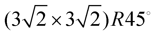 supercell (0.056 ML). supercell (0.056 ML). | ||
Regarding absolute values of di, DFT does not agree with experiment here either, perhaps for similar reasons. The experimental dH and dC, at negative voltages and lowest coverage, (Fig. 3b), are smaller by factors of roughly 5 and 9, respectively, than values from DFT with I = 1 × 10⁻³ a.u. On the other hand, the FWHM of the central protrusion is 0.38 ± 0.04 nm in experiment, in apparent agreement with DFT, which predicts 0.40–0.41 nm under the same conditions as above. (Values of FWHM from DFT are given in the ESI†).
Regarding the coverage-dependence of the di parameters, Table 2 shows values predicted for 0.04 to 0.25 ML. Here VS is small and fixed, corresponding to integrating partial charge density between limits of Ef ± 0.1 eV. Corrugation dC, apparent height dH, and the ratio dH/dC all increase as θS increases from 0.056 to 0.25 ML. In Section 3.1, the data similarly showed that dH, dC, and dH/dC are all larger for a coverage of 0.09 ML than for 0.01–0.03 ML. Essentially, the sombrero loses its dark rim, evolving toward a pure protrusion with increasing coverage, in both theory and experiment.
| Supercell | Coverage, ML | d T | d C | d H | d H /d C |
|---|---|---|---|---|---|
| (5 × 5) | 0.040 | 0.541 | 0.062 | 0.053 | 0.85 |
| (3√2 × 3√2)R45° | 0.056 | 0.538 | 0.060 | 0.046 | 0.77 |
| (4 × 4) | 0.063 | 0.537 | 0.066 | 0.058 | 0.88 |
| (2√2 × 2√2)R45° | 0.125 | 0.534 | 0.066 | 0.060 | 0.91 |
| (2 × 2) | 0.250 | 0.532 | 0.079 | 0.079 | 1.0 |
 supercell (0.056 ML) and I = 1 × 10⁻³ a.u. Effects of bias VS (in V) on dT, dC, dH (all in nm), and on dH/dC. Averaged over L = 7 to 12 as described in Section 2.2.4. Results for other values of I are given in Table S4 of the ESI
| V S, V | d T | d C | d H | d H/dC |
|---|---|---|---|---|
| −1.5 | 0.588 | 0.082 | 0.073 | 0.89 |
| −1.0 | 0.581 | 0.076 | 0.067 | 0.88 |
| −0.5 | 0.562 | 0.070 | 0.061 | 0.87 |
| 0.5 | 0.596 | 0.038 | 0.026 | 0.68 |
| 1.0 | 0.649 | 0.023 | 0.005 | 0.02 |
| 1.5 | 0.714 | 0.026 | −0.017 | −0.65 |
| 2.0 | 0.784 | 0.026 | −0.024 | −0.92 |
In summary, DFT predicts a sombrero-depression transition for this surface, provided I ≤ 1 × 10⁻³ a.u., corresponding to dT ≳ 0.5 to 0.8 nm. The point of transition is about 1 eV higher than experiment, however, and DFT fails to reproduce vertical dimensions. The lateral dimension, i.e. the FWHM of the central protrusion, agrees well between theory and experiment. DFT also reproduces qualitative changes in the sombrero shape with increasing θS.
4.2. S/Ag(110): DFT results
Fig. 8 presents the results for S/Ag(110), which again shows a transition with increasing VS. Here, 4 dark lobes first develop around a central protrusion with increasing VS. The lobes merge as the protrusion shrinks, forming a rounded-rectangle shape. The transition shifts to higher VS with increasing I, just as for S/Ag(100). This indicates again that small I (large dT) is necessary to reproduce the transition fully. Values of di are tabulated in the ESI,† and representative profiles are shown in Fig. 5(b).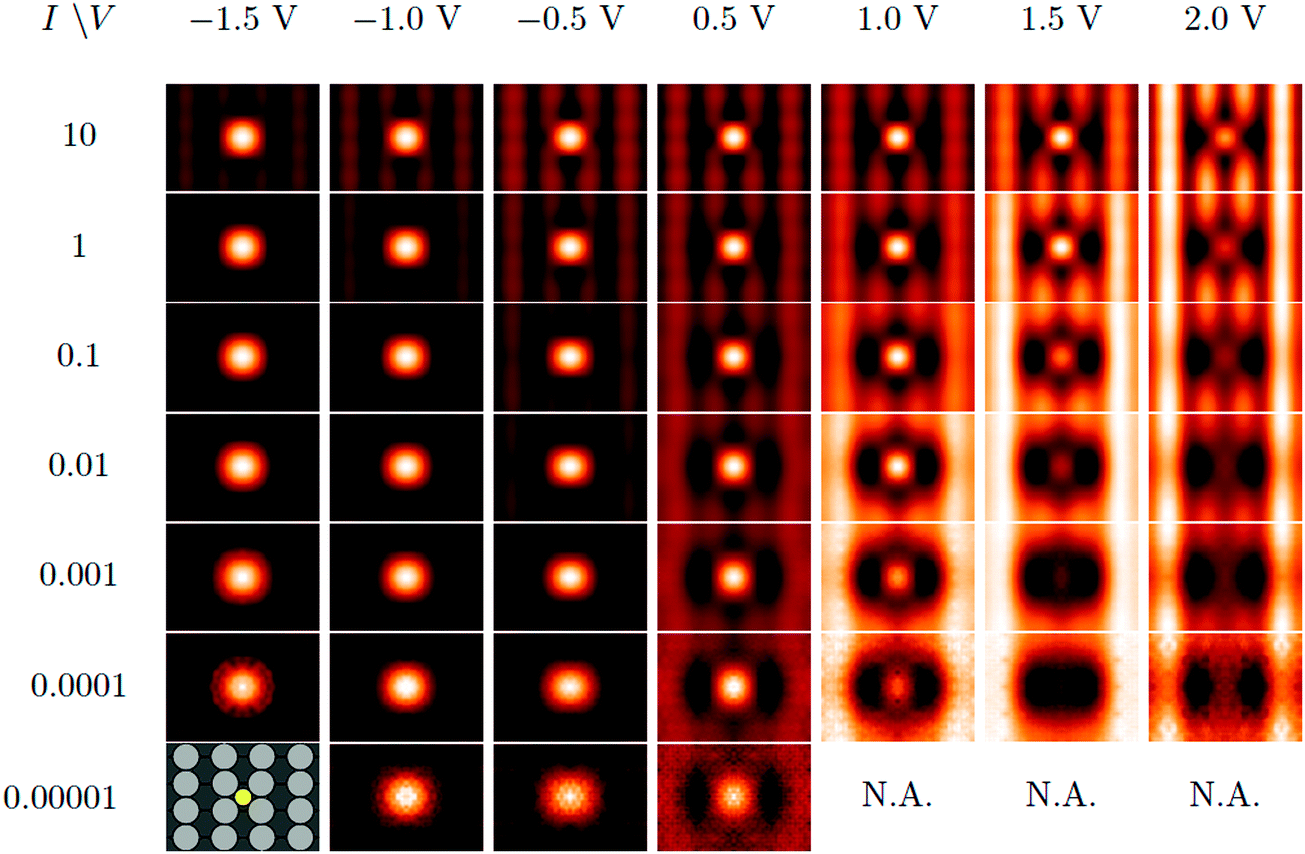 | ||
| Fig. 8 Simulated STM images of S/Ag(110) in (4 × 4) supercells (0.06 ML), with various VS and I, where I is in arbitrary units. Each image is obtained by averaging DFT calculations from L = 7 to 12, as described in Section 2.2.4. | ||
The existence of a transition from sombrero to depression, at least at low I ≤ 1 × 10⁻³ a.u., reproduces experimental observation. Furthermore, the 4 dark lobes around the central protrusion, in Fig. 8, resemble the 4 dark lobes observed in experiment in Fig. 4(c and d).
Finally, in experiment the transition from sombrero to depression occurs at higher VS on (110) than (100). However, this feature is not reproduced by DFT, which instead shows that the transition occurs at about the same VS on the two surfaces.
4.3. S/Ag(111): DFT results
Although there are no experimental data for S/Ag(111), it is enlightening to examine the DFT results. Fig. 9 shows the simulated STM images; corresponding values of di are tabulated in Table S6 of the ESI,† and profiles are shown in Fig. 5(c). At low VS and low I, dH/dC = 1, indicating a pure protrusion. For other values of VS and I, dH/dC < 1, indicating a sombrero. However, S/Ag(111) shows a fundamental difference from the (100) and (110) surfaces: No transition from sombrero to depression occurs. This is true for all values of I, indicating that the absence of transition is independent of dT at least within the range investigated. The protrusion never even dips below the surface plane, i.e. dH > 0 for all simulated images. | ||
| Fig. 9 Simulated STM images of S/Ag(111) in a (4 × 4) supercell (0.06 ML), with various bias voltage and current. Each image is obtained by averaging DFT calculations with slab thickness from L = 7 to 12 as described in Section 2.2.4. | ||
While data are unavailable for S/Ag(111), some information is available for S/Au(111). There, at low coverage, S atoms are also imaged as sombreros, but no transition to a depression occurs over −2 V ≤ VS ≤ +2 V.53,54 In fact, as predicted for Ag(111), the central protrusion never falls below the surface plane. Thus, the predictions for S/Ag(111) seem to be relevant to S/Au(111).
5. Discussion
Lowest currents, corresponding to largest sample–tip separations dT, give best agreement with experimental data, judging by the existence of the sombrero-to-depression transition within a reasonable voltage range. Best agreement for Ag(100) and Ag(110) is for I ≤ 10−3 in the arbitrary units defined herein for DFT, which corresponds to dT ≳ 0.5–0.8 nm.As mentioned in Section 2, STM images of adsorbates were first treated theoretically by Lang23,24 using the jellium model. Whether the adsorbate appears as a protrusion or depression depends on the way the adsorbate affects the local density of states. For S, the 3p peak lies more than 2 eV below the Fermi level, and thus contributes less to the tunneling current than more electropositive adsorbates such as Na at low bias. Furthermore, about 1 eV above the Fermi level, the presence of S reduces the density of states, which leads to S appearing as a depression at higher positive bias in Lang's model.
Results of Lang are in remarkable agreement with our STM experiments of S/Ag(100) and S/Ag(110), despite using a crude jellium model for the substrate. The subject was revisited by Sautet25 using Pt(111) as the substrate and studied theoretically with a tight-binding model. The tunneling current was quite usefully decomposed into through-surface and through-adsorbate contributions. The presence of an adsorbate generally caused a depression in the through-surface contribution by blocking interactions between the tip and the surface. This was counteracted by the through-adsorbate contribution. Whether the final image was a depression or a protrusion depended on the competition between the two components. In general, the through-surface depression was wider and flatter, and the through-adsorbate was narrower, thus explaining why a ring of depression can appear around a bright spot.
However, none of these treatments dealt with the effect of surface orientations. To gain more insight into the resulting STM images for S on different Ag surfaces, Fig. 10 shows the partial charge density 0.7 nm above the top layer of the substrate, along a line passing through the S adsorbate. We define a quantity that is proportional to the tunneling conduction in the extended Tersoff–Hamann method [cf.eqn (6)]
 | (8) |
 | ||
Fig. 10 Conductance at 0.7 nm above the surface, near a S atom on different Ag surfaces, at different VS. (a) S/Ag(100),  supercell. (b) S/Ag(110), (4 × 4) supercell. (c) S/Ag(111), (4 × 4) supercell. supercell. (b) S/Ag(110), (4 × 4) supercell. (c) S/Ag(111), (4 × 4) supercell. | ||
Following Sautet,25 the tunneling conductance can be separated into through-adsorbate and through-surface parts, the former being more important when the tip is directly above the adsorbate, while the latter dominates when the tip is far removed, laterally, from the adsorbate (|x| > 0.4 nm). The through-adsorbate component behaves very similarly for Ag(100) and Ag(111), increasing from 1.1(1.6) × 10−7 to 3.8(4.4) × 10−7 e Å−3 V−1 as the tunneling bias increases from −1.5 V to 2.0 V for Ag(100) [Ag(111)]. On the other hand, the through-surface contributions behave quite differently. For Ag(100), it increases from 1.3 × 10⁻⁸ to 4.4 × 10⁻⁷. For Ag(111), it increases from 1.1 × 10⁻⁸ to 1.9 × 10⁻⁷. Thus for Ag(100), the bare metal surface has a higher charge density above the Fermi level, resulting in the S appearing first as a sombrero, then a depression as bias voltage increases. For Ag(111), the through-surface contribution never increases above that of the through-adsorbate contribution, thus S always appears as a protrusion in the range of bias investigated. However, a dark ring does appear around |x| ≈ 0.4 nm. For S/Ag(110), the situation resembles S/Ag(100), especially at higher voltage, such that S appears as a depression at high VS.
It can be instructive to plot σ as a function of VS. Fig. 11(a) shows average σ values 0.7 nm above the surface (top layer Ag ions) as a function of VS for the clean Ag(100), Ag(110), and Ag(111) surfaces. For negative VS, curves for different orientations are very similar. As VS increases, σ for Ag(100) and Ag(110) increases much more quickly than for Ag(111).
 | ||
| Fig. 11 (a) Average conductance σ at 0.7 nm above the clean surface of Ag(100), Ag(110), and Ag(111) as a function of VS. (b) σ directly above the S adsorbate (dotted lines) and far away from the adsorbate (solid lines). In both panels, blue represents (100), red (110), and black (111). | ||
With the adsorption of sulfur, σ further away from the adsorbate behaves similarly to the clean surface, albeit with a lower density reflecting charge transfer from the metal to S. Those are shown as solid lines in Fig. 11(b). Directly above S, σ is more strongly influenced by the adsorbate, as shown by the dashed lines. Here, at VS < 0.5 V, the bias dependence is minimal, with σ smallest for S/Ag(110), and largest for S/Ag(111). The order is likely due the heights of the S nucleus on different surfaces, which is lowest on the open (110) and highest on the dense (111). As VS increases, σ above an adsorbed S also increases, but on Ag(100) and Ag(110), it increases less quickly than σ far from the adsorbed S, so that the STM images for S adsorbates change toward depressions. For S/Ag(111), σ directly above the S adsorbate is always larger than σ far from the S atom.
Further insights can be obtained from inspecting the local density of states of the top layer atoms on the Ag(100) and Ag(111) surfaces. In the ground state, Ag atoms have 4d105s1 electronic configuration. On Ag(100), the unoccupied s orbital (LUMO) has a peak around 3.0 eV above the Fermi level. For Ag(111), the s-like LUMO has a peak nearly 5.0 eV above the Fermi level. Thus at moderate voltage, tunneling to the empty states is much easier on the (100) than the (111) surface. For Ag(110), the s orbital seems to split into two peaks around 2 eV and 5 eV above the Fermi level. The presence of the lower state leads to an expectation that the (110) will resemble (100) more than (111), as observed.
Finally, it is interesting that our observations for S/Ag(100) are analogous to those for O/Ag(100), where the O adatom also transforms from a sombrero to a depression in STM images, at 0.5 V < VS < 0.7 V.7 Using a Green's function approach to model this behavior, the authors found that the O 2pz orbital has a rather low localized density of states at and around the Fermi level, but this is countered by a strong resonance between this orbital and the s orbital of the metal. Our present work does not contradict this interpretation, which may apply to S adatoms as well (with the O 2pz orbital replaced by the S 3pz). However, our work shows that an additional factor—through-surface tunneling—is essential to consider. It is this component that has the larger voltage dependence, rather than the through-adsorbate component.
6. Conclusions
In this paper, we have reported that S atoms on Ag(100) and Ag(110) exhibit a transition from sombrero to depression with increasing bias voltage, VS. Using a modified version of the Lang–Tersoff–Hamann method to simulate STM images, we have shown that atomistic DFT can reproduce both the shapes and the transition between them, provided that the tunneling current is relatively low, corresponding to realistic tip–sample separations. Achieving these conditions in the calculations requires sufficiently large separation (vacuum) between slabs, together with high energy cutoff, to ensure appropriate exponential decay of electron density into vacuum. We also predict that an analogous transition is not expected for S atoms on Ag(111) surfaces. Unfortunately, experimental data is not accessible for S/Ag(111), but a related system, S/Au(111), does exhibit the predicted behavior.Following Sautet,25 we have analyzed the results in terms of the through-surface conductance, which defines the metallic surface height in STM, and through-adsorbate conductance, which defines the apparent height at a point directly above the adsorbate. We have shown that both heights increase with increasing VS, but the first increases much faster than the second on Ag(100) and Ag(110), and this accounts for the observed transition on these two surfaces. On Ag(111), the two levels increase at comparable rates, so there is no transition. It is thus important to take into account the through-surface contribution when interpreting voltage-dependent images, especially when comparing different surfaces.
Conflicts of interest
There are no conflicts to declare.Acknowledgements
The experimental component of this work was conducted or supervised by PS, HW, JO, HJY, YK, and PAT. The experimental component was supported by three sources. From the U.S., experimental work was funded by NSF Grant CHE-1507223. From Japan, support was provided by a Grant-in-Aid for Scientific Research on Priority Areas “Electron Transport Through a Linked Molecule in Nano-scale”; and a Grant-in-Aid for Scientific Research(S) “Single Molecule Spectroscopy using Probe Microscope” from the Ministry of Education, Culture, Sports, Science, and Technology (MEXT). The theoretical component of this work was conducted by DJL, with support from the Division of Chemical Sciences, Basic Energy Sciences, U.S. Department of Energy (DOE). The theoretical component of the research was performed at Ames Laboratory, which is operated for the U.S. DOE by Iowa State University under contract no. DE-AC02-07CH11358. This part also utilized resources of the National Energy Research Scientific Computing Center, which is a User Facility supported by the Office of Science of the U.S. DOE under Contract No. DE-AC02-05CH11231.References
- H. Walen, D. J. Liu, J. Oh, H. J. Yang, P. M. Spurgeon, Y. Kim and P. A. Thiel, J. Phys. Chem. B, 2018, 122, 963–971 CrossRef PubMed.
- T. Duguet and P. A. Thiel, Prog. Surf. Sci., 2012, 87, 47–62 CrossRef CAS.
- T. Duguet, B. Unal, M. C. de Weerd, J. Ledieu, R. A. Ribeiro, P. C. Canfield, S. Deloudi, W. Steurer, C. J. Jenks, J. M. Dubois, V. Fournee and P. A. Thiel, Phys. Rev. B: Condens. Matter Mater. Phys., 2009, 80, 9 Search PubMed.
- J. Y. Park, D. F. Ogletree, M. Salmeron, R. A. Ribeiro, P. C. Canfield, C. J. Jenks and P. A. Thiel, Phys. Rev. B: Condens. Matter Mater. Phys., 2005, 72, 4 Search PubMed.
- J. Y. Park, G. M. Sacha, M. Enachescu, D. F. Ogletree, R. A. Ribeiro, P. C. Canfield, C. J. Jenks, P. A. Thiel, J. J. Saenz and M. Salmeron, Phys. Rev. Lett., 2005, 95, 4 Search PubMed.
- K. Morgenstern and J. Nieminen, J. Chem. Phys., 2004, 120, 10786–10791 CrossRef CAS PubMed.
- S. Schintke, S. Messerli, K. Morgenstern, J. Nieminen and W. D. Schneider, J. Chem. Phys., 2001, 114, 4206–4209 CrossRef CAS.
- L. Bartels, G. Meyer and K. H. Rieder, Appl. Phys. Lett., 1997, 71, 213–215 CrossRef CAS.
- T. B. Rawal, M. Smerieri, J. Pal, S. Hong, M. Alatalo, L. Savio, L. Vattuone, T. S. Rahman and M. Rocca, Phys. Rev. B, 2018, 98, 14 CrossRef.
- C. Zaum and K. Morgenstern, Appl. Phys. Lett., 2018, 113, 4 CrossRef.
- K. Scheil, N. Lorente, M. L. Bocquet, P. C. Hess, M. Mayor and R. Berndt, J. Phys. Chem. C, 2017, 121, 25303–25308 CrossRef CAS.
- W. H. Han, E. N. Durantini, T. A. Moore, A. L. Moore, D. Gust, P. Rez, G. Leatherman, G. R. Seely, N. J. Tao and S. M. Lindsay, J. Phys. Chem. B, 1997, 101, 10719–10725 CrossRef CAS.
- K. Comanici, F. Buchner, K. Flechtner, T. Lukasczyk, J. M. Gottfried, H. P. Steinruck and H. Marbach, Langmuir, 2008, 24, 1897–1901 CrossRef CAS PubMed.
- S. S. Ferng and D. S. Lin, J. Phys. Chem. C, 2012, 116, 3091–3096 CrossRef CAS.
- G. A. Shah, M. W. Radny, P. V. Smith, S. R. Schofield and N. J. Curson, J. Chem. Phys., 2010, 133, 4 CrossRef PubMed.
- K. Sakamoto, S. T. Jemander, G. V. Hansson and R. I. G. Uhrberg, Phys. Rev. B: Condens. Matter Mater. Phys., 2002, 65, 5 Search PubMed.
- D. F. Padowitz and R. J. Hamers, J. Phys. Chem. B, 1998, 102, 8541–8545 CrossRef CAS.
- A. Rosenhahn, J. Schneider, J. Kandler, C. Becker and K. Wandelt, Surf. Sci., 1999, 433, 705–710 CrossRef.
- A. Rosenhahn, J. Schneider, C. Becker and K. Wandelt, J. Vac. Sci. Technol., A, 2000, 18, 1923–1927 CrossRef CAS.
- T. Maroutian, S. Degen, C. Becker, K. Wandelt and R. Berndt, Phys. Rev. B: Condens. Matter Mater. Phys., 2003, 68, 5 CrossRef.
- F. Calleja, A. Arnau, J. J. Hinarejos, A. L. V. de Parga, W. A. Hofer, P. M. Echenique and R. Miranda, Phys. Rev. Lett., 2004, 92, 4 CrossRef PubMed.
- P. Sautet, J. C. Dunphy and M. Salmeron, Surf. Sci., 1996, 364, 335–344 CrossRef CAS.
- N. D. Lang, Phys. Rev. B: Condens. Matter Mater. Phys., 1986, 34, 5947–5950 CrossRef.
- N. D. Lang, Phys. Rev. Lett., 1987, 58, 45–48 CrossRef CAS PubMed.
- P. Sautet, Surf. Sci., 1997, 374, 406–417 CrossRef CAS.
- J. Nieminen, S. Lahti, S. Paavilainen and K. Morgenstern, Phys. Rev. B: Condens. Matter Mater. Phys., 2002, 66, 9 CrossRef.
- J. M. Blanco, C. Gonzalez, P. Jelinek, J. Ortega, F. Flores, R. Perez, M. Rose, M. Salmeron, J. Mendez, J. Wintterlin and G. Ertl, Phys. Rev. B: Condens. Matter Mater. Phys., 2005, 71, 4 CrossRef.
- S. M. Russell, Y. Kim, D. J. Liu, J. W. Evans and P. A. Thiel, J. Chem. Phys., 2013, 138, 4 CrossRef PubMed.
- H. Walen, D. J. Liu, J. Oh, H. Lim, J. W. Evans, Y. Kim and P. A. Thiel, J. Chem. Phys., 2015, 142, 14 CrossRef PubMed.
- H. Walen, D. J. Liu, J. Oh, H. Lim, J. W. Evans, C. M. Aikens, Y. Kim and P. A. Thiel, Phys. Rev. B: Condens. Matter Mater. Phys., 2015, 91, 7 CrossRef.
- P. Zeppenfeld, C. P. Lutz and D. M. Eigler, Ultramicroscopy, 1992, 42, 128–133 CrossRef.
- J. A. Stroscio and D. M. Eigler, Science, 1991, 254, 1319–1326 CrossRef CAS PubMed.
- P. Sautet and M. L. Bocquet, Surf. Sci., 1994, 304, L445–L450 CrossRef CAS.
- P. Sautet and M. L. Bocquet, Phys. Rev. B: Condens. Matter Mater. Phys., 1996, 53, 4910–4925 CrossRef CAS.
- M. A. VanHove, J. Cerda, P. Sautet, M. L. Bocquet and M. Salmeron, Prog. Surf. Sci., 1997, 54, 315–329 CrossRef CAS.
- A. Gustafsson, N. Okabayashi, A. Peronio, F. J. Giessibl and M. Paulsson, Phys. Rev. B, 2017, 96, 8 CrossRef.
- C. Wagner, J. Chem. Phys., 1953, 21, 1819–1827 CrossRef CAS.
- D. Detry, J. Drowart, P. Goldfinger, H. Keller and H. Rickert, Z. Phys. Chem., 1967, 55, 314–319 CrossRef CAS.
- W. Heegemann, K. H. Meister, E. Bechtold and K. Hayek, Surf. Sci., 1975, 49, 161–180 CrossRef CAS.
- J. Bardeen, Phys. Rev. Lett., 1961, 6, 57 CrossRef CAS.
- J. M. Blanco, F. Flores and R. Perez, Prog. Surf. Sci., 2006, 81, 403–443 CrossRef CAS.
- J. Tersoff and D. R. Hamann, Phys. Rev. B: Condens. Matter Mater. Phys., 1985, 31, 805–813 CrossRef CAS.
- G. Kresse and J. Furthmuller, Phys. Rev. B: Condens. Matter Mater. Phys., 1996, 54, 11169–11186 CrossRef CAS.
- J. P. Perdew, K. Burke and M. Ernzerhof, Phys. Rev. Lett., 1996, 77, 3865–3868 CrossRef CAS PubMed.
- J. P. Perdew, K. Burke and M. Ernzerhof, Phys. Rev. Lett., 1997, 78, 1396 CrossRef CAS.
- P. E. Blochl, Phys. Rev. B: Condens. Matter Mater. Phys., 1994, 50, 17953–17979 CrossRef.
- C. J. Chen, Introduction to Scanning Tunneling Microcopy, Oxford University Press, 1993 Search PubMed.
- Y. Han and D. J. Liu, Phys. Rev. B: Condens. Matter Mater. Phys., 2009, 80, 17 Search PubMed.
- D. J. Liu, Phys. Rev. B: Condens. Matter Mater. Phys., 2010, 81, 10 Search PubMed.
- Z. Liang, H. J. Yang, Y. Kim and M. Trenary, J. Chem. Phys., 2014, 140, 6 Search PubMed.
- C. Y. Qin and J. L. Whitten, Surf. Sci., 2005, 588, 83–91 CrossRef CAS.
- P. Sautet, Chem. Rev., 1997, 97, 1097–1116 CrossRef CAS.
- H. Walen, D. J. Liu, J. Oh, H. Lim, J. W. Evans, Y. Kim and P. A. Thiel, J. Chem. Phys., 2015, 143, 10 CrossRef PubMed.
- H. Walen, PhD thesis, Iowa State University, 2016.
Footnotes |
| † Electronic supplementary information (ESI) available. See DOI: 10.1039/c9cp01626k |
| ‡ Present address: Space Dynamics Laboratory, 1695 Research Park Way, North Logan, Utah 84341, USA. |
| § Present address: Fritz Haber Institute of the Max Planck Society, Faradayweg 4, 14195 Berlin, Germany. |
| This journal is © the Owner Societies 2019 |