
 Open Access Article
 This Open Access Article is licensed under a Creative Commons Attribution-Non Commercial 3.0 Unported Licence
Destructive role of oxygen in growth of molybdenum disulfide determined by secondary ion mass spectrometry
Paweł Piotr
Michałowski
 *,
Piotr
Knyps
,
Paweł
Ciepielewski
,
Piotr
Caban
,
Ewa
Dumiszewska
and
Jacek
Baranowski
*,
Piotr
Knyps
,
Paweł
Ciepielewski
,
Piotr
Caban
,
Ewa
Dumiszewska
and
Jacek
Baranowski
Institute of Electronic Materials Technology, Wólczyńska 133, 01-919 Warsaw, Poland. E-mail: pawel.michalowski@itme.edu.pl
First published on 3rd April 2019
Abstract
The application of secondary ion mass spectrometry (SIMS) in investigation and comparison of molybdenum disulfide (MoS2) films grown on SiO2, Al2O3 and BN substrates is presented. SIMS measurements of the MoS2/substrate interface reveals oxygen out-diffusion from the substrates containing oxygen and the formation of an amorphous MoOS layer in addition to MoS2. The total area of MoS2 domains covering the substrate is directly related to the type of substrate. For SiO2, small triangular domains of MoS2 separated by amorphous MoOS material are observed. For Al2O3, the sizes of the MoS2 domains are drastically improved due to the higher stability of sapphire. For a BN substrate, SIMS measurements reveal a uniform MoS2 coverage over the whole 2-inch wafer. These results show the destructive role of oxygen released from substrates such as SiO2 or Al2O3 during the growth process of MoS2. The fast and cheap growth process on a non-oxide substrate allows large wafer-scale uniform molybdenum disulfide material to be obtained, which is promising for device fabrication.
1 Introduction
Two-dimensional transition metal dichalcogenides (TMDs), such as MoS2, MoSe2, WS2, WSe2etc. have received great attention and have emerged as an attractive class of nano-materials due to their unique structures.1–4 Their electronic properties vary with thickness and make them possible candidates for 2D nano-electronic and optoelectronic applications such as solar cells, photodetectors, field effect transistors, and sensors.Among TMD materials, molybdenum disulfide has been extensively studied.5–13 MoS2 is a two-dimensional crystal with strong in-plane covalent bonding and weak out of plane van der Waals interactions. In the monolayer form, MoS2 has a direct energy gap.
The most common way to obtain MoS2 monolayers is by mechanical exfoliation of bulk material. However, this method is not promising for obtaining large wafer-scale uniform areas of 2D material suitable for device fabrication. There have been several attempts to produce MoS2 layers via chemical vapour deposition (CVD) on insulating substrates.14–16 Among CVD methods, the direct growth of 2D materials with the use of thin metal film deposition connected with controlled sulfurization has become one of the promising ways to synthesize large area 2D materials.17,18 In the present work, we report successful sulfurization of molybdenum film deposited on different substrates such as SiO2, Al2O3 and BN.
Various experimental techniques such as Raman spectroscopy, transmission electron microscopy, scanning probe microscopy, scanning tunnelling microscopy, atomic force microscopy, X-ray diffraction, and X-ray photoelectron spectroscopy have been used to investigate 2D materials.19–30 Each of these methods has its own strengths and limitations, and the information they provide is complementary. In this work, secondary ion mass spectrometry (SIMS) is introduced as a suitable method for characterization of MoS2 layers. The technique is widely used to determine the elemental composition of a sample,31–36 however in the case of 2D materials sub-nanometer depth resolution is required. In our previous works we have already established reliable procedures to characterize such samples, namely graphene37–41 and boron nitride.42,43 These results have inspired us to methodically develop our measurement procedures and adjust them for a wide range of 2D materials, including MoS2.
The main motivation of this work is to investigate the role of substrates such as SiO2, Al2O3 and BN on the quality and size of the grown MoS2 domains. The SIMS measurements play an essential role in this investigation. It is shown that the choice of substrate has a dramatic influence on the size of the grown MoS2 domains.
2 Experimental
2.1 Sample preparation
Three kinds of substrate were used for the growth of MoS2 layers:1. Sample A: SiO2/Si (thermal oxide of 200 nm of SiO2 on a Si substrate)
2. Sample B: sapphire (Al2O3)
3. Sample C: BN grown on Al2O3
The sizes of all substrates were 2 inches. Boron nitride was grown at 1050 °C in the self-terminated growth mode, which corresponds to a thickness of 2 nm by the CVD process described by us previously.42 All samples were cleaned in alcohol and DI water. Thin Mo film deposition was done by an e-beam PVD deposition process. Deposition of Mo metal was done under 5 × 10⁻⁷ Torr pressure with a rate of 0.05 Å s−1. The evaporated Mo film had from 0.4 to 1.0 nm thickness. The Mo sputtered samples were placed in the high temperature zone of a chemical vapour deposition (CVD) reactor for sulfurization to form MoS2 film. H2S was used as the source of sulfur and H2 as the carrier gas. The furnace was heated up to a temperature of 750 °C and held for 15 minutes. Afterwards, the growth furnace was naturally cooled to 150 °C for evaporation of excess sulfur from the surface of the samples. A monolayer of MoS2 exfoliated from a bulk material and transferred on to SiO2 was used as a reference sample.
2.2 SIMS measurements
In this work, all SIMS measurements were performed employing a CAMECA SC Ultra instrument under ultra-high vacuum (UHV), usually of 4 × 10⁻¹⁰ mbar. The Cs+ primary beam was rastered over 80 × 80 μm2 (the analysis area was limited to 50 × 50 μm2) and positive ions detection mode was used in the experiments and thus all species were measured as CsX+ cluster ions. The intensity of the primary beam was 4 nA and the impact energy was 150 eV. For precise oxygen detection measurements, secondary ions detection mode was switched to negative but the rest of the parameters remained the same. To avoid charging problems the electron gun was used. A highly uniform beam was required for this work – the beam on the sample in the SC Ultra tool has a square shape and owning to the “variable rectangular shape concept” forms a homogeneous spot. The primary beam at the working point in the SC Ultra is formed by two stencils – well-shaped apertures. While the first one is used to choose the most intense and homogeneous part of the Gaussian-shaped ion beam, the second one changes the size of the spot. This innovation provides high sensitivity for all measured elements.44–46The lateral imaging mode was very important in these experiments. This task was, however, very challenging. The intensity of SIMS signals in the CsX+ mode depended predominantly on cesium deposition at the surface of the sample. In the depth profiling mode, ions were collected from a large area and thus the average intensity was very stable. For the imaging mode each point was measured individually and thus some significant fluctuations might decrease the quality of measurements. Indeed, we performed standard imaging measurements on the reference sample – see Fig. 1A – and found that while the average ratio of the Mo and S signals was 4.313 (just like it was in the depth profiling mode), the fluctuations were as high as 30%. It was concluded that a proper identification of the MoS2 phase would be impossible for this kind of experiment.
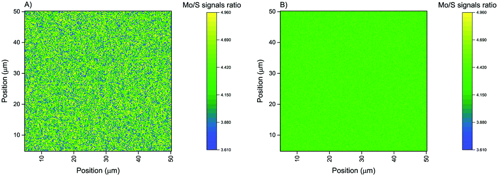 | ||
| Fig. 1 SIMS distribution maps for the reference sample. (A) The standard imaging procedure showed significant fluctuations; (B) the refined procedure increases the quality of measurements and is suitable for identification of the MoS2 phase. | ||
To solve this issue, the source of these fluctuations was identified. The primary beam was very uniform and thus a lateral distribution of cesium at the surface of a sample should have inherited this characteristic. The problem was that the magnetic sector SIMS can only measure one ion at a time. In the depth profiling mode, it was not an important issue as the integration time for each signal was about one second, so each cycle was as follows: integration of the S signal, adjusting the electromagnet for different ion mass (during this phase the primary beam was blanked and the sample was not sputtered), integration of the Mo signal and once again adjusting the electromagnet. It meant that there was only one second of sputtering time difference between the integration of the S and Mo signals, and thus it was not expected that the cesium deposition changed significantly within that time. Such a short integration time could be used because ions were collected from a relatively large area. Lateral imaging, however, required much longer integration time to achieve similar sensitivity – in this particular case each signal was integrated for fifteen seconds to form a distribution map. During that time the cesium deposition might have changed a lot and thus the Mo/S ratio fluctuated a lot. To solve this problem we changed the measurement procedure: each signal was sequentially integrated for about 0.3 seconds and fifty cycles were summed to form a distribution map so that the total integration time of each signal was fifteen seconds. Such a procedure is significantly more time consuming as it introduced fifty times more electromagnet adjusting phases (each of them lasted for about two seconds) during which the sample was not sputtered, but it increased the quality of measurements. Indeed, measurements on the reference sample with this refined procedure – see Fig. 1B – showed that the fluctuations were reduced to about 6% which was acceptable for identification of molybdenum disulfide. Based on these results, we assumed that the ratio Mo/S = 4.313 ± 3% was a marker of the MoS2 phase.
2.3 Raman spectroscopy measurements
Room temperature Raman measurements were performed with a Renishaw inVia Raman microscope using a 532 nm wavelength obtained from a Nd:YAG laser. The size of a laser spot was about 0.5 μm and the power was below 0.1 mW to avoid the destruction of MoS2 layers. The laser was focused on the sample using a ×100 objective and numerical aperture NA = 0.9 in a backscattering geometry.3 Results & discussion
When a new growth procedure is being established and optimized it is usually advisable to test it on a cheap, easily accessible substrate. The growth of MoS2 films on SiO2 substrates meets this criterion and provides the additional advantage of possible direct integration of a novel 2D material with the existing silicon-based fabrication lines. However, the influence of the substrate on the growth process is often omitted. The SIMS imaging mode shows that the quality of the obtained film is poor – Fig. 2A and B presents lateral distributions of the Mo/S ratio close to the surface and the substrate, respectively. As was determined on a reference sample, the ratio of Mo/S signals equals 4.313 for MoS2 material. It can be immediately noted that the proposed measurement procedure is effective as triangles of molybdenum disulfide can be identified, and this material is particularly known for formation of such triangular domains.47–50 Experiments performed on several different spots confirmed that for layers closer to the surface the size of the MoS2 domains is bigger. | ||
| Fig. 2 SIMS distribution maps for sample A. Maps (A) and (B) show the Mo/S distribution close to the surface and the substrate, respectively (counting from the surface) while (C) and (D) show oxygen distribution for the same layers. Bigger domains are formed close to the surface. | ||
Outside of these triangular domains, the ratio of Mo/S signals is chaotic but the average value is below 4.313. Some points are close to this value, but it should be noted that the lateral resolution of the experiment is about one micron and thus these points should not be treated as very small domains of MoS2. The only valid conclusion is that these regions contain more sulfur than molybdenum disulfide. To gather more information we have checked whether some other elements are present in this region. Our analysis – see Fig. 2C and D – reveals that these regions are oxidized. It should be noted that the CsX+ mode is not sensitive for oxygen contamination – when some oxygen counts are registered it can be concluded that these regions contain at least several atomic percent of this element. The lateral resolution of this element is worse than in the case of Mo and S, as oxygen ions are lighter and thus have a broader energy distribution and it is more difficult to effectively filter ions coming from neighboring regions. Nevertheless, the quality is good enough to show that no/little oxygen is found in the triangular MoS2 domains, which is particularly well visible for bigger triangles.
At this point, we were not able to determine what the source of oxygen that has oxidized the sample was. In theory, the film could have oxidized during the time it was transferred from the reactor to the SIMS tool. Thus, we decided to compare the quality of MoS2 film grown under the same growth conditions but on a different substrate. For that, we chose another easily accessible substrate, namely sapphire, and found that the quality of MoS2 films significantly increased. Fig. 3A shows the distribution of the Mo/S ratio for sample B. There is no difference between the region close to the surface and to the substrate – they look exactly the same. Even though the film is not perfectly uniform, the domains of MoS2 cover more than 90% of the sample. Boundaries between these domains contain more sulfur and are oxidized – see Fig. 3B. However, it should be noted that the width of these boundaries is artificially stretched, since when the primary beam is located partially on a MoS2 region and partially on the boundary the registered Mo/S ratio will be lower, and the whole region will be marked as molybdenum sulfide with unknown stoichiometry. Given that the average width of these boundaries is about 2–2.5 micron and the size of a primary beam is about 0.9 micron, it can be concluded that the actual width of the boundaries is in the range of 200–700 nm.
 | ||
| Fig. 3 SIMS distribution maps for sample B. Map (A) shows Mo/S and (B) shows oxygen distribution. | ||
Another possibility is that residual water present at the surface of the samples is responsible for oxidation of the molybdenum sulfide film. We have prepared several samples grown on both types of substrate but with varying vacuum annealing conditions (temperature, time) but no differences have been found. It is important to emphasize that the only difference between samples A and B is the type of substrate. The growth conditions and transfer time from the reactor to the SIMS tool have been as similar as possible. Therefore, this result reveals that the substrate itself has a crucial impact on the quality of the molybdenum sulfide film. It is not surprising that the quality of MoS2 film is much better for sapphire, as this oxide is more stable. The only remaining question is at which point of the growth procedure is oxygen from the substrate incorporated into the molybdenum sulfide film. To answer this question, we have performed additional depth profiling experiments in the negative mode which is more suitable for oxygen detection. For each type of substrate we have compared three different samples: pure substrate, Mo film before the sulfurization process and molybdenum sulfide film. Mo film is not interesting – there is some residual oxygen (in the range of ppm) but no impact of the substrate can be detected. Molybdenum sulfide film is by far more interesting. Fig. 4 presents the results of these experiments – as it has been confirmed before, a lot of oxygen can be detected in these samples but the most important finding is the interface region: it can be clearly seen that, after sputtering the whole molybdenum sulfide film, the oxygen signal is still below the level which is typical for the substrate, which means that several nanometers of the substrate is oxygen depleted. It can be therefore concluded that during the sulfurization process at 750 °C some oxygen is released from the substrate and incorporated into the film, decreasing the overall quality of the sample. We have performed additional experiments where Mo film is heated in a CVD reactor but without introduction of H2S, and oxygen depletion in the substrate has been also found (similarly to what is presented in Fig. 4). This means that at high temperature Mo atoms have a tendency to absorb oxygen from a substrate.
 | ||
| Fig. 4 Oxygen profiles for MoS2 films grown on SiO2 and Al2O3. The oxygen profiles are similar for both substrates: a clear oxygen depletion from the interface region inside of the substrates is observed. The location of the interface between MoS2 and the substrates has been identified at the point where Si or Al signals increase rapidly (these SIMS signals are not presented in the figure to achieve a better visibility). | ||
It was therefore deemed beneficial to repeat these experiments for another substrate which does not contain any oxygen, namely boron nitride. Fig. 5 presents a lateral imaging of the Mo/S ratio for a molybdenum sulfide film grown on a BN/Al2O3 substrate (sample C). It becomes immediately apparent that the film is very uniform and the quality is comparable to the reference sample (see Fig. 1B). Furthermore, no oxygen can be detected in this sample. We have repeated these measurements on 40 spots over the whole 2-inch sample. In all these areas the uniform MoS2 film has been detected without any exception. Therefore it can be concluded that the whole area of the 2-inch BN/Al2O3 substrate is covered by MoS2 film.
 | ||
| Fig. 5 SIMS distribution map for sample C. The map shows the Mo/S distribution. The sample is very uniform and can be identified as stoichiometric MoS2. | ||
Finally, we confirmed the quality of these samples with Raman spectroscopy, a powerful nondestructive characterization tool which is widely used to characterize 2D materials. Specifically, in the case of ultrathin MoS2 it is used to identify the number of layers, as it has been demonstrated by Li et al.51 that the frequencies of the Raman E12g and A1g peaks are strongly dependent on the MoS2 thickness in the range of 1–4 monolayers. The frequency difference of these modes increases from about 19 cm−1 for a monolayer to 25 cm−1 for a bulk material.
Fig. 6 compares the Raman spectra of samples A, B and C. It can be immediately noted that the quality of the sample A is poor – both peaks are broad and of very low intensity (the Raman signal was collected 5 times longer with the same laser power). The frequency difference is about 24 cm−1 which indicates four layers of MoS2. Sample B is of much better quality. Both peaks are sharp and intense. The frequency difference is about 22 cm−1 which indicates two layers of MoS2. Sample C is confirmed to be of the highest quality, and the frequency difference is about 23 cm−1 which indicates three layers. The map of the frequency difference between E12g and A1g peaks indicates that the average thickness of the MoS2 film is uniform indeed.
 | ||
| Fig. 6 Raman spectra of samples A, B and C. Changing the substrate from silicon dioxide to sapphire significantly increased the quality of the MoS2, but the sample grown on boron nitride was the best one. The Raman map shows the energy difference between the E12g and A1g peaks for sample C. | ||
4 Conclusions
The most important result of our investigation is a comparison of the MoS2 coverage area on different types of substrates. It has been found that the coverage is dramatically influenced by the choice of type of substrate, such as SiO2, Al2O3, or BN. SIMS measurements have revealed the release of oxygen from a substrate such as SiO2 or Al2O3, which has a drastic influence on the size of the grown MoS2 domains. During the sulfurization of Mo, the oxygen out-diffuses from a substrate and reacts with Mo, leading to formation of an amorphous MoOS material of unknown stoichiometry. In the case of growth on a SiO2 substrate, a relatively large amount of oxygen was released, leading to the formation of a large area of amorphous MoOS covering about 50% of the total area. The presence of MoOS prevented enlargement of the MoS2 triangle domains. On the other hand, sapphire is a much more stable oxide then SiO2 and, therefore, a smaller amount of oxygen may go into the grown layer, which led to much larger MoS2 domains separated by narrow oxidized boundaries. In this case, about 90% of the whole area was covered by MoS2 domains and only 10% by oxygen-rich amorphous MoOS. Some substrates such as BN do not contain oxygen at all. The BN layer grown on Al2O3 separates the sapphire, and apparently blocks oxygen diffusion to the grown MoS2 film. In this case, 100% of the BN 2-inch wafer was covered by continuous and uniform MoS2.Let us emphasize the key role of SIMS measurements in our investigation. SIMS determination of the presence of oxygen at the MoS2/substrate interface has disclosed the process of oxygen out-diffusing from oxide substrates. This process is destructive from the perspective of growth of MoS2 domains, due to the formation of MoOS material which prohibits the formation of a large and continuous MoS2 film. The BN substrate, being free from oxygen, is the optimal one for obtaining continuous wafer-scale MoS2 film.
Generalizing, the presented SIMS results show the invalidity of the assumption that a substrate does not react with a grown layer in CVD growth. Such a reaction can go beyond simple contamination and can determine the size of the grown MoS2 domains. The choice of an oxide-free substrate for the growth of MoS2, and most likely for other TMDs, is of fundamental importance especially when device fabrication is considered.
Conflicts of interest
There are no conflicts to declare.Acknowledgements
This work was supported by the European Union's Horizon 2020 research and innovation programme under grant agreement no. 785219.References
- W. S. Yun, S. W. Han, S. C. Hong, I. G. Kim and J. D. Lee, Phys. Rev. B: Condens. Matter Mater. Phys., 2012, 85, 033305 CrossRef.
- D. W. Bullett, J. Phys. C: Solid State Phys., 1978, 11, 4501 CrossRef CAS.
- Q. H. Wang, K. Kalantar-Zadeh, A. Kis, J. N. Coleman and M. S. Strano, Nat. Nanotechnol., 2012, 7, 669 Search PubMed.
- X. Song, J. Hu and H. Zeng, J. Mater. Chem. C, 2013, 1, 2952 RSC.
- S. Ding, D. Zhang, J. S. Chen and X. W. D. Lou, Nanoscale, 2012, 4, 95 RSC.
- Y. Li, H. Wang, L. Xie, Y. Liang, G. Hong and H. Dai, J. Am. Chem. Soc., 2011, 133, 7296 CrossRef CAS PubMed.
- G. L. Yu, R. Jalil, B. Belle, A. S. Mayorov, P. Blake, F. Schedin, S. V. Morozov, L. A. Ponomarenko, F. Chiappini, S. Wiedmann, U. Zeitler, M. I. Katsnelson, A. K. Geim, K. S. Novoselov and D. C. Elias, Proc. Natl. Acad. Sci. U. S. A., 2013, 110, 3282 CrossRef CAS PubMed.
- S. Wi, H. Kim, M. Chen, H. Nam, L. J. Guo, E. Meyhofer and X. Liang, ACS Nano, 2014, 8, 5270 CrossRef CAS PubMed.
- A. K. Geim and I. V. Grigorieva, Nature, 2013, 499, 419 CrossRef CAS PubMed.
- M. Chhowalla, H. Shin, G. Eda, L.-J. Li, K. Loh and H. Zhang, Nat. Chem., 2013, 5, 263 CrossRef PubMed.
- W. Wu, L. Wang, Y. Li, F. Zhang, L. Lin, S. Niu, D. Chenet, X. Zhang, Y. Hao, T. Heinz, J. Hone and Z. Wang, Nature, 2014, 514, 470 CrossRef CAS PubMed.
- R. Ganatra and Q. Zhang, ACS Nano, 2014, 8, 4074 CrossRef CAS PubMed.
- X. Li and H. Zhu, J. Materiomics, 2015, 1, 33 CrossRef.
- X. Wang, H. Feng, Y. Wu and L. Jiao, J. Am. Chem. Soc., 2013, 135, 5304 CrossRef CAS PubMed.
- Y.-H. Lee, X.-Q. Zhang, W. Zhang, M.-T. Chang, C.-T. Lin, K.-D. Chang, Y.-C. Yu, J. T.-W. Wang, C.-S. Chang, L.-J. Li and T.-W. Lin, Adv. Mater., 2012, 24, 2320 CrossRef CAS PubMed.
- Y. Zhan, Z. Liu, S. Najmaei, P. M. Ajayan and J. Lou, Small, 2012, 8, 966 CrossRef CAS PubMed.
- M. H. Heyne, D. Chiappe, J. Meersschaut, T. Nuytten, T. Conard, H. Bender, C. Huyghebaert, I. P. Radu, M. Caymax, J.-F. de Marneffe, E. C. Neyts and S. De Gendt, J. Mater. Chem. C, 2016, 4, 1295 RSC.
- A. Stesmans, S. Iacovo, D. Chiappe, I. Radu, C. Huyghebaert, S. De Gendt and V. V. Afanas'ev, Nanoscale Res. Lett., 2017, 12, 283 CrossRef CAS PubMed.
- L. Malard, M. Pimenta, G. Dresselhaus and M. Dresselhaus, Phys. Rep., 2009, 473, 51 CrossRef CAS.
- G. Plechinger, S. Heydrich, J. Eroms, D. Weiss, C. Schüller and T. Korn, Appl. Phys. Lett., 2012, 101, 101906 CrossRef.
- A. Ferrari and D. Basko, Nat. Nanotechnol., 2013, 8, 235 CrossRef CAS PubMed.
- X. Ming, Int. J. Spectrosc., 2018, 2018, 4861472 Search PubMed.
- M. Paillet, R. Parret, J.-L. Sauvajol and P. Colomban, J. Raman Spectrosc., 2018, 49, 8 CrossRef CAS.
- S. Zhang, N. Zhang, Y. Zhao, T. Cheng, X. Li, R. Feng, H. Xu, Z. Liu, J. Zhang and L. Tong, Chem. Soc. Rev., 2018, 47, 3217 RSC.
- F. Liang, H. Xu, X. Wu, C. Wang, C. Luo and J. Zhang, Chin. Phys. B, 2018, 27, 037802 CrossRef.
- C. N. R. Rao and A. Nag, Eur. J. Inorg. Chem., 2015, 4244 Search PubMed.
- S. Z. Butler, S. M. Hollen, L. Cao, Y. Cui, J. A. Gupta, H. R. Gutiérrez, T. F. Heinz, S. S. Hong, J. Huang, A. F. Ismach, E. Johnston-Halperin, M. Kuno, V. V. Plashnitsa, R. D. Robinson, R. S. Ruoff, S. Salahuddin, J. Shan, L. Shi, M. G. Spencer, M. Terrones, W. Windl and J. E. Goldberger, ACS Nano, 2013, 7, 2898 CrossRef CAS PubMed.
- C. N. R. Rao, H. S. S. Ramakrishna Matte and U. Maitra, Angew. Chem., Int. Ed., 2013, 52, 13162 CrossRef CAS PubMed.
- G. R. Bhimanapati, Z. Lin, V. Meunier, Y. Jung, J. Cha, S. Das, D. Xiao, Y. Son, M. S. Strano, V. R. Cooper, L. Liang, S. G. Louie, E. Ringe, W. Zhou, S. S. Kim, R. R. Naik, B. G. Sumpter, H. Terrones, F. Xia, Y. Wang, J. Zhu, D. Akinwande, N. Alem, J. A. Schuller, R. E. Schaak, M. Terrones and J. A. Robinson, ACS Nano, 2015, 9, 11509 CrossRef CAS PubMed.
- C. Rao and U. Maitra, Annu. Rev. Mater. Res., 2015, 45, 29 CrossRef CAS.
- C. A. Andersen and J. R. Hinthorne, Science, 1972, 175, 853 CrossRef CAS PubMed.
- A. Benninghoven, Surf. Sci., 1975, 53, 596 CrossRef CAS.
- A. Benninghoven, F. G. Rudenauer and H. W. Werner, Secondary ion mass spectrometry: basic concepts, instrumental aspects, applications and trends, John Wiley & Sons, New York, 1987 Search PubMed.
- H. W. Werner, Surf. Sci., 1975, 47, 301 CrossRef CAS.
- H. Liebl, J. Vac. Sci. Technol., A, 1975, 12, 385 CrossRef CAS.
- H. Liebl, J. Appl. Phys., 1967, 38, 5277 CrossRef CAS.
- P. P. Michałowski, W. Kaszub, A. Merkulov and W. Strupinski, Appl. Phys. Lett., 2016, 109, 011904 CrossRef.
- P. P. Michałowski, W. Kaszub, I. Pasternak and W. Strupinski, Sci. Rep., 2017, 7, 7479 CrossRef PubMed.
- P. P. Michałowski, I. Pasternak and W. Strupinski, Nanotechnology, 2018, 29, 015702 CrossRef PubMed.
- P. P. Michałowski, I. Pasternak, P. Ciepielewski, F. Guinea and W. Strupinski, Nanotechnology, 2018, 29, 305302 CrossRef PubMed.
- J. Grzonka, I. Pasternak, P. P. Michałowski, V. Kolkovsky and W. Strupinski, Appl. Surf. Sci., 2018, 447, 582 CrossRef CAS.
- P. A. Caban, D. Teklinska, P. P. Michalowski, J. Gaca, M. Wojcik, J. Grzonka, P. Ciepielewski, M. Mozdzonek and J. M. Baranowski, J. Cryst. Growth, 2018, 498, 71 CrossRef CAS.
- P. P. Michałowski, P. Caban and J. Baranowski, J. Anal. At. Spectrom., 2019 10.1039/C9JA00004F.
- CAMECA, Genneviliers, CAMECA SC-Ultra, User's Guide, 2005.
- D. Kouzminov, A. Merkulov, E. Arevalo and H. J. Grossmann, Surf. Interface Anal., 2013, 45, 345 CrossRef CAS.
- A. Merkulov, Surf. Interface Anal., 2013, 45, 90 CrossRef CAS.
- R. Ionescu, W. Wang, Y. Chai, Z. Mutlu, I. Ruiz, Z. Favors, D. Wickramaratne, M. Neupane, L. Zavala, R. Lake, M. Ozkan and C. S. Ozkan, IEEE Trans. Nanotechnol., 2014, 13, 749 CAS.
- Z. Lin, M. T. Thee, A. L. Elías, S. Feng, C. Zhou, K. Fujisawa, N. Perea-López, V. Carozo, H. Terrones and M. Terrones, APL Mater., 2014, 2, 092514 CrossRef.
- W. Chen, J. Zhao, J. Zhang, L. Gu, Z. Yang, X. Li, H. Yu, X. Zhu, R. Yang, D. Shi, X. Lin, J. Guo, X. Bai and G. Zhang, J. Am. Chem. Soc., 2015, 137, 15632 CrossRef CAS PubMed.
- Z. Cheng, M. Xia, R. Hu, C. Liang, G. Liang and S. Zhang, J. Cryst. Growth, 2017, 480, 6 CrossRef CAS.
- H. Li, Q. Zhang, C. C. R. Yap, B. K. Tay, T. H. T. Edwin, A. Olivier and D. Baillargeat, Adv. Funct. Mater., 2012, 22, 1385 CrossRef CAS.
| This journal is © the Owner Societies 2019 |