
 Open Access Article
 This Open Access Article is licensed under a Creative Commons Attribution-Non Commercial 3.0 Unported Licence
A tool box to ascertain the nature of doping and photoresponse in single-walled carbon nanotubes†
Ana
Santidrián
 *ab,
José M.
González-Domínguez
bc,
Valentin
Diez-Cabanes
d,
Javier
Hernández-Ferrer
b,
Wolfgang K.
Maser
b,
Ana M.
Benito
b,
Alejandro
Anśon-Casaos
b,
Jérôme
Cornil
d,
Tatiana
Da Ros
d and
Martin
Kalbáč
*a
*ab,
José M.
González-Domínguez
bc,
Valentin
Diez-Cabanes
d,
Javier
Hernández-Ferrer
b,
Wolfgang K.
Maser
b,
Ana M.
Benito
b,
Alejandro
Anśon-Casaos
b,
Jérôme
Cornil
d,
Tatiana
Da Ros
d and
Martin
Kalbáč
*a
aJ. Heyrovský Institute of Physical Chemistry, Academy of Sciences of the Czech Republic, Dolejskova 3, 18223 Prague 8, Czech Republic. E-mail: martin.kalbac@jh-inst.cas.cz
bInstituto de Carboquímica ICB-CSIC, Miguel Luesma Castan 4, 50018 Zaragoza, Spain. E-mail: asantidrian@icb.csic.es
cINSTM Unit of Trieste, Department of Chemical and Pharmaceutical Sciences, University of Trieste, Via Licio Giorgieri 1, 34127 Trieste, Italy
dUniversity of Mons, Place du Parc 20, 7000 Mons, Belgium
First published on 23rd January 2019
Abstract
The effect of doping on the electronic properties in bulk single-walled carbon nanotube (SWCNT) samples is studied for the first time using a new in situ Raman spectroelectrochemical method, and further verified by DFT calculations and photoresponse. We use p-/n-doped SWCNTs prepared by diazonium reactions as a versatile chemical strategy to control the SWCNT behavior. The measured and calculated data testify an acceptor effect of 4-aminobenzenesulfonic acid (p-doping), and a donor effect (n-doping) in the case of benzyl alcohol. In addition, pristine and covalently functionalized SWCNTs were used for the preparation of photoactive film electrodes. The photocathodic current in the photoelectrochemical cell is consistently modulated by the doping group. These results validate the in situ Raman spectroelectrochemistry as a unique tool box for predicting the electronic properties of functionalized SWCNTs in the form of thin films and their operational functionality in thin film devices for future optoelectronic applications.
Introduction
In the last few decades, unique carbon allotropes have emerged based on sp2 bonds, including fullerenes, graphene and carbon nanotubes (CNTs).1 Single-walled carbon nanotubes (SWCNTs) are intriguing from the chemical point of view owing to their size and orbital structure and the existence of a broad range of chiralities. Progressively, SWCNTs are finding their way into critical electronic applications such as sensors or energy devices, which are becoming a commercial reality.2–5To fully exploit the potential of SWCNTs, physicochemical methods have been developed to process pristine SWCNTs and adjust their optoelectronic properties. Among them, covalent functionalization is one of the most efficient strategies. In this way, SWCNTs have shown enough chemical versatility to undergo reactions not only with electron-deficient species, such as radicals, carbene or nitrene compounds, but also with electron-rich reagents such as alkali metals.6–8 Most of the chemical functionalization procedures are sensitive to the electronic properties of the SWCNTs and can also lead to significant changes in their electronic structure. Previous works have discussed how SWCNTs can be selectively doped through functionalization, in which electrons or positive holes are introduced into their structure by interaction with either electron donor or acceptor groups.9–12
If there were one particular kind of covalent chemistry applied to SWCNTs as the most trusted methodology to achieve chemical doping, it would undoubtedly be the diazonium-based reactions.9,13 Briefly, these consist of the thermally or electrochemically induced reaction of a diazo compound that evolves into an aryl radical capable of creating a cascade of radical reactions between SWCNTs and aryl moieties, ending up in stable C–C bonds between both units.14 This scheme has been widely employed not only for altering the SWCNT electronic structure but also for grafting functional moieties with multiple anchoring possibilities.15 More recently, the diazonium chemistry of SWCNTs has been used for the creation of bright, fluorescent quantum defects. Changes in SWCNT photoluminescence through covalent sidewall functionalization have proven enormously versatile. Some studies have reported that several photoluminescence features (such as emission energy and maximum brightness) can be chemically tuned using withdrawing/donating substituents on the aryl functional group.16,17 It has even been shown that SWCNTs can be photoexcited to induce an acceleration in diazonium functionalization.18
Even if the intended alteration of the SWCNTs’ electronic structure is a fact, by means of diazonium chemistry or any other approach, on many occasions there is a need to unravel the nature of doping (negative, n- or positive, p-) and its extension. Transport measurements19,20 or thermoelectric power measurements,21,22 that require a sophisticated system, can be performed to investigate the Fermi level changes. However, these techniques are not usually adapted to distinguish between n- or p-doping. Optical techniques, such as near-infrared fluorescence and photoluminescence excitation, albeit very powerful, are exclusively limited to individual SWCNTs, which is often unviable in many samples and procedures.23,24
Raman spectroscopy is much more accessible and powerful as it is a non-destructive, contactless and quick technique that requires relatively simple or no preparation, and is greatly sensitive to changes in the physical and chemical properties of SWCNTs.25 To characterize doping, Raman spectroscopy primarily relies on G-band shifts.26 However, these changes in the G-band are sometimes masked by other effects, such as strain. In addition, the G-band frequency is only weakly dependent on the tubes’ diameter, and therefore, in nanotube bundles one cannot extract shifts for individual tubes. Despite a few successful attempts reported in the literature,27–29 an assignment of the up/down shift to a given doping process is still not straightforward. Therefore, alternative methods to determine the qualitative differentiation between n- and p-doping induced by functionalization would be beneficial. Ideally, the method should be suitable to tailor the electronic effects upon functionalization by various functional groups. A prospective method to address this task is in situ Raman spectroelectrochemistry, as it allows changes in the Raman spectra of SWCNTs during doping to be followed in a wide potential range in a precise and reproducible way.30–33
In the present work, we refer to a previously described functionalization scheme, based on diazonium chemistry. We controlled the experimental variables to end up in a high level of sidewall decoration with one or several functional groups, which can be further derivatized, and minimizing the oligomerization of reactive species.34 This approach was adapted to obtain functionalized SWCNTs with two different grafted moieties, achieving the dual effect of high functionalization level and the tuning of their electronic structure. In situ Raman spectroelectrochemistry is used to investigate the radial breathing mode (RBM) and to assess the electronic structure of covalently functionalized SWCNT bundles. The proposed methodology allows unambiguous distinguishing between chemical p- and n-doping. The approach has been tested in bulk samples of SWCNTs, which represent the majority of applicable cases. The experimental results were supported by density functional theory (DFT) calculations. Furthermore, changes in the photoresponse of SWCNT films were recorded, as a proof of principle, confirming the effect of n-/p-doping when a specific functional group is attached to the SWCNTs.
Experimental
Materials and reagents
Pristine SWCNTs produced by the HiPco® process were purchased from Unidym™. The raw material was purified in-house using a non-oxidative method.34 All other reagents and solvents were purchased from commercial sources and used without further treatment (details in the ESI†).Functionalization of SWCNTs
Functionalization by diazonium-based radical addition starts with the reaction of a suitable aniline precursor with the organic nitrite. Briefly, purified SWCNTs were dispersed in N,N-dimethylformamide (DMF), aided by ultrasonication (5–10 min) at a concentration of about 1 mg mL−1. Then, 1.2 equiv. (per mol of C) of the desired aniline were incorporated (A-SWCNTs were functionalized using 4-aminobenzenesulfonic acid and B-SWCNTs using 4-aminobenzyl alcohol), and the system was stabilized at 80 °C. Afterwards, 3.2 equiv. of isopentyl nitrite per equivalent of aniline were dropwise incorporated into the system, and the mixture was allowed to react at 80 °C for 1 h. The whole reaction medium was then filtered (using a hydrophilic Teflon membrane pore size of 0.1 μm, Omnipore®) and rinsed with DMF until the filtrate was colourless. The functionalized SWCNTs (A-SWCNTs and B-SWCNTs) were alternatively redispersed and filtered in DMF, water and methanol at 1 mg mL−1 several times. Finally, the filtered solid sample was rinsed in the filter with diethyl ether and left to dry at room temperature under vacuum.Characterization techniques
Thermogravimetric analysis (TGA) was done using a TGA Q500 instrument (TA instruments) under a flow of N2 (90 mL min−1) following a temperature programme that consisted of the isothermal equilibration of the sample at 100 °C for 20 min, followed by a ramp of 10 °C min−1 to 800 °C. The samples ranged from 1 to 2 mg.The ultraviolet/visible (UV/vis) spectroscopic measurements were done using a Shimadzu UV-2401PC spectrophotometer in quartz cuvettes with a path length of 1 cm.
Raman spectroscopy and in situ Raman spectroelectrochemistry
Raman spectra were acquired using a LabRAM HR Raman spectrometer (Horiba Jobin-Yvon), provided with laser excitation energies of 2.33 eV (532 nm, Ar/Kr laser, Coherent) and 1.96 eV (633 nm, He–Ne). A 50× objective was used with a laser spot of about 1 μm. The laser power was around 1 mW and the spectral resolution was 1 cm−1. For the determination of positions and intensity ratios, Raman spectra in the tangential region (the G-band) were fitted by one Breit–Wigner–Fano (BWF) line shape and two Lorentzian functions (L1 and L2), which were assigned to the LO mode of metallic tubes (BWF), the TO mode of semiconducting tubes (L1) and the combination of the TO mode of metallic tubes and the LO mode of semiconducting tubes (L2). The D-band was fitted by a Lorentzian line shape (see Fig. S1 in the ESI†).The three-electrode electrochemical cell for in situ Raman spectroelectrochemistry was assembled in a glove box. The working electrode was prepared by drop casting SWCNTs on a Pt wire undergoing a sonicated dispersion of SWCNTs in methanol. Another Pt wire was used as the counter electrode and a silver (Ag) wire as the reference electrode. Calibration for the Ag pseudoreference electrode was performed via cyclic voltammetry (CV) and the ferrocenium/ferrocene (Fc+/Fc) redox couple was used as an internal standard because of its ideal reversible behaviour, being the potential of the Fc+/Fc couple versus an Ag electrode:
| EFc/Fc+(Pt) − EAg = 540 mV | (1) |
| EAg − EAg/AgCl = −126 mV | (2) |
Theoretical modelling
The geometry of the unit cells has been optimized at the DFT level36 using the SIESTA 3.2 package37 within the Generalized Gradient Approximation (GGA) with the Perdew–Burke–Ernzerhof (PBE) exchange–correlation functional38 and periodic boundary conditions. The valence electrons are described within the Linear Combination of Atomic Orbitals (LCAO) approximation using a Double Zeta + Polarization (DZP) basis set39 whereas Troullier–Martins pseudopotentials40 are used for the description of the core electrons. We use a mesh cut-off of 250 Ry and a k-sampling of 6 (4![[k with combining right harpoon above (vector)]](https://www.rsc.org/images/entities/i_char_006b_20d1.gif) ) for the SWCNT (9,0) and 12 (7) for the SWCNT (15,0) in the Monkhorst–Pack scheme, where the numbers in parentheses represent the k-points in the first Brillouin zone.
) for the SWCNT (9,0) and 12 (7) for the SWCNT (15,0) in the Monkhorst–Pack scheme, where the numbers in parentheses represent the k-points in the first Brillouin zone.
The electronic properties have been calculated by performing DFT calculations using the CRYSTAL09 package41 on the previously optimized structures, using the PBE hybrid functional (PBE0)42 and a 6-21G* basis set; it should be noted that there are no major differences in the studied properties when optimizing the structures with the CRYSTAL program at the PBE0 level (see Fig. S2, ESI†); it should also be noted that SIESTA has demonstrated its ability to provide reliable optimized structures for large systems, such as the functionalized SWCNTs studied in this work, in a reasonable computational time; however, it is not able to calculate 1-D periodic properties and use hybrid functionals, thus explaining the choice of CRYSTAL. According to previous works, the PBE0 hybrid functional proved to describe the electronic properties in SWCNTs properly.43 The threshold on the self-consistent field (SCF) method energy was set to 10−7 Ha. The level of accuracy when evaluating the Coulomb and Hartree–Fock exchange integrals is controlled by tolerance values of 8 8 8 8 16. The k-sampling in the Monkhorst–Pack scheme used for calculating the electronic properties was the same as for the optimization step. According to the experimental data (as discussed later in the Results section), the ratio of carbon atoms functionalized vs. the total number of carbon atoms is 1/166 and 1/180, depending on the attached functional group. Thus, in our model structures, we defined the length of the repeat unit substituents that have been attached periodically to a top C atom of the nanotube. Following previous work,44 the Fermi level is 21.3 Å for the SWCNTs (9,0) and a = 12.78 Å for the SWCNTs featuring a single substituent oriented along the z-axis to match the experimental functionalization coverage, namely a = (15,0). The resulting structures lead to a ratio of 1/180 for both families. Fig. 1 shows the model functionalized structures. The substituents have been attached periodically to a top C atom of the nanotube. Following previous works,43 the Fermi level of the SWCNT has been calculated as the Dirac energy, which is defined at the center of the small energy gap.
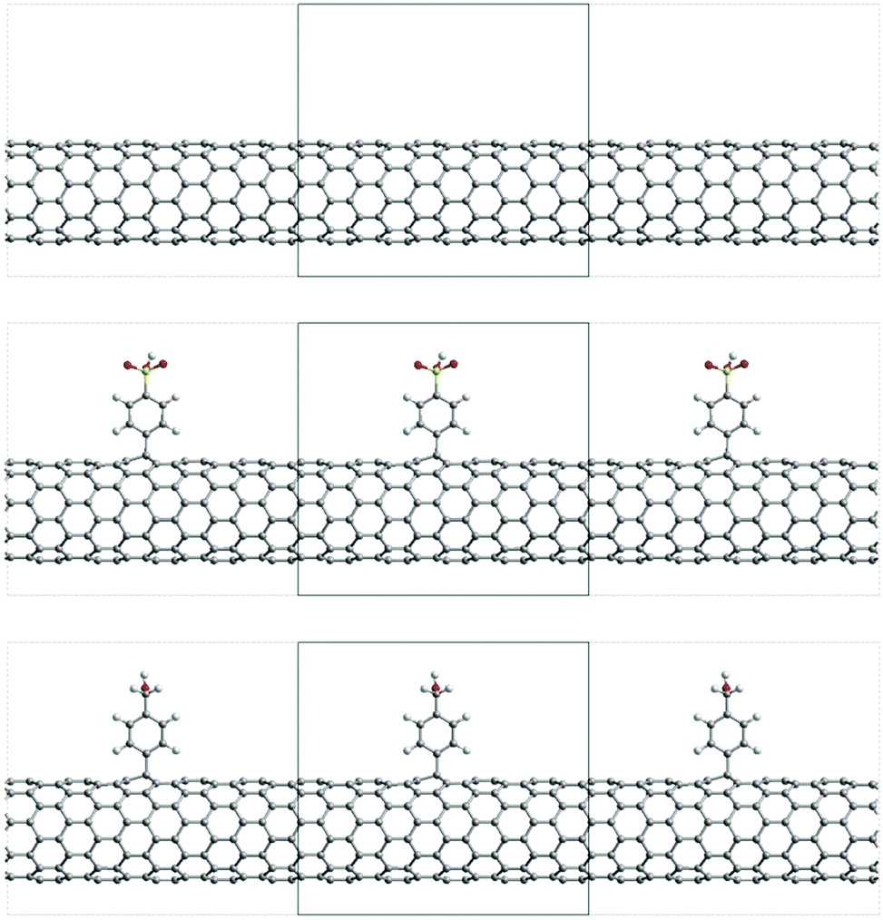 | ||
| Fig. 1 View of the unit cell of SWCNTs (top), A-SWCNTs (middle) and B-SWCNTs (bottom) for the (9,0) SWCNT family. | ||
Photoelectrochemistry
The photoelectrochemical experiments were performed using an AUTOLAB PGSTAT302N (Ecochemie) potentiostat. CV was carried out under a flow of nitrogen in a three-electrode cell using 0.1 M LiClO4 (Sigma Aldrich) in dry acetonitrile as the supporting electrolyte. Graphite and Ag/AgCl were used as the counter electrode and the reference electrode, respectively. The working electrode was prepared by spray coating 1 mL of SWCNT dispersions (0.02 mg mL−1) on commercial FTO substrates (Solems S.A., France) covering an area of ca. 1 cm2. Samples were illuminated through a quartz window using a 150 W Xe arc lamp (300 mW cm−2, LOT-Oriel 1.5 AM solar simulator, GmbH, Germany). On–off CV at a scan rate of 0.002 V s−1 was carried out by intermittently interrupting the passage of the light beam with a frequency of about 0.03 Hz.Results and discussion
Functionalization of SWCNTs
The functionalization degree on SWCNTs was first assessed by TGA (Fig. 2a). The organic moieties were quantified as follows: | (3) |
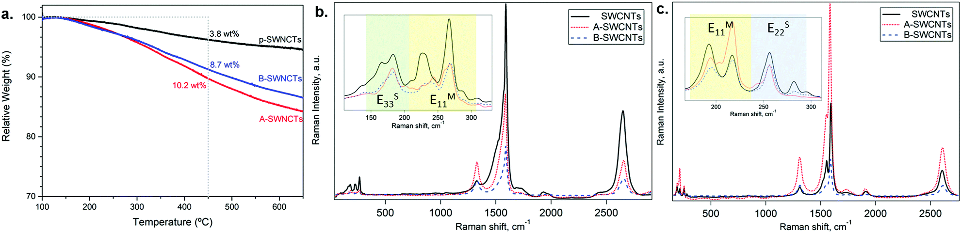 | ||
| Fig. 2 (a) TGA in an N2 atmosphere for SWCNTs (black lines), A-SWCNTs (red line) and B-SWCNTs (blue lines) in the range of 100–650 °C. Dotted lines delimit the range in which weight losses are considered for calculations. (b and c) Resonance Raman spectra and the RBM region (inset) of SWCNTs (black lines), A-SWCNTs (red dotted lines), and B-SWCNTs (blue dashed lines) excited by different laser lines: (b) 2.33 eV and (c) 1.96 eV. In the RBM region (inset), the green, yellow and blue regions correspond to the ES33, EM11 and ES22 electronic transitions, respectively. Each spectrum is an average based on 49 (2.33 eV) and 900 spectra (1.96 eV) measured at different points. | ||
In addition, we used another formula to estimate the functionalization degree in terms of the number of functional groups per X carbon atoms in SWCNTs (1/X):
 | (4) |
| A-SWCNTs | B-SWCNTs | |
|---|---|---|
| μmol g−1 | 407 | 457 |
| 1/X | 184 | 166 |
The functionalization reactions may strongly affect some of the SWCNTs’ optoelectronic properties, such as their UV/vis spectrum (Fig. S3 in the ESI†). In fact, the diazonium reactions of SWCNTs with 4-aminobenzenesulfonic acid and with benzyl alcohol derivatives, resulting in A-SWCNTs and B-SWCNTs, respectively, cause a total bleaching of the absorption bands of SWCNTs.
Raman spectroscopy
Raman spectroscopy under ambient conditions was performed for a preliminary assessment of the effects of covalent functionalization properties in A-SWCNTs and B-SWCNTs compared with SWCNTs (see Fig. 2b and c).The RBM, in which all carbon atoms of the SWCNT vibrate radially in phase, is observed at low Raman shifts between 100 and 350 cm−1. The energy of the RBM depends inversely on the SWCNT diameter.25 In Fig. 2b and c inset, changes in the RBM intensity and frequency are observed due to chemical functionalization. All the RBM bands of functionalized SWCNTs showed either bleaching or amplification compared with SWCNTs. However, nanotubes with mainly metallic character present large modifications in the RBM intensity (EM11 yellow region) upon functionalization, in good agreement with the previous literature.9,34
The tangential modes are the most intense in SWCNTs and form the G-band, which is related to in-plane C–C bond stretching, at around 1590 cm−1.25 The line shape of the G-band provides additional information about the metallic and semiconducting SWCNTs in resonance. With the 2.33 eV laser line, the G-band is highly asymmetric, which indicates that the band is narrower, indicating that mostly semiconducting SWCNTs are in resonance.45 The intensity and the position of the G-band change with functionalization (see Table 2). This could indicate changes in the electronic structure, in doping or in the resonance conditions of SWCNTs contributing to the G-band. This result suggested that the functional groups attached to the SWCNTs lead to a change in the doping level of SWCNTs.28 In addition, the SWCNT spectra presented in Fig. 2 reveal information about structural defects. The disorder-induced mode (the D-band) is observed at 1329 and 1312 cm−1 using 2.33 and 1.96 eV excitation energies, respectively.25 The D-band intensity depends on the laser energy and also correlates with the degree of functionalization.34,46 The D-band increases with functionalization due to the formation of sp3 defects on the nanotube surface where the functional group is covalently attached to the SWCNT wall (Table 2).
| 2.33 eV | 1.96 eV | |||
|---|---|---|---|---|
| G-Band shift (cm−1) | I D/IG | G-Band shift (cm−1) | I D/IG | |
| SWCNTs | 1593 | 0.07 | 1593 | 0.09 |
| A-SWCNTs | 1585 | 0.32 | 1585 | 0.20 |
| B-SWCNTs | 1590 | 0.29 | 1588 | 0.28 |
In situ Raman spectroelectrochemistry
In situ Raman spectroelectrochemistry was applied to investigate in detail the changes induced in the electronic structure of SWCNTs upon functionalization. Electrochemical charging can be understood using a double layer capacitor model, where the SWCNTs act as the working electrode and the charge carriers are injected into the SWCNTs, while the electrolyte ions compensate the charge. Extra electrons or holes from the circuit are inserted into the SWCNTs, causing changes in the electronic structure and these changes can be followed by Raman spectroscopy. Consequently, when the potential is changing, the charge transfer leads to a shift in the Fermi level. Taking into account the fact that the RBM intensity of SWCNTs is sensitive to the doping level,47,48 we have here specifically followed the changes upon functionalization with the electron-withdrawing and electron-donating molecules.The potential-dependent Raman spectra for the RBM region of the SWCNTs in the acetonitrile electrolyte solution are shown, as an example, in Fig. 3 (the spectra of A- and B-SWCNTs are shown in Fig. S4 and S5 in the ESI†). Sections (a) and (b) show the spectra obtained using 2.33 and 1.96 eV laser excitation energies, respectively. The positions of the most intense RBM bands are studied and the diameters of SWCNTs in resonance are estimated:49 183 (dt = 1.33 nm), 268 cm−1 (dt = 0.89 nm) in the case of laser energy Elaser = 2.33 eV, and 193 (dt = 1.24 nm) and 257 cm−1 (dt = 0.93 nm) at 1.96 eV laser excitation energy. When applying positive potentials, from 0 V to +1.5 V, in steps of 0.1 V, the Fermi level (EF) is downshifted (introducing holes into the π-band). The opposite occurs when negative potentials are applied, from 0 V to –1.5 V; the electron density increases due to the upshift in the EF value (introducing electrons into the π-band). In this way, when the EF value reaches a van Hove singularity (vHs), the corresponding electronic transition is blocked, and the Raman signal is bleached.
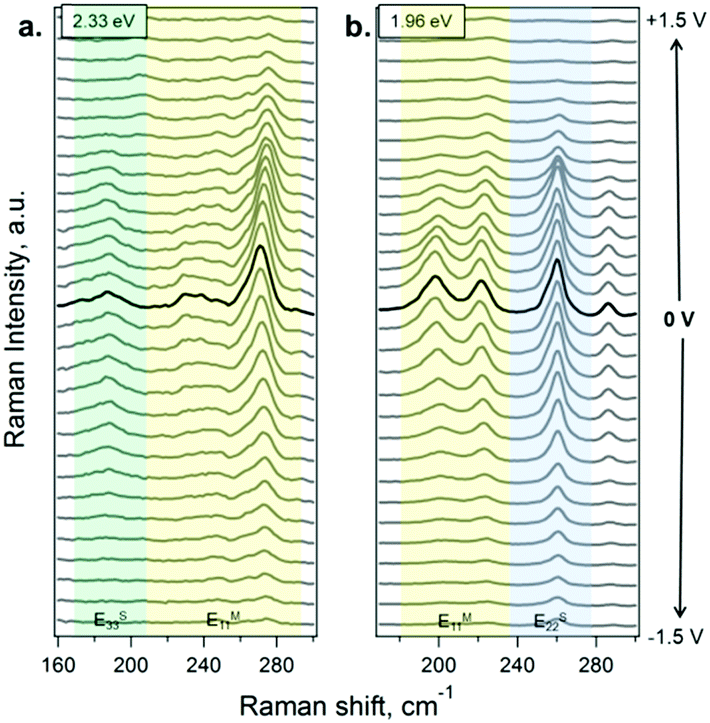 | ||
| Fig. 3 Raman spectra of the SWCNTs at different potentials in the RBM spectral region. The electrode potential range is from –1.5 to 1.5 V vs. the Ag pseudoreference electrode (from bottom to top). The spectra in bold correspond to the 0 V potential. The electrochemical potential change between the spectra is 0.1 V. The spectra were acquired using (a) 2.33 and (b) 1.96 eV laser excitation energies. The green, yellow and blue parts correspond to the regions where the used laser excitation energy matches ES33, EM11 and ES22 electronic transitions in the probed nanotubes, respectively. The spectra are offset for clarity. | ||
For a more detailed analysis of the SWCNT metallic/semiconducting character and the doping level, the dependence of the RBM intensity on the electrode potential at the selected laser lines was studied (see Fig. S6 in the ESI†). A difference in the profiles of the Raman intensity (IRBM) vs. applied potential (Eapp) of metallic and semiconducting SWCNTs has been previously reported.47,48 For semiconducting SWCNTs in resonance at 2.33 eV, the profile IRBMvs. Eapp exhibits a plateau close to 0 V. The IRBM profile is not significantly attenuated close to 0 V and starts changing only after the electrode potential reaches the first vHs. In contrast, the intensity of the band for metallic SWCNTs is attenuated at potentials close to 0 V. A similar effect occurs for the SWCNT in resonance at the laser excitation energy of 1.96 eV. Therefore, for semiconducting SWCNTs, the profile of IRBMvs. Eapp at around 0 V is a plateau and for the metallic SWCNT, it is sharp and shows a maximum. So one can distinguish between metallic and semiconducting SWCNTs.47 These assignments obtained using the IRBMvs. Eapp profiles are in agreement with the electronic transitions in the Kataura plot.49–51
The IRBMvs. Eapp profiles of the SWCNT, A- and B-SWCNT samples are shown in Fig. 4. The IRBM profiles of the bands in resonance via the EM11 transition reach a maximum at a given optimum potential. We found that maximum IRBM for the metallic SWCNT vs. Eapp is shifted for the functionalized samples in comparison with SWCNTs (Fig. 4b and c). In the case of semiconducting SWCNTs, there is no noticeable shift because of the occurrence of a plateau instead of a maximum. For both laser excitation energies, the profiles of IRBM in resonance via EM11 are downshifted for A-SWCNTs and upshifted for B-SWCNTs, in comparison to SWCNTs. This indicates that doping is induced on the SWCNTs by the functional groups attached to their walls. The benzenesulfonic acid moiety has a large electron affinity due to its structure composed of a benzene ring attached in the para position to a sulfur(VI) atom in a central part of a SO3H group. With three electronegative oxygen atoms, the SO3H group is strongly electron-withdrawing. It is necessary to apply an additional negative potential to reach the maximum peak of Raman intensity, pointing out that the A-SWCNTs are p-doped and the EF value is downshifted. In this way the valence band vHs is depleted and it is necessary to apply an extra negative potential to reach the neutral point. On the other hand, in the case of B-SWCNTs the maximum peak is shifted to positive potentials. This means that the EM11 transition becomes occupied (n-doped, filling) because EF is upshifted, as benzyl alcohol gives electrons to the SWCNT electronic structure.
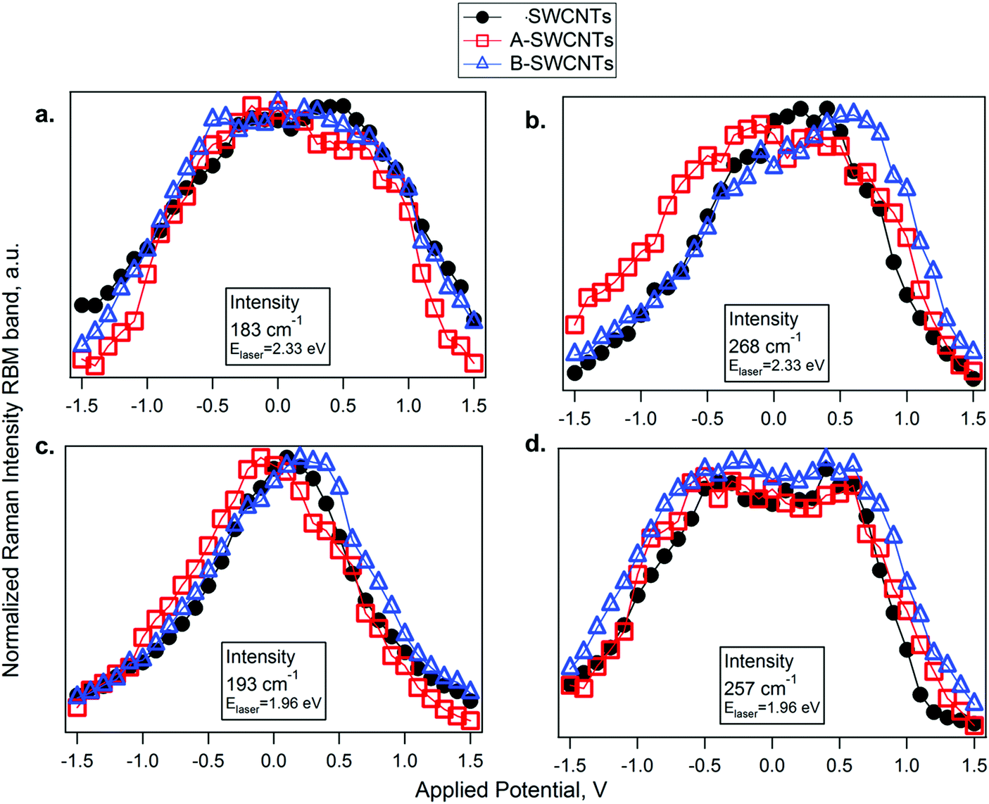 | ||
| Fig. 4 I RBM vs. E app for SWCNTs (black circles), A-SWCNTs (empty red squares) and B-SWCNTs (empty blue triangles) in resonance at 2.33 eV. (a and b) and 1.96 eV (c and d) for: (a) the band at 183 cm−1 (semiconducting ES33), (b) the band at 268 cm−1 (metallic EM11), (c) the band at 193 cm−1 (metallic EM11), and (d) the band at 257 cm−1 (semiconducting ES22). | ||
Theoretical calculations
DFT calculations have been carried out to support the Raman spectroelectrochemistry results. As an example, we study two SWCNT families in resonance with the laser lines at 2.33 and 1.96 eV (Fig. 5). The densities of states (DOS) of the functionalized SWCNTs have similar shapes but show shift in energy due to their different donor/acceptor substituents. | ||
| Fig. 5 DOS of the SWCNTs (dashed lines), A-SWCNTs (red lines) and B-SWCNTs (blue lines) for the two families studied. | ||
Theoretical calculations support that there is a shift in the Fermi level and the vHs due to the functionalization. As observed experimentally, the A-SWCNT functionalization yields a downward shift of the SWCNT Fermi level. On the other hand, the B-SWCNT functionalization takes place at the origin of an upward shift of the Fermi level with respect to the SWCNTs. The calculated shifts of the Fermi level are given in Table 3.
| E F (eV) | SWCNTs | A-SWCNTs | B-SWCNTs |
|---|---|---|---|
| (9,0) | −4.65 | −4.69 | −4.51 |
| (15,0) | −4.73 | −4.85 | −4.62 |
Photoelectrochemistry
The unique densities of states of SWCNTs allow the electron–hole separation upon photocurrent generation when they are exposed to light.52,53 Therefore, it can be expected that the doping effect induced in the functionalized SWCNTs would also be reflected in the photoelectrochemical properties. Testing the n-/p-doped functionalized SWCNT films in a three-electrode electrochemical cell, we study here the changes that occur in the photoresponse when chemical doping is introduced in the electronic structure of SWCNTs.Dark voltammograms for SWCNT, A-SWCNT and B-SWCNT film electrodes show the features that have been previously observed in the literature for similar systems, i.e. a ‘bow tie’ shape,54,55 with the narrowest part indicating the position of the Fermi level (see Fig. S7 in the ESI†).
Fig. 6 summarizes the changes observed by CV under illumination. In particular, the current in the cathodic branch of the scan is modified when the lamp is alternately switched on and off (Fig. 6a). Thus, the photocurrent can be calculated as the difference between consecutive on and off currents (Ilight − Idark) at various Eapp values (Fig. 6b). Photoanodic activity, typically less than 1 μA, was much lower than the photocathodic one (see Fig. S8, ESI†). When the three SWCNT electrodes are irradiated, a negative photocurrent appears at potentials lower than −0.4 V. In previous literature, photoelectroactivity for SWCNTs has been observed in another electrochemical reaction.56 In our work, the photocathodic process has to be observed at low scan rates (2 mV s−1), and the values observed for the photocurrent reached the noticeable value of ca. 20 μA. In these cases, the effects of the SWCNT functionalization are observed: A-SWCNTs show higher photocathodic currents than SWCNTs, indicating p-doping, while the contrary effect is observed for B-SWCNTs, indicating n-doping. Differences in photoanodic current between SWCNT, A-SWCNT and B-SWCNT films are not significant (see Fig. S9, ESI†). However, in the case of photocathodic current, the differences between SWCNT, A-SWCNT and B-SWCNT films are above 5 μA. These results are fully consistent with those described in the preceding sections, and indicate that the photoelectrochemical properties of SWCNTs can be tuned by chemical functionalization. Moreover, the chemically modified photoresponse can be predicted by using spectroelectrochemical techniques in a reliable manner, opening new possibilities in fields such as solar energy conversion and photosensors.
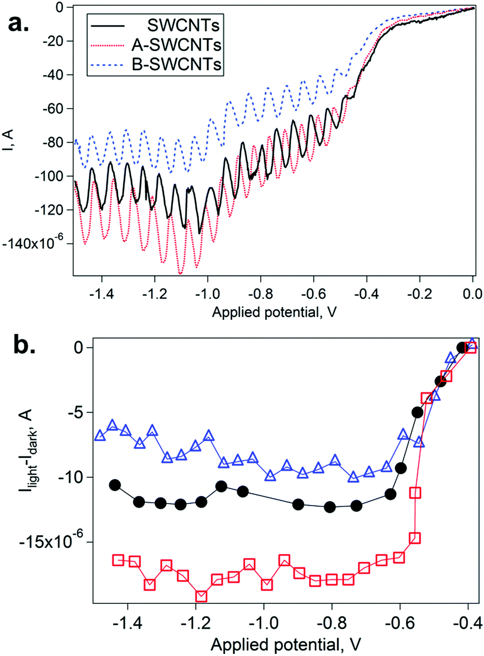 | ||
| Fig. 6 (a) Light–dark cathodic scans for SWCNT (black lines), A-SWCNT (red dotted lines) and B-SWCNT (blue dashed lines) films in 0.1 M LiClO4 acetonitrile. Scan rates of 2 mV s−1. (b) Photocurrent (Ilight − Idark) as a function of the Eapp value for SWCNT (black circles), A-SWCNT (empty red squares) and B-SWCNT (empty blue triangles) films. | ||
Conclusions
In summary, we have been able to determine the type of doping (n-/p-) of a bulk sample of chemically functionalized HiPco SWCNTs using an in situ Raman spectroelectrochemistry setup, studying the development of the RBM intensities in resonance via EM11 during electrochemical charging. This method, which is validated by DFT calculations, can constitute a routine test to estimate the electronic effects of SWCNT functionalization. It can also be used to predict the electronic properties of functionalized SWCNTs in devices. As a proof of principle, functionalized SWCNT films were used as electrodes in photoelectrochemistry measurements. The current under light irradiation was influenced by the functional group, in agreement with the spectroelectrochemical information and theoretical calculations. The procedure can be extended to other functional groups and/or other reactions in the chemistry of SWCNTs.Conflicts of interest
There are no conflicts to declare.Acknowledgements
The authors acknowledge financial support from the European Union FP7 RADDEL programme (ITN Marie Curie Actions PEOPLE-2011-290023) and the MEYS Inter Excellence Project no. LTC18039 and H2020-MSCA RISE Agreement no. 734834 (INFUSION). This work at the Instituto de Carboquímica has been funded by the MINECO and the European Regional Development Fund (ENE 2016-79282-C5-1-R), the Government of Aragon (T03-17R), and the European Commission (H2020-MSCA-ITN-2014-ETN 642742 ‘Enabling Excellence’). The work in Mons is supported by the European Union H2020 iSwitch programme (H2020-MSCA-ITN-2014-ETN 642196). Computational resources in Mons were provided by the Consortium des Équipements de Calcul Intensif (CÉCI) funded by the Belgian National Fund for Scientific Research (F.R.S.-FNRS) under Grant 2.5020.11. J. C. is an FNRS research director. The authors acknowledge the assistance provided by the Research Infrastructures NanoEnviCz (Project No. LM2015073) supported by the Ministry of Education, Youth and Sports of the Czech Republic and the project Pro-NanoEnviCz (Reg. no. CZ.02.1.01/0.0/0.0/16_013/0001821) supported by the Ministry of Education, Youth and Sports of the Czech Republic and the European Union – European Structural and Investments Funds in the frame of Operational Programme Research Development and Education. J. M. G.-D. is grateful to Spanish Ministry of Science, Innovation and Universities for his ‘Juan de la Cierva – Incorporación’ research grant. A. S. is grateful to Dr Sara Costa and Dr Johan Ek Weis for fruitful discussions and helpful comments.Notes and references
- V. Georgakilas, J. A. Perman, J. Tucek and R. Zboril, Chem. Rev., 2015, 115, 4744–4822 CrossRef CAS PubMed.
- M. F. L. De Volder, S. H. Tawfick, R. H. Baughman and A. J. Hart, Science, 2013, 339, 535–539 CrossRef CAS PubMed.
- K. Chen, W. Gao, S. Emaminejad, D. Kiriya, H. Ota, H. Y. Yin Nyein, K. Takei and A. Javey, Adv. Mater., 2016, 28, 4397–4414 CrossRef CAS PubMed.
- L. Yu, C. Shearer and J. Shapter, Chem. Rev., 2016, 116, 13413–13453 CrossRef CAS PubMed.
- P. Prakash, K. Mohana Sundaram and M. Anto Bennet, Renewable Sustainable Energy Rev., 2018, 89, 194–203 CrossRef CAS.
- S. A. Hodge, M. K. Bayazit, K. S. Coleman and M. S. P. Shaffer, Chem. Soc. Rev., 2012, 41, 4409–4429 RSC.
- S. Mallakpour and S. Soltanian, RSC Adv., 2016, 6, 109916 RSC.
- A. Setaro, J. Phys.: Condens. Matter, 2017, 29, 423003 CrossRef CAS PubMed.
- M. S. Strano, C. A. Dyke, M. L. Usrey, P. W. Barone, M. J. Allen, H. Shan, C. Kittrell, R. H. Hauge, J. M. Tour and R. E. Smalley, Science, 2003, 301, 1519–1522 CrossRef CAS PubMed.
- V. Sgobba and D. M. Guldi, Chem. Soc. Rev., 2009, 38, 165–184 RSC.
- K. Dirian, M. A. Herranz, G. Katsukis, J. Malig, L. Rodriguez-Perez, C. Romero-Nieto, V. Strauss, N. Martin and D. M. Guldi, Chem. Sci., 2013, 4, 4335–4353 RSC.
- M. Scardamaglia, C. Struzzi, F. J. Aparicio Rebollo, P. De Marco, P. R. Mudimela, J.-F. Colomer, M. Amati, L. Gregoratti, L. Petaccia, R. Snyders and C. Bittencourt, Carbon, 2015, 83, 118–127 CrossRef CAS.
- J. L. Bahr and J. M. Tour, Chem. Mater., 2001, 13, 3823–3824 CrossRef CAS.
- G. Schmidt, S. Gallon, S. Esnouf, J.-P. Bourgoin and P. Chenevier, Chem. – Eur. J., 2009, 15, 2101–2110 CrossRef CAS PubMed.
- B. Dinesh, A. Bianco and C. Menard-Moyon, Nanoscale, 2016, 8, 18596–18611 RSC.
- Y. Piao, B. Meany, L. R. Powell, N. Valley, H. Kwon, G. C. Schatz and Y. Wang, Nat. Chem., 2013, 5, 840 CrossRef CAS PubMed.
- M. Kim, L. Adamska, N. F. Hartmann, H. Kwon, J. Liu, K. A. Velizhanin, Y. Piao, L. R. Powell, B. Meany, S. K. Doorn, S. Tretiak and Y. Wang, J. Phys. Chem. C, 2016, 120, 11268–11276 CrossRef CAS.
- L. R. Powell, Y. Piao and Y. Wang, J. Phys. Chem. Lett., 2016, 7, 3690–3694 CrossRef CAS PubMed.
- A. López-Bezanilla, F. Triozon, S. Latil, X. Blase and S. Roche, Nano Lett., 2009, 9, 940–944 CrossRef PubMed.
- F. Teichert, A. Zienert, J. Schuster and M. Schreiber, Comput. Mater. Sci., 2017, 138, 49–57 CrossRef CAS.
- J. L. Blackburn, A. J. Ferguson, C. Cho and J. C. Grunlan, Adv. Mater., 2018, 30, 1704386 CrossRef PubMed.
- T. Ketolainen, V. Havu, E. Ö. Jónsson and M. J. Puska, Phys. Rev. Appl., 2018, 9, 034010 CrossRef.
- C. Romero-Nieto, R. García, M. Á. Herranz, L. Rodríguez-Pérez, M. Sánchez-Navarro, J. Rojo, N. Martín and D. M. Guldi, Angew. Chem., Int. Ed., 2013, 52, 10216–10220 CrossRef CAS PubMed.
- N. V. Kurnosov, V. S. Leontiev, A. S. Linnik and V. A. Karachevtsev, Chem. Phys. Lett., 2015, 623, 51–54 CrossRef CAS.
- M. S. Jorio, R. Saito and G. Dresselhaus, Raman Spectroscopy in Graphene Related Systems, J. W. Sons, 2011 Search PubMed.
- B. Nikolić, I. Milošević and M. Damnjanović, J. Phys. Chem. C, 2014, 118, 20576–20584 CrossRef.
- H.-J. Shin, S. M. Kim, S.-M. Yoon, A. Benayad, K. K. Kim, S. J. Kim, H. K. Park, J.-Y. Choi and Y. H. Lee, J. Am. Chem. Soc., 2008, 130, 2062–2066 CrossRef CAS PubMed.
- R. Voggu, C. S. Rout, A. D. Franklin, T. S. Fisher and C. N. R. Rao, J. Phys. Chem. C, 2008, 112, 13053–13056 CrossRef CAS.
- C. N. R. Rao and R. Voggu, Mater. Today, 2010, 13, 34–40 CrossRef CAS.
- K. Ladislav and D. Lothar, ChemPhysChem, 2007, 8, 974–998 CrossRef PubMed.
- D. Ibañez, J. Garoz-Ruiz, D. Plana, A. Heras, D. J. Fermín and A. Colina, Electrochim. Acta, 2016, 217, 262–268 CrossRef.
- M. Kierkowicz, E. Pach, A. Santidrián, E. Tobías-Rossell, M. Kalbáč, B. Ballesteros and G. Tobias, ChemNanoMat, 2016, 2, 108–116 CrossRef CAS.
- Y. Zhai, Z. Zhu, S. Zhou, C. Zhu and S. Dong, Nanoscale, 2018, 10, 3089–3111 RSC.
- J. M. González-Domínguez, A. Santidrián, A. Criado, C. Hadad, M. Kalbáč and T. D. Ros, Chem. – Eur. J., 2015, 21, 18631–18641 CrossRef PubMed.
- V. V. Pavlishchuk and A. W. Addison, Inorg. Chim. Acta, 2000, 298, 97–102 CrossRef CAS.
- W. Kohn, Rev. Mod. Phys., 1999, 71, 1253–1266 CrossRef CAS.
- D. Sánchez-Portal, P. Ordejón, E. Artacho and J. M. Soler, Int. J. Quantum Chem., 1997, 65, 453–461 CrossRef.
- J. P. Perdew, K. Burke and M. Ernzerhof, Phys. Rev. Lett., 1996, 77, 3865–3868 CrossRef CAS PubMed.
- J. M. Soler, E. Artacho, J. D. Gale, A. García, J. Junquera, P. Ordejón and D. Sánchez-Portal, J. Phys.: Condens. Matter, 2002, 14, 2745 CrossRef CAS.
- N. Troullier and J. Martins, Solid State Commun., 1990, 74, 613–616 CrossRef.
- R. Dovesi, R. Orlando, B. Civalleri, C. Roetti, R. Saunders Victor and M. Zicovich-Wilson Claudio, Z. Kristallogr. – Cryst. Mater., 2005, 220, 571 CAS.
- C. Adamo and V. Barone, J. Chem. Phys., 1999, 110, 6158–6170 CrossRef CAS.
- H. C. Bai and L. You, Int. J. Sci., 2014, 1, 48–52 Search PubMed.
- L.-C. Yin, H.-M. Cheng, R. Saito and M. S. Dresselhaus, Carbon, 2011, 49, 4774–4780 CrossRef CAS.
- M. A. Pimenta, A. Marucci, S. A. Empedocles, M. G. Bawendi, E. B. Hanlon, A. M. Rao, P. C. Eklund, R. E. Smalley, G. Dresselhaus and M. S. Dresselhaus, Phys. Rev. B: Condens. Matter Mater. Phys., 1998, 58, R16016 CrossRef CAS.
- J. Maultzsch, S. Reich and C. Thomsen, Phys. Rev. B: Condens. Matter Mater. Phys., 2001, 64, 121407 CrossRef.
- M. Kalbac, H. Farhat, L. Kavan, J. Kong, K.-i. Sasaki, R. Saito and M. S. Dresselhaus, ACS Nano, 2009, 3, 2320–2328 CrossRef CAS PubMed.
- F. Dragin, A. Pénicaud, M. Iurlo, M. Marcaccio, F. Paolucci, E. Anglaret and R. Martel, ACS Nano, 2011, 5, 9892–9897 CrossRef CAS PubMed.
- P. T. Araujo, P. B. C. Pesce, M. S. Dresselhaus, K. Sato, R. Saito and A. Jorio, Phys. E, 2010, 42, 1251–1261 CrossRef CAS.
- H. Kataura, Y. Kumazawa, Y. Maniwa, I. Umezu, S. Suzuki, Y. Ohtsuka and Y. Achiba, Synth. Met., 1999, 103, 2555–2558 CrossRef CAS.
- D. Zhang, J. Yang, F. Yang, R. Li, M. Li, D. Ji and Y. Li, Nanoscale, 2015, 7, 10719–10727 RSC.
- S. Barazzouk, S. Hotchandani, K. Vinodgopal and P. V. Kamat, J. Phys. Chem. B, 2004, 108, 17015–17018 CrossRef CAS.
- M. Engel, M. Steiner, R. S. Sundaram, R. Krupke, A. A. Green, M. C. Hersam and P. Avouris, ACS Nano, 2012, 6, 7303–7310 CrossRef CAS PubMed.
- S. A. Hodge, M. K. Bayazit, H. H. Tay and M. S. P. Shaffer, Nat. Commun., 2013, 4, 1989 CrossRef PubMed.
- S. A. Hodge, S. Fogden, C. A. Howard, N. T. Skipper and M. S. P. Shaffer, ACS Nano, 2013, 7, 1769–1778 CrossRef CAS PubMed.
- M. A. Bissett and J. G. Shapter, J. Electrochem. Soc., 2011, 158, K53–K57 CrossRef CAS.
Footnote |
| † Electronic supplementary information (ESI) available: Further details of the purification of SWCNTs, reagents and solvents used; deconvolution of the D-band and the G-band; DOS of the SWCNTs for the structure optimized with SIESTA and CRYSTAL; UV-vis absorbance spectra of SWCNTs, A-SWCNTs and B-SWCNTs; the RBM region of Raman spectra at different Eapp values for A-SWCNTs and B-SWCNTs; dark voltammograms for SWCNTs, A-SWCNTs and B-SWCNTs. See DOI: 10.1039/c8cp06961a |
| This journal is © the Owner Societies 2019 |