
 Open Access Article
 This Open Access Article is licensed under a Creative Commons Attribution-Non Commercial 3.0 Unported Licence
Single crystal growth of bulk InGaZnO4 and analysis of its intrinsic transport properties†
Yusuke
Tanaka
a,
Kazuhiro
Wada
a,
Yuki
Kobayashi
a,
Takenori
Fujii
 b,
Saleem J.
Denholme
a,
Ryotaro
Sekine‡
a,
Naoki
Kase
a,
Noboru
Kimizuka
c and
Nobuaki
Miyakawa
*a
b,
Saleem J.
Denholme
a,
Ryotaro
Sekine‡
a,
Naoki
Kase
a,
Noboru
Kimizuka
c and
Nobuaki
Miyakawa
*a
aDepartment of Applied Physics, Tokyo University of Science, 6-3-1 Niijuku, Katsushika-ku, Tokyo 125-8585, Japan. E-mail: miyakawa@rs.tus.ac.jp
bCryogenic Research Center, University of Tokyo, 2-11-16 Yayoi, Bunkyo, Tokyo 113-0032, Japan
cDepartamento de Investigación en Polímeros y Materiales, Universidad de Sonora, Rosales y Luis Encinas s/n, Hermosillo, Sonora CP 83000, Mexico
First published on 4th April 2019
Abstract
The establishment of a reliable method for the growth of bulk In–Ga–Zn–O single crystals is important not only to investigate the fundamental and peculiar properties specific to this material but also for its development for novel functional devices. Large bulk single crystals of InGaZnO4 have been successfully grown using an optical floating zone method under a flow of dry-air at high-pressure. The stoichiometric InGaZnO4 single crystals were obtained at a gas pressure of 0.9 MPa using a feed rod with a Zn-rich composition, where the lattice constants are a = 3.2990(4) Å and c = 26.018(3) Å as the hexagonal expression for the rhombic system (space group R![[3 with combining macron]](https://www.rsc.org/images/entities/char_0033_0304.gif) m, No. 166). The as-grown single crystals exhibit a blueish colour, but become transparent after annealing in oxygen. Upon post-annealing, the carrier density, the conductivity in the ab-plane and the mobility at room temperature changes in the range from ∼1020 to ∼1017 cm−3, from ∼2000 to ∼1 S cm−1, and from ∼100 to ∼10 cm2/(Vs), respectively. In addition, we found that the conductivity along the c-axis is much lower than that of the ab-plane in InGaZnO4 single crystals, and that the anisotropy increases with decreasing carrier density.
m, No. 166). The as-grown single crystals exhibit a blueish colour, but become transparent after annealing in oxygen. Upon post-annealing, the carrier density, the conductivity in the ab-plane and the mobility at room temperature changes in the range from ∼1020 to ∼1017 cm−3, from ∼2000 to ∼1 S cm−1, and from ∼100 to ∼10 cm2/(Vs), respectively. In addition, we found that the conductivity along the c-axis is much lower than that of the ab-plane in InGaZnO4 single crystals, and that the anisotropy increases with decreasing carrier density.
1. Introduction
Transparent conducting oxides (TCOs) have received considerable attention as materials for transparent electrodes, high-performance thin film transistors (TFTs) for liquid displays and organic light-emitting diodes. In general, electrical conductivity and transparency are incompatible and therefore TCOs stand out for their ability to exhibit both characteristics. A prime example of TCOs is multicomponent oxides, which can exhibit a variety of crystal structures and a range of functional properties suitable for device applications. In addition, ionic oxides containing post-transition metal cations with the electronic configuration (n − 1)d10ns0 can become TCOs.1 One such example is the In–Ga–Zn-oxides, where the electronic configurations of In3+, Ga3+ and Zn2+ are 4d105s0, 3d104s0 and 3d104s0, respectively. These are a family of compounds with the general formula (InGaO3)m(ZnO)n (m, n = natural number; hereafter referred to as IGZO-mn), and were originally synthesized by Kimizuka et al.2,3A multicomponent oxide with a layered structure is expected not only to exhibit anisotropic conduction properties but also to show other interesting phenomena4–8 such as high temperature superconductivity in multicomponent oxides containing Cu. Here, a series of IGZO-mn is a multicomponent oxide with a layered structure. Therefore, materials like IGZO-mn have attracted significant attention.
In particular, IGZO-1n thin films, which include amorphous-IGZO (a-IGZO)9 and c-axis-aligned crystal IGZO (CAAC-IGZO),10,11 are promising channel materials for TFTs, due to their high-mobility9,12 and high optical transparency.9,13,14 Furthermore IGZO-1n-based TFTs exhibit not only a higher on-state current but also an extremely lower off-state current.13,15,16 Therefore, the IGZO-mn TFTs are already a common component in liquid crystal displays.17 In optoelectronic devices for industrial applications, materials having high electrical conductivity and a large energy gap are useful. In this view, polycrystalline IGZO-11 (i.e. InGaZnO4) exhibits the highest conductivity and the largest optical band gap among the IGZO-1n family.18 Therefore, due to its optoelectronic properties, IGZO-11 will be the most attractive material for industrial applications. However, single crystals of bulk IGZO-11 with a sufficient size to measure their physical properties have not yet been achieved and so the precise intrinsic properties of IGZO-11 crystals remain unknown. The motivation of the present manuscript is to establish a reliable method for the growth of large, high-quality bulk IGZO-11 single crystals and to determine its electrical and optical properties.
However, the growth of IGZO-11 single crystals is difficult for three main reasons: 1) IGZO-11 exhibits a multicomponent layered structure, which easily leads to defect formation during single crystal growth. 2) One of the required reactants ZnO has a high-vapour pressure, and evaporates easily at the high-temperatures required. 3) It is unclear if IGZO-11 is a congruently or incongruently melting material. Even the melting point has not yet been determined and therefore determining the required synthesis parameters is challenging.
Currently, the growth of IGZO-11 single crystal has been done using solid state reaction methods.19,20 However, these methods also produce a high quantity of defects, and the cation ratio is reported to be In![[thin space (1/6-em)]](https://www.rsc.org/images/entities/char_2009.gif) :Ga:Zn = 30:39:31.20 In addition, the size of the crystals is considerably small, of the order of a few hundred micrometres.20 The growth of single crystalline thin films of IGZO-1n using the so-called reactive solid-phase epitaxy (R-SPE) method has been achieved by Ohta et al.21 This is due to the fact that IGZO-11 does not exhibit a liquid phase at temperatures lower than 1550 °C, that is, liquid-phase epitaxy and vapour–liquid–solid methods cannot be used to grow IGZO-11 thin films. The R-SPE method was developed from a method originally reported by Isobe et al.,22 who achieved the growth of small single crystalline grains of LuFeO3(ZnO) which is a isostructural material with IGZO-11. However, high-quality bulk single crystals have not been realized yet. Thus, it is necessary to develop a new and different crystal growth method to obtain high-quality macro-sized IGZO-11 single crystals, which will allow for the analysis of its intrinsic properties.
:Ga:Zn = 30:39:31.20 In addition, the size of the crystals is considerably small, of the order of a few hundred micrometres.20 The growth of single crystalline thin films of IGZO-1n using the so-called reactive solid-phase epitaxy (R-SPE) method has been achieved by Ohta et al.21 This is due to the fact that IGZO-11 does not exhibit a liquid phase at temperatures lower than 1550 °C, that is, liquid-phase epitaxy and vapour–liquid–solid methods cannot be used to grow IGZO-11 thin films. The R-SPE method was developed from a method originally reported by Isobe et al.,22 who achieved the growth of small single crystalline grains of LuFeO3(ZnO) which is a isostructural material with IGZO-11. However, high-quality bulk single crystals have not been realized yet. Thus, it is necessary to develop a new and different crystal growth method to obtain high-quality macro-sized IGZO-11 single crystals, which will allow for the analysis of its intrinsic properties.
The use of methods such as the Czochralski- and Bridgman-techniques, which are based on the supercooling of the liquid phase, can be applied only to congruently melting materials. On the other hand, an optical floating zone (OFZ) method23 can be applied to both congruently24 and incongruently4,25 melting compounds if a stable liquid-phase can be achieved. Therefore for IGZO-11 which may be an incongruently melting material, the application of a solution growth method such as the OFZ method is instead a potential solution. In this case, the driving force of the crystallization is supersaturation, which originates from the slow cooling of the solution and evaporation of the solvent. The OFZ method is particularly advantageous to grow large, high-quality single crystals, and it is due to the liquid-phase method that no crucible is necessary.
Up to now, the transport properties of the IGZO-1n family have been extensively studied. Most studies have been conducted on polycrystalline samples,12,18,26 single crystal thin films13,27 and amorphous thin films.28–30 In addition, TFT characteristics using a-IGZO and/or CAAC-IGZO films have been investigated.9,10,13,17,31–37 In contrast, there have been few detailed investigations of the physical properties of bulk IGZO-mn single crystals such as IGZO-11. If a reliable synthesis method can be established, the intrinsic-properties of IGZO-mn single crystal such as its electronic structure, bulk conductivity, mobility and thermal properties can finally be clarified. In general, thin film transport data may differ from those of bulk single crystals, since lattice mismatch between the film and the substrate can affect the measured properties.38 Furthermore, for polycrystalline samples it is impossible to investigate the anisotropic properties of the electrical conductivity etc. Consequently, the intrinsic carrier-generation mechanisms of IGZO-11 have not yet been fully clarified. In addition, the material is prone to develop defects during crystal growth such as (i) cation-defects, (ii) oxygen-vacancies and (iii) substitution among cations (antisite). As a result it is difficult to determine the fundamental properties which derive the original crystal structure of IGZO-11 rather than those that are the consequence of structural defects.
In this paper, we report a novel and reproducible method for the growth of the large and high-quality IGZO-11 single crystals. Our method incorporates the use of OFZ under high-pressure using a feed rod with a Zn-rich composition. We visually confirm the presence of a stable liquid phase at a pressure of ∼0.9 MPa. In addition, it is found that IGZO-11 is an incongruently-melting compound and melts at about 1650 °C. By obtaining large, high-quality single crystals we are able to determine the intrinsic transport properties such as the anisotropic electrical conductivity. We find that the ratio between the in-plane and out-of-plane conductivity strongly depends on carrier density. In addition, post annealing in oxygen was applied to elucidate the relationship between oxygen vacancy and the physical characteristics of IGZO-11.
2. Experimental details
2.1. Single crystal preparation
IGZO-11 single crystals were prepared using an infrared image furnace equipped with double ellipsoidal mirrors (NEC-SCII-EDH) where 1.5 kW halogen lamps were used as a heat source. The synthesis details are as follows:The feed rods were prepared by a standard solid-phase reaction method using high purity reactants. Firstly, In2O3, Ga2O3 and ZnO powders (purity 99.99%) were preheated at 1250 °C in air for 24 h. Using a molar ratio of 1:1:2 + x (0 ≤ x ≤ 0.2) of In2O3:Ga2O3:ZnO, the powders were mixed in ethanol using an agate mortar for 30 min. After drying, the mixture was ground further for another 2 h and (i) calcined at 1250 °C for 2 days. (ii) The calcined powder was then reground for 1–2 h. Processes (i) and (ii) were repeated twice more. The prepared mixture was tightly packed into a rubber tube with 6 mm in diameter, which was then evacuated using a rotary pump for 30 min in order to increase both its density and uniformity. The tube was then hydrostatically pressed at a pressure of 18 MPa for 15 min to form a rod-like shape. The rod was sintered at 1250 °C for 24 h in air. A sintered rod with a ∼5 mm diameter was typically 100–150 mm in length.
The sintered rod can also be used as the support rod (prior to the formation of the first batch of single crystals, which are later used as the seed). The feed and support (or seed) rods were set into an infrared radiation furnace. Single crystals of In–Ga–Zn–O have been grown at a growth rate of 1.9 mm h−1, gap speed of 2.0 mm h−1 under a constant gas flow of dry-air with a pressure in the quartz tube in the range of 0.1–0.9 MPa. The upper and the lower shafts were counter-rotated at a rate of 16 and 14 rpm, respectively, to minimize the diffusion layer close to the crystallization front by thorough mixing of the solvent zone.
In order to investigate the effect of oxygen defects, cleaved single crystals with a thickness of approx. 0.2 mm and a length of around 1–5 mm are annealed under a flow of O2 at 800–1250 °C for between 10 h–2 weeks.
2.2. Characterization of single crystals
Powder X-ray diffraction (PXRD) was performed in the range of 4° ≤ 2θ ≤ 90° with a RINT2500V diffractometer (Rigaku, Japan) using flat plate geometry with Cu-Kα radiation (λ = 1.5418 Å). Lattice constants were calculated using the least-squares method for patterns with 15 reflections or more, where Si powder was used as the standard specimen to determine the d-spacing. In order to determine the composition ratio for the as-grown crystals, X-ray fluorescence (XRF) analysis was performed on bulk single crystals (size: 2–4 mm) using a JSX-1000S spectrometer (JEOL, Japan) with a 0.9 mm diameter spot.The optical transmittance spectra of the IGZO-11 single crystals (thickness 0.195 mm) were measured before and after annealing with a U-3010 spectrophotometer (Hitachi High-Tech Science Corporation, Japan). By assuming that the reflectance R can be ignored, the absorption coefficient α was calculated by α = −ln{T/(1 − R)2}/d ≈ −ln(T)/d, where T is the transmittance and d is the thickness of a single crystal. The optical band gap Eg of the bulk single crystals is evaluated using the Tauc method.39,40 It is known that the absorption coefficient α is related to the incident photon energy hν by the following formula,
| αhν = β(hv − Eg)N |
The dc in-plane electrical conductivity σab was measured by a four-probe method at a temperature range of 4–300 K, where Ag (or Au) paste was used for the electrical contacts. Out-of-plane conductivity σc was also measured with a four-probe-like method, where in the case of the thinner single crystals the voltage contacts were attached to the centre of the flat surface (ab-plane) and the current contacts were attached to cover most of the remaining space of the sample. Alternatively in the case of thicker crystals (thickness > 1 mm) the voltage contacts were attached to the side of crystal, which is perpendicular to ab-pane and the current contacts were attached to cover the ab-plane of single crystal by Ag (or Au) paste. The Hall resistivity was measured by a 6-wire method using a physical properties measurement system (Quantum Design Co., Ltd), where a magnetic field of ±5 T was applied perpendicular to the current flow (ab-plane). The carrier density ne and Hall mobility μe were estimated from the Hall coefficient RH using the relation ne = 1/qRH and μe = σabRH, where q is an elementary charge.
3. Results and discussion
3.1. Optimal conditions for the growth of bulk IGZO-11 single crystals, and their characterization
IGZO-11 crystals were first grown using the OFZ method under atmospheric pressure. During the synthesis, the vaporization of a substance from the molten zone was observed (although the IGZO-11 rod completely melted at temperatures above 1650 °C). The vaporized substance deposited on the quartz-tube walls which line the infrared radiation furnace. The substance evaporated and deposited is identified as mainly crystalline ZnO using PXRD analysis. However, it appears that some oxides consisting of both In and Zn are also present, and here they are presumed to be In–Zn–O-based compounds such as In2O3(ZnO)17 (see Fig. S1†). In addition, the Bragg reflection peaks are quite broad (but not amorphous), and this is typical for XRD patterns where a substance exhibits small particle size and/or insufficient crystallinity. Furthermore, the main phase of the as-grown crystals was the IGZO-21 (i.e. In2Ga2ZnO7) (see Fig. S2†). This suggests that the IGZO-21 is precipitated as the primary phase from the molten zone as the ZnO vaporises. This can be summarized in the following chemical reaction, 2InGaO3(ZnO)rod → (InGaO3)2ZnO + ZnO↑. This result suggests that IGZO-11 is an incongruently melting compound. As seen in Fig. S2,† the IGZO-11 phase was also observed together along with the dominant IGZO-21 phase, implying that the growth of IGZO-11 single crystals is achievable.From these results we can conclude that it is necessary to prevent the vaporization of ZnO, in order to achieve a stable liquid phase in the molten zone and to precipitate IGZO-11 as the primary product. With this in mind we adopted the following two methods: (i) conduct the synthesis under a flow of dry-air to create a pressurized atmosphere of P = 0.1–0.9 MPa, and (ii) use a feed rod with a Zn-rich composition to provide a continuous supply of ZnO during crystal growth.
In order to find the optimal growth conditions, the synthesis was performed under pressures of 0.1, 0.6 and 0.9 MPa for feed rods with a stoichiometric ratio (In:Ga:Zn = 1:1:1) or pressures of 0.8 and 0.9 MPa for feed rods with a Zn-rich starting mixture (In:Ga:Zn = 1:1:1.1) respectively. The presence of IGZO-21 was checked by PXRD post synthesis. We found that the XRD peak-intensity of IGZO-21 decreases with increasing gas pressure and/or using a feed rod with a Zn-rich composition (see Fig. S3†). This demonstrates that pressures ≤0.9 MPa are able to effectively reduce the vaporization of ZnO, but cannot suppress it completely. The ratio of the reactants, gas pressures, obtained phases and lattice constants of the IGZO-11 (=1114) phase are summarized in Table 1, where the phases 1114 and 2217 represent InGaZnO4 (=IGZO-11) and In2Ga2ZnO7 (=IGZO-21), respectively.
| Growth condition name | In2O3:Ga2O3:ZnO (molar ratio) |
Gas pressure (MPa) | Phase | a (Å) | c (Å) |
|---|---|---|---|---|---|
| #P01Z10 | 1.0:1.0:2.0 |
0.1 | 1114 + 2217 | 3.293(4) | 26.03(3) |
| #P06Z10 | 1.0:1.0:2.0 |
0.6 | 1114 + 2217 | 3.292(2) | 26.02(2) |
| #P08Z11 | 1.0:1.0:2.2 |
0.8 | 1114 + 2217 | 3.2985(3) | 26.016(3) |
| #P09Z10 | 1.0:1.0:2.0 |
0.9 | 1114 + 2217 | 3.2995(3) | 26.021(3) |
| #P09Z11 | 1.0:1.0:2.2 |
0.9 | 1114 | 3.2990(4) | 26.018(3) |
| Polycrystalline | 1.0:1.0:2.0 |
— | 1114 | 3.2986(3) | 26.019(3) |
Under the growth conditions (#P09Z11) outlined in Table 1, high-quality IGZO-11 single crystals on the cm-scale were successfully grown as shown in Fig. 1(a) and (b). During the crystal growth we were able to observe the stable molten zone at the interface between the liquid and a solid using a CCD camera.
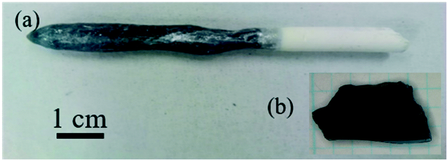 | ||
| Fig. 1 (a) The rod-shaped InGaZnO4 crystal grown by the OFZ method under a pressure of 0.9 MPa and (b) the plate-shaped single crystal which was cleaved mechanically from the rod-shaped crystal, where the cleavage plane is perpendicular to the c-axis. The thickness of the plate-shaped crystal is approximately 0.66 mm. | ||
Fig. 1(a) shows an image of an as-grown IGZO-11 crystal bar, where growth primarily occurs along the ab-plane. The obtained crystals exhibit a blueish colour although the strength of the colour depth depends on the thickness of the crystal, and the crystals can be easily cleaved. Fig. 1(b) shows a layer cleaved mechanically from the bar. It has a plate-like shape, where the clean and flat surface is perpendicular to the c-axis. This anisotropic crystal-growth is related to the difference in surface energy at each crystal plane since the growth rate of the crystal plane with the higher surface energy increases.
Fig. 2(a) shows the XRD pattern for an as-grown single crystal (#P09Z11). All the peaks can be assigned to the (00l) reflections of IGZO-11 suggesting that the cleaved surface is perpendicular to the c-axis. This result is consistent with that calculated by Yamazaki et al.10 who reported that the smallest cleavage energy was between two (Ga,Zn)O planes. Fig. 2(b) shows the PXRD pattern for (#P09Z11), where only the IGZO-11 phase is observed, which confirms the absence of impurity phases. IGZO-11 crystallizes with the rhombic system (space group Rm, No. 166) and the calculated lattice constants are a = 3.2990(4) Å, c = 26.018(3) Å as the hexagonal expression which are almost consistent with those for stoichiometric polycrystalline IGZO-11, where a = 3.2948(1) Å, c = 26.071(1) Å.2 It is known that the a-axis lattice constant of the IGZO-11 phase becomes smaller with increasing Zn vacancies.20 From Table 1, we can confirm that the a-axis lattice constants of samples grown at the lower pressures of 0.1 and 0.6 MPa (#P01Z10 and #P06Z10) are smaller than those of the stoichiometric polycrystalline IGZO-11 (e.g. 1114) whose PXRD pattern is shown in Fig. 2(c). On the other hand, the lattice constants of samples grown at higher pressures of 0.8 and 0.9 MPa (#P08Z11, #P09Z10 and #P09Z11) are equivalent to the values of the polycrystalline samples. This coincidence in the lattice parameters suggests that crystals grown using the conditions for (#P08Z11, #P09Z10 and #P09Z11) possess only a small reduction in the amount of Zn vacancies in the IGZO-11 phase, compared to those for #P01Z10 and #P06Z10.
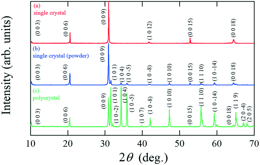 | ||
| Fig. 2 XRD patterns of IGZO-11 using Cu-Kα radiation (λ = 1.5418 Å) for (a) a single crystal, (b) powder crushed from a single crystal, where the single crystal is the sample grown by condition #P09Z11 given in Table 1 and (c) a polycrystalline sample. | ||
Since the evaporation of ZnO was observed during the crystal growth, it is likely that the obtained crystals will still contain Zn defects. For samples prepared using low-gas pressure, where the ZnO vaporization was not inhibited, IGZO-21 crystals were obtained as the primary product together with Zn-defect rich IGZO-11 crystals (see Fig. S3†). On the other hand, samples prepared under pressures of P > 0.8 MPa combined with a Zn-rich solution, possessed only a small amount of Zn vacancies. In addition, no IGZO-21 impurities were present in the crystals grown by the condition of #P09Z11.
To examine the Zn vacancies in more detail, the composition ratio of the crystals was measured by XRF. Sample (#P09Z11) contained no impurity phases (see Fig. 2), therefore any deficiency in the amount of Zn can be attributed to only Zn vacancies in the IGZO-11 phase. Therefore, we can evaluate the Zn vacancies of IGZO-11 phase by measuring the composition ratio of #P09Z11. The XRF results for the crystal (#P09Z11) were In:Ga:Zn = 0.95:1.00:0.94 at%, suggesting that the amount of cation defects is quite small. This result is consistent with that of the lattice constants. From these results, we could confirm that single crystals grown under high-pressure induced only a small amount of Zn defects. This value is much smaller than that of crystals grown by a solid state reaction method.20 If we assume that Ga did not evaporate during the crystal growth, we expect that the as-grown single crystal will be In0.95Ga1.00Zn0.94O3.87, that is to say, oxygen vacancies are present.
We now focus on the growth conditions for #P09Z11 (see Table 1). To examine the oxygen vacancies, single crystals with a size of 3–5 mm were chosen and annealed at 1000 °C for 72 h under an oxygen pressure of 0.1 MPa. During the heat treatment, the crystals turned from a bluish colour to transparent. Fig. 3 shows an image of a single crystal (#P09Z11) before and after the annealing process. This observation suggests that the colour-change is possibly related to oxygen filling the oxygen-defect sites during the O2-annealing process. This colour-change also implies that oxygen vacancies induce an alteration in the valence states of the three cations (In, Ga and Zn). However, at this stage it is not clear which particular cations are affected. Further studies are needed to determine this.
 | ||
| Fig. 3 Images for IGZO-11 single crystals (#P09Z11), where (a) is an image of the as-grown crystal, and (b) is an image of the post annealed crystal. The annealing was conducted at 1000 °C for 72 h under a flow O2 gas at 0.1 MPa. The thickness of the crystal is 0.195 mm. | ||
To investigate the origin of the colour-change and the optical property, transmittance spectral data were collected. Fig. 4(a) shows the results for the single crystals with a thickness of 0.195 mm. The solid and dotted curves show transmittance vs. wavelength of the incident photon λ for as-grown and the post-annealed crystals, respectively. As seen in Fig. 4(a), the spectrum for an as-grown crystal shows transmittance of ∼50% in a wide range of the visible light region from 380 to 780 nm and there is a slight absorption in the red light region from 620 to 780 nm, which is due to optical absorption of the free carriers, that were produced by oxygen vacancies and other intrinsic defects. This result agrees with previously published data.20 On the other hand, the spectrum for the post-annealed crystals shows a high-optical transmittance of >85% for the whole visible light region. Based on these results, the as-grown bulk single crystals possess oxygen vacancies, which together with other intrinsic defects produce free carriers (electrons). Since optical absorption of the free carriers is stronger in the red and infrared wavelength ranges,42 its absorption leads to a bluish colouration for the as-grown single crystals which contain more oxygen defects.
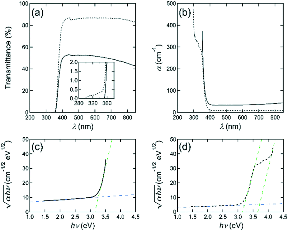 | ||
Fig. 4 (a) The transmittance spectra of single crystal IGZO-11 before (solid line) and after (dotted line) the O2 annealing (1000 °C, 72 hours). The inset in (a) is an enlargement of the region of shorter incident photon wavelength in (a). The thickness of the sample, d is 0.195 mm. (b) The adsorption coefficient α vs. wavelength of the incident photon λ for an as-grown and the post-annealed single crystal, where the adsorption coefficient α was estimated using the relation, α = −ln(T)/d. (c) and (d): The  vs. hν plots for (c) an as-grown and (d) the post-annealed IGZO-11 single crystal. vs. hν plots for (c) an as-grown and (d) the post-annealed IGZO-11 single crystal. | ||
As shown in the inset of Fig. 4(a), a tail-like structure at shorter wavelengths was observed for the post-annealed crystals. This indicates that the oxygen defects may also affect the sub-gap states. By using the relation of α = −ln(T)/d, the absorption coefficient α was calculated and α vs. wavelength of the incident photon λ for an as-grown and the post-annealed single crystal was plotted in Fig. 4(b). One will notice the change in adsorption coefficient before and after the oxygen annealing. So, we need to contemplate the possibility that the detector of the photo-spectrometer reached its sensitivity level limit and small zero-absorption calibration errors (e.g., stray light) may lead to the observed spectral shape. In our U-3010 spectrometer, stray light is less than approximately 0.015% with respect to the reference beam, and our results for the transmittance are in the order of 0.1% in the majority of the region of the tail like structure. In addition, in the case of stray light the transmittance exhibits generally an up-turn-like shape as the wavelength of the incident photon becomes shorter, but this was not observed during our analysis.
Next, in Fig. 4(b), the non-zero absorption coefficient in the wavelength region greater than 400 nm will be not only due to be ignoring the reflectance, but also due to the optical absorption of the free carriers that is stronger in this wavelength range42 as mentioned above. The fundamental absorption edge was estimated as about 370–380 nm for the as-grown crystal and the annealed samples. Fig. 4(c) and (d) show the  vs. hν plots for an as-grown and the annealed IGZO-11 single crystal, respectively, to determine the optical band gap Eg. The optical band gap value was determined from the intersection with the baseline (blue broken-line) in the low photon energy (hν) region of the extrapolation of the linear section (green dotted-lines) of the plot. The value of the optical gap for the as-grown and annealed IGZO-11 single crystals was determined as ∼3.27 eV and ∼3.25 eV, respectively. The slight shift is due to Burstein–Moss effect and suggest that the IGZO-11 single crystal is a degenerate semiconductor and the oxygen defects supply the carriers. In addition, it is important to notice that obvious changes were observed at two locations in the higher photon energy region in the
  vs. hν curve for the annealed samples as shown in Fig. 4(d); one occurs at ∼3.5 eV, and another at ∼4.0 eV, which becomes linear at hν > 4.0 eV. These features originate from the tail-like structure observed in the transmittance spectrum (see the inset of Fig. 4(a)). As shown in Fig. 4(d), the observation of the change of slope at ∼3.5 eV after O2-annealing indicates that the deep impurity states, which locates at near the valence band maximum (VBM), induced by oxygen defects became smaller. However, the new linear part (hν > 4 eV) is a feature that appears from a very small transmittance portion, which is near our detector's sensitivity level limit, so this observation will be regarded as a measurement artifact.
3.2. Electrical transport properties
Fig. 5(a)–(c) show the Arrhenius plots of the in-plane electrical conductivity σab(T), the carrier density ne(T) and the Hall mobility μe(T) of the bulk IGZO-11 single crystals, where it was confirmed from the sign of the Hall coefficient that the charge carriers are electrons. The σab(T) for as-grown IGZO-11 single crystals exhibits almost T-independent behaviour, so called degenerate conduction. The σab(300 K) of the as-grown IGZO-11 is in the range of 300–2000 S cm−1, and the σab(300 K) values can be controlled by careful selection of both the annealing temperature (Tanneal) and annealing time, that is, we can control the σab(300 K) value to within the range of 0.9–200 S cm−1 (see Fig. 5(a)). Here, the origin of the scattering of the σab(300 K) value, is likely to be related to the amount of oxygen vacancies and the disorder of the conducting layer [InO2]− such as anti-site defects. | ||
| Fig. 5 Arrhenius plots of (a) the in-plane electric conductivity σab(T), (b) the carrier density ne(T) and (c) the hall mobility μe(T) for bulk IGZO-11 single crystals. Inset in (a): The annealing temperature (Tanneal) effect of the σab of IGZO-11, where the Tanneal for purple and red circles are 800 and 1000 °C, respectively, and the annealing time for both samples was fixed at 10 h. | ||
The effect of the Tanneal is shown in the inset of Fig. 5(a), where samples with almost the same σab(300 K) were used, and the annealing time was fixed at 10 h. From the inset of Fig. 5(a), one may notice that the higher Tanneal induces a larger change in σab(T), revealing that bulk IGZO-11 single crystals have good controllability for carrier generation. This characteristic is a property suitable for device application. In addition, when the σab(300 K) becomes less than 50 S cm−1 by O2-annealing, the σab(T) shows thermally activated behaviour as shown in Fig. 5(a).
The temperature dependence of the carrier density ne(T) is shown in Fig. 5(b), where ne(300 K) of the IGZO-11 single crystals is in the range of 7 × 10¹⁷ to 6 × 1019 cm−3, and ne(T) exhibits almost T-independent behaviour. However, the mobility μe(T) decreases with decreasing T, when μe(300 K) < 20 cm2/(Vs) which roughly corresponds to ne(300 K) ≲ 1019 cm−3. However, when ne(300 K) exceeds ∼1019 cm−3, the behaviour of μe(T) changes to T-independent behaviour, suggesting degenerate conduction as seen in Fig. 5(c).
The qualitatively similar behaviour of ne(T), σab(T) and μe(T) has been reported for single-crystalline thin films of InGaO3(ZnO)5 (=sc-IGZO-15), but the threshold value of the carrier density nth(300 K) between the degenerate conduction and T-dependent conduction is different, where the nth(300 K) of IGZO-15 films was ∼3 × 1018 cm−3,27 but the nth(300 K) of IGZO-11 bulk single crystals was ∼1019 cm−3. Concerning to the difference of nth(300 K) between the two kinds of samples, this is likely to be due to the number of ZnO layers and/or the difference in type of sample (i.e. thin films or bulk single crystals).
Given the layered structure of IGZO-mn, it is expected that IGZO-mn exhibits anisotropic electrical properties since nonrelativistic first-principles calculations43 show that the electronic structure of IGZO-11 is two dimensional. The electronic state at the edge of the conduction band is formed by an overlap between the In-5s orbitals. The doped electrons are delocalized in the InO2 layer, but the energies of Ga-4s and Zn-4s bands are too high to be doped with electrons.43 However, conductivity along the c-axis (σc) has not yet been reported. Fig. 6 shows the representative T-dependence of σab and σc of as-grown IGZO-11 single crystals, where both each σab and σc were measured using the same fragment of crystal, and then compared. The magnitude of σc at 300 K was in the range of 0.2 to ∼50 S cm−1, which is considerably smaller than the σab(300 K) of the as-grown single crystals. However, the σab and σc values at 300 K scatter depending on the quality of the crystals. If we compare the maximum σc and minimum σab for as-grown IGZO-11, the ratio σab/σc is ∼6. However, if we compare σc and σab in the same crystal, the ratio σab/σc becomes more than 40 as shown in Fig. 6 and 7. The ratio becomes larger for crystals with lower σab (which corresponds to a lower carrier concentration) as shown in Fig. 7. Since the conduction bands are mainly formed by the spherical spread In-5s orbitals, where the overlap between In-5s orbitals is large in the direction of the ab-plane. The large overlap brings about highly dispersed conduction bands, that is, small effective mass. However, the In–In distance along the c-axis is much longer than that along the ab-plane. Therefore the overlap of the wave-function is smaller in c-axis direction and results in a large effective mass. This could be the origin of the anisotropic conductivity for IGZO-11 crystals. The result indicates that the anisotropy will be smaller when Zn is replaced by elements of greater atomic number (e.g. Cd etc.). Because not only is the spatial spread of the 5s-orbitals for Cd2+ larger than the 4s-orbitals of Zn2+, but also the energy level of the Cd2+ 5s-orbitals will be deeper than that of Zn2+ by the relativistic effect, and it will be almost same as the energy level of the In3+ 5s-orbitals. That is, the doped electrons will be able to move along the c-axis. In addition, this model indicates the conductivity along c-axis will become worse as n in IGZO-1n increases. However, the relation between the c-axis conductivity and the number of ZnO layers n will be the subject of a later study.
 | ||
| Fig. 6 Comparison of typical conductivities for in-plane (σab) and out of plane (σc) of three as-grown IGZO-11 single crystals. (#A, #B and #C). The anisotropic ratio σab/σc for single crystal #A, #B and #C is more than 40. | ||
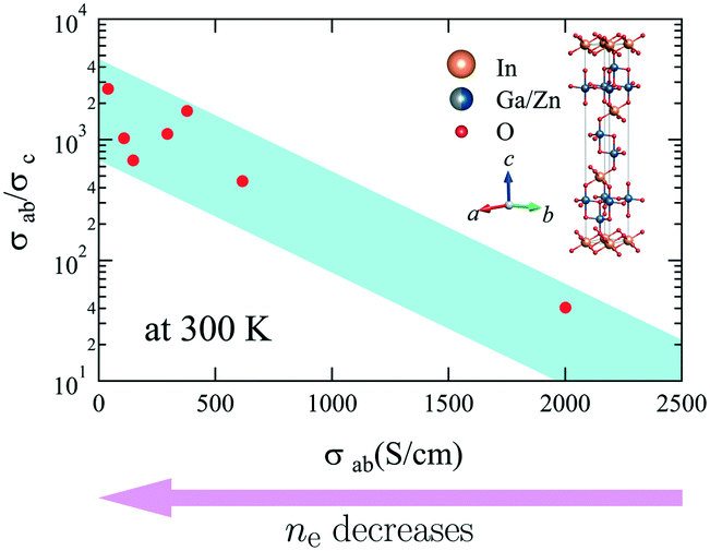 | ||
| Fig. 7 Anisotropy of electrical conductivity in bulk IGZO-11 single crystals at 300 K together with a schematic crystal structure of IGZO-11. The anisotropic ratio, σab/σc increases with lowering σab. | ||
As Kamiya et al. reported, the carrier transport properties of In–Ga–Zn–O thin films show some unusual characteristics.33,44 These include (i) the Hall mobility increases with increasing carrier density, which is the opposite of the standard behaviour for single crystalline semiconductors such as β-Ga2O3. (ii) The maximum Hall mobility of a-IGZO film is almost the same as that of the crystalline thin films. Therefore, it is important to investigate if these unusual characteristics can be observed for bulk single crystals. In other words, are these properties intrinsic features of IGZOs? Therefore, μe(300 K) of bulk IGZO-11 single crystals was re-plotted as a function of ne(300 K) as shown in Fig. 8, where data for a-IGZO,9,45 sc-IGZO-11,44 sc-IGZO-15,9,27 polycrystalline (pc) IGZO thin films27 as well as bulk pc-IGZO-1112 are also plotted for comparison. Concerning the properties of (i) unusual relation between μe(300 K) vs. ne(300 K), although it is believed that this unusual behaviour is typical for the thermally activated conductivity observed in amorphous semiconductors (e.g. amorphous In–Zn–O46 and a-IGZO9,45), our bulk single crystals also exhibited the same behaviour. In addition, some sc-IGZO films have also exhibited the same behaviour.9,27,44 However, the Hall mobility of the bulk single crystals is larger than those of a-, sc-IGZO-1n films and pc-IGZO-11, when ne(300 K) exceeds ∼1019 cm−3, where the sample exhibits degenerate conduction. The origin of this difference will be due to the grain boundaries and/or the decrease of relaxation time by the disorder of the conducting layer [InO2]− such as anti-site defects. These properties suggesting that bulk IGZO single crystals have high potential will be useful in considering device application using IGZO bulk single crystals.
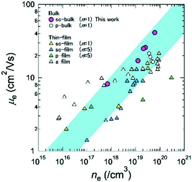 | ||
| Fig. 8 The carrier density dependence of the Hall mobility at 300 K for bulk IGZO-11 single crystals (purple circles). Hall mobilities μe(ne) of bulk IGZO-11 single crystals are compared to those of sc-IGZO-11 films (yellow triangles),44 sc-IGZO-15 films (blue triangles),9,27 a-IGZO films (white triangles),9,45 pc-IGZO films (green triangles)27 and bulk pc-IGZO (white circles).12 | ||
Conclusions
Stoichiometric IGZO-11 single crystals on the centimetre scale have been successfully grown using a high-pressure OFZ technique. Since an IGZO-11 melts incongruently at above 1650 °C, optimum conditions to grow single-phase IGZO-11 require a combination of high-gas pressure and a feed rod with a Zn-rich composition. Bluish, transparent crystals which favour growth perpendicular to the c-axis were obtained. The lattice constants of IGZO-11 grown at higher pressures of 0.8 and 0.9 MPa agree with those of stoichiometric polycrystalline IGZO-11, indicating that the quality of our single crystal is considerably high. Furthermore, XRF results show that the obtained crystals exhibit only a small amount of Zn and In vacancies. The results of the heat treatment clarified the close relationship between absorption of free carriers caused by oxygen vacancies and/or other intrinsic defects, and the crystal's bluish colour. Furthermore, the optical band gap Eg is determined as 3.27 eV for as-grown IGZO-11 single crystal but it became 3.25 eV by Burstein–Moss effect after O2-annealing.The transport properties for bulk IGZO-11 single crystals are summarized as follows: the carrier density ne(300 K) is controllable within the range of 1017–1020 cm−3 at 300 K by post-annealing in an O2 atmosphere. The unusual μevs. ne behaviour (i.e. the increase in μe with increasing ne), which has already been reported in transport studies for some IGZO-1n thin films, was also confirmed for bulk IGZO-11 single crystals. This suggests that the unusual behaviour is an intrinsic characteristic of the IGZO-1n family. However, the values of μe in bulk single crystals are larger than those of sc-IGZO-1n and a-IGZO thin films as well as bulk pc-IGZO-11. In addition, we found that the in-plane conductivity is at least more than 40 times larger than the c-axis conductivity and the anisotropy increases with decreasing carrier density.
Conflicts of interest
There are no conflicts to declare.Acknowledgements
The authors would like to thank Prof. Kensuke Miyajima, Dr. Mario Ohkawa, Prof. Tomohiko Saitoh for their helpful discussions, and Prof. Ryuji Tamura for his help to measure the XRF data, and K. Yoshinaga, K. Tsuji, A. Kamai, Y. Hirochi and M. Shimizu, for their assistance in completing the sample preparation.References
- H. Kawazoe, H. Yanagi, K. Ueda and H. Hosono, MRS Bull., 2000, 25, 28–36 CrossRef CAS.
- N. Kimizuka and T. Mohri, J. Solid State Chem., 1985, 60, 382–384 CrossRef CAS.
- M. Nakamura, N. Kimizuka and T. Mohri, J. Solid State Chem., 1991, 93, 298–315 CrossRef CAS.
- T. Fujii, T. Watanabe and A. Matsuda, J. Cryst. Growth, 2001, 223, 175–180 CrossRef CAS.
- T. Fujii, I. Terasaki, T. Watanabe and A. Matsuda, Phys. Rev. B: Condens. Matter Mater. Phys., 2002, 66, 024507 CrossRef.
- N. Miyakawa, J. F. Zasadzinski, L. Ozyuzer, P. Guptasarma, D. G. Hinks, C. Kendziora and K. E. Gray, Phys. Rev. Lett., 1999, 83, 1018–1021 CrossRef CAS.
- R. Sekine, S. J. Denholme, A. Tsukada, S. Kawashima, M. Minematsu, T. Inose, S. Mikusu, K. Tokiwa, T. Watanabe and N. Miyakawa, J. Phys. Soc. Jpn., 2016, 85, 024702 CrossRef.
- O. Ahmadi, L. Coffey, J. F. Zasadzinski, N. Miyakawa and L. Ozyuzer, Phys. Rev. Lett., 2011, 106, 167005 CrossRef CAS PubMed.
- K. Nomura, H. Ohta, A. Takagi, T. Kamiya, M. Hirano and H. Hosono, Nature, 2004, 432, 488–492 CrossRef CAS PubMed.
- S. Yamazaki, T. Hirohasi, M. Takahashi, S. Adachi, M. Tsubuku, J. Koezuka, K. Okazaki, Y. Kanzaki, H. Matsukizono, S. Kaneko, S. Mori and T. Matsuo, J. Soc. Inf. Disp., 2014, 22(1), 55–67 CrossRef CAS.
- S. Yamazaki, J. Koyama, Y. Yamamoto and K. Okamoto, Dig. Tech. Pap. - Soc. Inf. Disp. Int. Symp., 2012, 43, 183–186 CrossRef CAS.
- M. Orita, M. Takeuchi, H. Sakai and H. Tanji, Jpn. J. Appl. Phys., 1995, 34, L1550–L1552 CrossRef CAS.
- K. Nomura, H. Ohta, K. Ueda, T. Kamiya, M. Hirano and H. Hosono, Science, 2003, 300, 1269–1272 CrossRef CAS PubMed.
- N. Yamada, R. Ino, H. Tomura, Y. Kondo and Y. Ninomiya, Adv. Electron. Mater., 2017, 3, 1700298 CrossRef.
- K. Kato, Y. Shionoiri, Y. Sekine, K. Furutani, T. Hatano, T. Aoki, M. Sasaki, H. Tomatsu, J. Koyama and S. Yamazaki, Jpn. J. Appl. Phys., 2012, 51, 021201 CrossRef.
- M. Tsubuku, D. Matsubayashi, T. Takeuchi, R. Honda, T. Murakawa, S. Matsuda, Y. Yamamoto and S. Yamazaki, ECS Trans., 2015, 67, 17–22 CrossRef CAS.
- Physics and Technology of Crystalline Oxide Semiconductor CAAC-IGZO: Application to Displays, ed. S. Yamazaki and T. Tsutsui, Wiley, U.K., 2017 Search PubMed.
- T. Moriga, D. R. Kammler and T. O. Mason, J. Am. Ceram. Soc., 1999, 82, 2705–2710 CrossRef CAS.
- M. Nespolo, A. Sato, T. Osawa and H. Ohashi, Cryst. Res. Technol., 2000, 35, 151–165 CrossRef CAS.
- W. Assenmacher, G. Schnakenburg, Y. Michiue, Y. Kanke, N. Kimizuka and W. Mader, J. Solid State Chem., 2014, 215, 176–183 CrossRef CAS.
- H. Ohta, K. Nomura, M. Orita, M. Hirano, K. Ueda, T. Suzuki, Y. Ikuhara and H. Hosono, Adv. Funct. Mater., 2003, 13, 139–144 CrossRef CAS.
- M. Isobe, N. Kimizuka, M. Nakamura and T. Mohri, Acta Crystallogr., Sect. C: Struct. Chem., 1994, 50, 332–336 CrossRef.
- Springer Handbook of Crystal Growth, ed. G. Dhanaraj, K. Byrappa, V. Prasad and M. Dudley, Springer, Berlin, Heidelberg, 2010, DOI:10.1007/978-3-540-74761-1.
- J. Zhang, B. Li, C. Xia, J. Xu, Q. Deng, X. Xu, F. Wu, W. Xu, H. Shi, G. Pei and Y. Wu, Sci. China, Ser. E: Technol. Sci., 2007, 50, 51–56 CrossRef CAS.
- I. Tanaka and H. Kojima, Nature, 1989, 337, 21–22 CrossRef.
- A. Murat, A. U. Adler, T. O. Mason and J. E. Medvedeva, J. Am. Chem. Soc., 2013, 135, 5685–5692 CrossRef CAS PubMed.
- K. Nomura, T. Kamiya, H. Ohta, K. Ueda, M. Hirano and H. Hosono, Appl. Phys. Lett., 2004, 85, 1993–1995 CrossRef CAS.
- T. Kamiya, K. Nomura and H. Hosono, Appl. Phys. Lett., 2010, 96, 122103 CrossRef.
- T. Kamiya, K. Nomura and H. Hosono, J. Disp. Technol., 2009, 5, 273–288 CAS.
- H. Yabuta, M. Sano, K. Abe, T. Aiba, T. Den and H. Kumomi, Appl. Phys. Lett., 2006, 89, 112123 CrossRef.
- T. Kamiya and H. Hosono, NPG Asia Mater., 2010, 2, 15–22 CrossRef.
- J. Koezuka, K. Okazaki, T. Hirohashi, M. Takahashi, S. Adachi, M. Tsubuku, S. Yamazaki, Y. Kanzaki, H. Matsukizono, S. Kaneko, S. Mori and T. Matsuo, Dig. Tech. Pap. - Soc. Inf. Disp. Int. Symp., 2013, 44, 723–726 CrossRef CAS.
- Y. Kobayashi, S. Matsuda, D. Matsubayashi, H. Suzawa, M. Sakakura, K. Hanaoka, Y. Okazaki, T. Yamamoto, S. Hondo, T. Hamada, S. Sasagawa, M. Nagai, Y. Hata, T. Maruyama, Y. Yamamoto and S. Yamazaki, Jpn. J. Appl. Phys., 2014, 53, 04EF03 CrossRef.
- C. Y. Chung, B. Zhu, R. G. Greene, M. O. Thompson and D. G. Ast, Appl. Phys. Lett., 2015, 107, 183503 CrossRef.
- H. Godo, D. Kawase, S. Yoshitomi, T. Sasaki, S. Ito, H. Ohara, H. Kishida, M. Takahashi, A. Miyanaga and S. Yamazaki, Jpn. J. Appl. Phys., 2010, 49, 03CB04 CrossRef.
- K. Kato, Y. Shionoiri, Y. Sekine, K. Furutani, T. Hatano, T. Aoki, M. Sasaki, H. Tomatsu, J. Koyama and S. Yamazaki, Jpn. J. Appl. Phys., 2012, 51, 021201 CrossRef.
- S. Yamazaki, ECS Trans., 2013, 54(1), 85–96 CrossRef.
- H. Sato, A. Tsukada, M. Naito and A. Matsuda, Phys. Rev. B: Condens. Matter Mater. Phys., 2000, 62, R799–R802 CrossRef CAS.
- J. Tauc, R. Grigovici and A. Vancu, Phys. Status Solidi, 1966, 15, 627 CrossRef CAS.
- B. D. Viezbicke, S. Patel, B. E. Davis and D. P. Birnie, Phys. Status Solidi B, 2015, 252, 1700–1710 CrossRef CAS.
- T. Kamiya, K. Nomura and H. Hosono, Phys. Status Solidi A, 2009, 206, 860–867 CrossRef CAS.
- Z. Galazka, K. Irmscher, R. Uecker, R. Bertram, M. Pietsch, A. Kwasniewski, M. Naumann, T. Schulz, R. Schewski, D. Klimm and M. Bickermann, J. Cryst. Growth, 2014, 404, 184–191 CrossRef CAS.
- M. Orita, H. Tanji, M. Mizuno, H. Adachi and I. Tanaka, Phys. Rev. B: Condens. Matter Mater. Phys., 2000, 61, 1811–1815 CrossRef CAS.
- T. Kamiya, K. Nomura and H. Hosono, Sci. Technol. Adv. Mater., 2010, 11, 044305 CrossRef PubMed.
- A. Takagi, K. Nomura, H. Ohta, H. Yanagi, T. Kamiya, M. Hirano and H. Hosono, Thin Solid Films, 2005, 486, 38–41 CrossRef CAS.
- A. J. Leenheer, J. D. Perkins, M. F. A. M. van Hest, J. J. Berry, R. P. O'Hayre and D. S. Ginley, Phys. Rev. B: Condens. Matter Mater. Phys., 2008, 77, 115215 CrossRef.
Footnotes |
| † Electronic supplementary information (ESI) available: X-ray diffraction data of (S1) a vaporized substance from the molten zone during the crystal growth, (S2) a grown crystal by the OFZ method under normal pressure, (S3) crystals grown by various conditions (the effect of gas pressure and composition of a feed rod. See DOI: 10.1039/c9ce00007k |
| ‡ Department of Applied Electronics, Tokyo University of Science, 6-3-1 Niijuku, Katsushika-ku, Tokyo 125-8585, Japan. |
| This journal is © The Royal Society of Chemistry 2019 |