
 Open Access Article
 This Open Access Article is licensed under a
 Creative Commons Attribution 3.0 Unported Licence
Superlattices based on van der Waals 2D materials
Yu Kyoung
Ryu
 *,
Riccardo
Frisenda
and
Andres
Castellanos-Gomez
*
*,
Riccardo
Frisenda
and
Andres
Castellanos-Gomez
*
Materials Science Factory, Instituto de Ciencia de Materiales de Madrid (ICMM-CSIC), Madrid, E-28049, Spain. E-mail: yukyoung.ryu@csic.es; andres.castellanos@csic.es
First published on 15th August 2019
Abstract
Two-dimensional (2D) materials exhibit a number of improved mechanical, optical, and electronic properties compared to their bulk counterparts. The absence of dangling bonds in the cleaved surfaces of these materials allows combining different 2D materials into van der Waals heterostructures to fabricate p-n junctions, photodetectors, and 2D–2D ohmic contacts that show unexpected performances. These intriguing results are regularly summarized in comprehensive reviews. A strategy to tailor their properties even further and to observe novel quantum phenomena consists in the fabrication of superlattices whose unit cell is formed either by two dissimilar 2D materials or by a 2D material subjected to a periodic perturbation, each component contributing with different characteristics. Furthermore, in a 2D material-based superlattice, the interlayer interaction between the layers mediated by van der Waals forces constitutes a key parameter to tune the global properties of the superlattice. The above-mentioned factors reflect the potential to devise countless combinations of van der Waals 2D material-based superlattices. In the present feature article, we explain in detail the state-of-the-art of 2D material-based superlattices and describe the different methods to fabricate them, classified as vertical stacking, intercalation with atoms or molecules, moiré patterning, strain engineering and lithographic design. We also aim to highlight some of the specific applications of each type of superlattices.
 From left to right: Andres Castellanos-Gomez, Yu Kyoung Ryu and Riccardo Frisenda | Our lab is part of the 2D Foundry, a research group of the Instituto de Ciencia de Materiales de Madrid (which is part of the Spanish National Research Council, Consejo Superior de Investigaciones Científicas). Our research focusses on the exploration of novel 2D materials and the use of strain engineering to modify their properties. Through the fabrication of optoelectronic nanodevices based on 2D materials, heterostructures and superlattices we probe the electronic, mechanical and optical properties of these nanomaterials. We also devote a fraction of our research time to develop experimental techniques and cost-effective tools to make 2D materials research more accessible and widespread. |
1. Introduction
In their Communication (1970), IBM researchers Esaki and Tsu envisioned theoretically the realization of a novel semiconductor structure,1 either by a periodic variation of the doping level in a single material or by a periodic variation of two dissimilar materials. They claimed that if the period of such structures was shorter than the electron mean free path, it would be possible to observe new quantum confinement phenomena, due to the opening of extra allowed and forbidden energy bands, not available in a traditional device. They coined this novel device with a periodic potential as “superlattice”. Shortly after, Esaki and Chang demonstrated quantum transport states in a 50-period GaAs–AlAs superlattice fabricated by molecular-beam epitaxy.2 Later, Osbourn introduced strain-engineering as a new variable to modulate the bandgap in a superlattice by controlling the growth of alternative layers with a certain lattice mismatch.3 In these pioneering works, the authors had predicted that the experimental evolution of superlattices would mean the opening of new fields in semiconductor research. Since then, the semiconductor industry has developed standard fabrication methods to obtain superlattices from conventional 3D semiconducting materials through molecular beam epitaxy, sputtering or other vacuum deposition methods.4–6 These conventional superlattices have reached a limitation in their thermoelectric, optoelectronic, and energy-storage performance that does not meet the current needs of the society. On this basis, the nanowires, due to their reduced dimensions and high surface-to-volume ratio, are being considered as new building blocks for the next generation of superlattices.7–9 Nevertheless, the control over the interface states to obtain an optimal, abrupt junction is difficult due to the covalent nature of most of the nanowire heterojunctions and the presence of dangling bonds in their surface.10The isolation of 2D materials by mechanical or chemical exfoliation of bulk van der Waals materials and the synthesis of ultrathin van der Waals layered materials have changed one step further the paradigm in the fabrication of superlattices. 2D materials are atomically thin and have an area on the order of hundreds of microns square. This trait endows them with an extremely high surface-to-volume ratio. The surface of these materials is devoid of dangling bonds and their heterostructures are held by van der Waals forces. As a result of these features, 2D materials have shown extraordinary physical and chemical properties. This has motivated the synthesis of novel 2D nanomaterials such as ultrathin metal–organic framework layers,11 transition metal oxides and hydroxides12 or covalent-organic framework layers,13,14 in order to obtain enhanced chemical reactivity and device performance in comparison to their 3D, covalent homologues. This wide variety of 2D nanomaterials and available methods to prepare them open the door to the emerging field of van der Waals superlattices. Starting with 2D materials as the building blocks, periodic potentials from structures with precise atomic resolution can be now easily achieved, even without the need of vacuum deposition techniques. The exploration of superlattices based on van der Waals 2D materials, both theoretically and experimentally, has barely started. However, there exists already a solid body of results that contributes to settle down the bases of the field. These results are the focus of the present feature article, divided into the main 2D based superlattice types shown in Table 1:
| Classification | Elements of the unit cell | Modulation by (dimension) | Applications (ref.) |
|---|---|---|---|
| Vertical stacking |
|
Chemical composition, lattice (mis)match (1D) | • IR photodetectors15,16,20 |
| • Phase-change memory28–34 | |||
| • Thermoelectrics47–50 | |||
| • Superconductivity51–54 | |||
| Intercalated compounds |
|
Chemical composition, structuring, charge transfer (1D) | • Optoelectronics55–61,72–75 |
| • Superconductivity62 | |||
| • Thermoelectrics63,64 | |||
| • Energy storage67–71 | |||
| Moiré periodic patterns |
|
Atom rearrangement, misorientation angle, strain (2D) | • Dirac point states87,95–99 |
| • Hofstadter's butterfly89–94 | |||
| • Superconductivity100–106 | |||
| • Moiré interlayer excitons107–109 | |||
| Strain engineered |
|
Periodic in-plane or out-of-plane strain (1D or 2D) | • Phase-change memory117,118 |
| • Bandgap engineering119–122 | |||
| • Optoelectronics125,126 | |||
| Lithographic engineered |
|
Dielectric patterning, periodic substrate, periodic patterning, strain (1D or 2D) | • Artificial crystals128–130 |
| • Moiré periodicities131 | |||
| • Bandgap engineering132,133 |
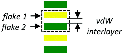
(1) Vertical stacking of dissimilar 2D layers, where the periodic potential is modulated principally by the chemical composition of the layers and/or the lattice mismatch existing between them.
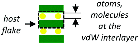
(2) Multi-layered 2D materials that are subjected to an intercalation process. In this type of superlattices, the periodic potential can be modulated by the chemical composition of the layers, the re-structuration of the functionalized layers after the intercalation of the hosting species and the charge transfer that takes place between the host flakes and the atoms or molecules.
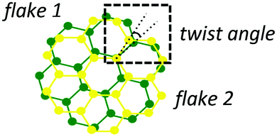
(3) Moiré structures by twisting of two 2D material-based layers. When two equivalent (e.g. graphene bilayer) or dissimilar (e.g. graphene/h-BN) adjacent layers are rotated under certain angles, the lattice mismatch and/or the atom rearrangement give rise to moiré-pattern superlattices with new lattice periodicities.
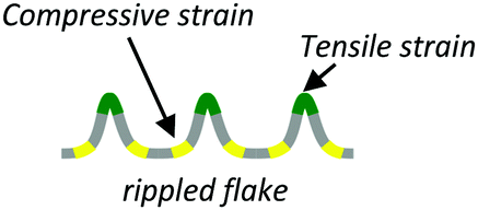
(4) Strain-engineered layers. A periodic potential can be produced by subjecting a 2D material flake to periodic tensile/compressive strains or by introducing a periodic, controlled mismatch between the lattices of two dissimilar 2D materials.
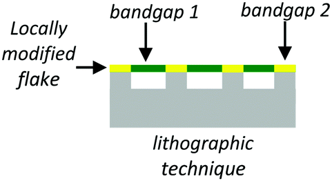
(5) Synthetic superlattices defined by lithography. In this approach, the periodic potential can be induced in a 2D material by placing it on a patterned topography or by patterning the material itself with a lithographic technique.
Note that in some cases there is more than one single mechanism involved in the fabrication of the superstructure. Specifically, either as an explicit parameter or produced unintentionally, strain is found to have an important role in the modulation of electronic/optical properties in most of the other types of superlattices.
Each type of superlattice (1 to 5) and its potential applications will be discussed in detail in the next section and the corresponding subsections.
2. 2D material superlattices
2.1 Vertically stacked superlattices
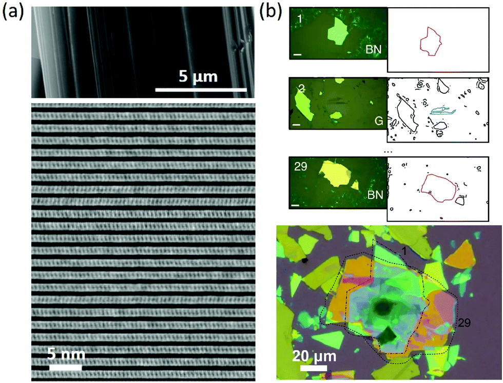 | ||
Fig. 1 (a) SEM image of an exfoliated franckeite showing the layered nature of the mineral (top). Cross-sectional TEM image of the superlattice viewed along the [100] direction. Reproduced with permission from ref. 5. (b) Artificial van der Waals superlattice comprising 29 alternating layers of graphite and h-BN. Top: Optical microscope images of some of the graphite (G) and BN flakes utilized to assemble the superlattice (left) and the vector-drawing line-edges of the flakes automatically extracted from the optical microscope images. The scale bars correspond to 20![[thin space (1/6-em)]](https://www.rsc.org/images/entities/char_2009.gif) μm. Bottom: Optical image of the G/BN superlattice. The dashed lines highlight the bottom and top BN flakes. Reproduced with permission from ref. 12. μm. Bottom: Optical image of the G/BN superlattice. The dashed lines highlight the bottom and top BN flakes. Reproduced with permission from ref. 12. | ||
Interfacial phase-change memory materials that encompass the family of superlattices with the general formula [(GeTe)x/(Sb2Te3)y]n are being studied to achieve fast switching and low energy consumption for non-volatile memory applications.28 The TEM characterization of GeTe/Sb2Te3 superlattices fabricated by MBE and annealed at 400 °C revealed a reorganization of the superlattice structure into Sb2Te3 and GeSbTe rhombohedral layers.29 The prediction of the authors about modulating the electrical, thermal or magnetic properties by controlling the MBE process in this kind of materials was accomplished by Cecchi et al.30 The authors fabricated by molecular beam epitaxy Sb2Te3/GexSb2Te3+x superlattices. They observed that this configuration reduced the intermixing of the layers compared to the standard GeTe/Sb2Te3 superlattices fabricated in the previous work.29 As a consequence, superlattices with less defective, sharper interfaces and higher carrier mobility were achieved. Another epitaxial method, radio-frequency sputtering, has been employed to fabricate interfacial phase-change memory superlattices in several works.31–34 Particularly, the phase change from a Dirac semimetal to a topological insulator as a function of the thickness of the GeTe layer has been observed, which is promising for spintronic applications.34
In the case of natural minerals such as franckeite15,16 and cylindrite,20 it was shown how the alternating formation of layers with dissimilar lattice symmetry gives rise to superlattices that grow with a mismatch, but are ordered and thermodynamically stable. This type of materials, called misfit layer compounds, can be synthesized with controlled properties as well. Their general formula is [(MX)1+δ]m(TX2)n, where M = Sn, Pb, Bi, Sb, rare earths; T = Ti, V, Nb, Ta, Cr; and X = S or Se.35,36 There is a variant of misfit layer compounds that is metastable and exhibits a turbostratic or rotational disorder along the c-axis, called ferecrystals. These materials present the general formula [(MX)1+δ]m(TX2)n, where M = Sn, Pb, Bi, La; T = Ti, V, Nb, Ta, Cr, Mo, W; and X = S, Se or Te.35–38 In both formulas, the coefficients m and n represent the number of layers of each material per unit cell. In a misfit layer compound, there is only one axis of the layers that presents an incommensurate crystallographic direction (Fig. 2(a), left, from ref. 36), while both in-plane axes of the layers in a ferecrystal are incommensurate and independent of each other (Fig. 2(a), right, from ref. 36). The dimensionality (m layers of material 1 and n layers of material 2 per unit cell, i.e. their ratio m/n) of these materials is taken into account to control the properties of both materials: the electrical transport,39–41 the charge transfer between the layers42,43 or the presence/strength of a charge density wave state.44 Another strategy followed to modulate the electrical properties is by substitution or doping in specific sites of the layers.45–47
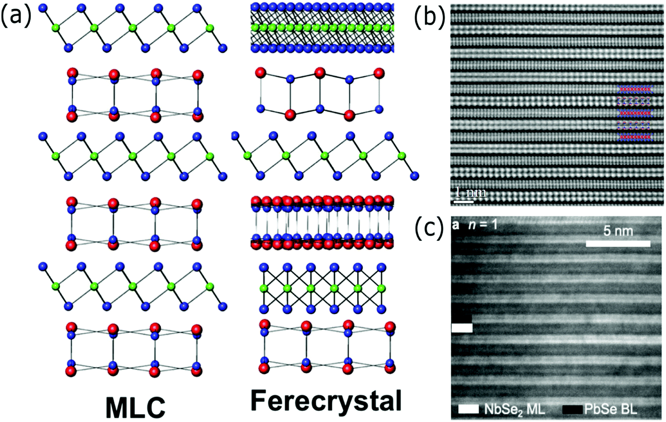 | ||
| Fig. 2 (a) Scheme of the superlattice structure of a misfit layered compound (MLC, left) and a ferecrystal (right). Reproduced with permission from ref. 25. (b) High resolution TEM image of a (SnSe)1.16(NbSe2) MLC superconducting superlattice, viewed along the [010] direction. The inset is a scheme of the SnSe/NbSe2 layers. Reproduced with permission from ref. 40. (c) Cross-sectional TEM image of a (PbSe)1.14(NbSe2)n ferecrystal superconducting superlattice with n = 1. Reproduced with permission from ref. 42. | ||
Both misfit layer compounds and ferecrystals present a high potential in thermoelectric applications because their structure is ideal to develop phonon glass/electron crystal responses, where dichalcogenide layers with high electrical mobility constitute the electron crystal component while the mismatch or turbostratic disorder along the c-axis lowers the lattice thermal conductivity, acting as the phonon glass.36,48,49 The recent work by Li et al.50 demonstrated the influence of the cross-plane thermoelectric properties as a function of the thickness of the layers that formed a misfit layer compound superlattice. The authors measured devices based on (SnSe)n(TiSe2)n, varying the number of layers by n = 1, 3, 4, 5, but keeping the same global stoichiometry. They observed a quasi-linear increase in the cross-plane Seebeck coefficient from −2.5 to −31 μV K−1 as a function of n, and an approximately constant in-plane Seebeck coefficient for different values of n. Another strategy to improve the thermoelectric properties has been the Cu- and Co-substitution of Ti-sites in the TiS2 layers of a (SnS)1.2(TiS2)2 misfit-layered compound. An increase of the ZT value up to 33.3% in (SnS)1.2(Cu0.02Ti0.98S2)2 was obtained compared to the pristine misfit layer compound. This improvement of the figure of merit was explained in terms of the increase in the effective mass and the decrease in the carrier concentration induced by Cu incorporation and the decrease in the thermal conductivity induced by the disorder inherent to the misfit layer compound structuring.47
Superconductivity is another application barely explored yet in both misfit layer compounds and ferecrystals. Superconductivity in the synthesized misfit layer compounds (SnSe)1.16(NbSe2)51 and (SnS)1.15(TaS2)52 with critical temperatures (Tc) of, respectively, 3.4 and 3.01 K was recently reported. In the (PbSe)1.14(NbSe2)n ferecrystal,53 the shift of Tc from 2.66 (n = 3), 1.91 (n = 2) and 1.11 (n = 1) K was observed. The authors studied the reduction of the transition temperature as a function of the thickness of the ferecrystal unit cell, since the electron-phonon coupling and the interlayer charge transfer are modulated by the number of layers (n). The control of the transition temperature by varying the m index instead in a [(SnSe)1+δ]m(NbSe2) ferecrystal has also been observed.54Fig. 2(b) and (c) show, respectively, the cross-sectional TEM images of a misfit layer compound51 and ferecrystal53 superconducting superlattice.
To summarize this section, the composition of the unit cell in terms of the number of layers and crystalline phase of each material determines the coupling and charge transfer between layers, which are the factors that most influence the thermoelectric and electronic properties of this type of superlattices.
2.2 2D material layer-intercalated compound superlattices
In the previous section, it was discussed how the interlayer interactions between the layers that are part of a vertical stacking have a big influence on the cross-plane properties of the superlattice. Therefore, the coupling between layers for each system was adjusted by controlling the thickness, the doping and the crystallographic structure of the constituents. This peculiar interlayer spacing characteristic of van der Waals layered materials is found to have a considerable impact on the optical and electrical properties of the devices fabricated by or involved in intercalation methods. This section will review the works where ions or molecules were intercalated between the layers of a 2D material forming a different kind of superlattice.A simultaneous enhancement in both the optical transmission and the electrical conduction through the phase change underwent by a 2D material after intercalation has been demonstrated in copper-intercalated bismuth-based chalcogenide layers.55,56 The effect of Li intercalation on the charge density in different van der Waals heterostructures has been recently studied.57 The tuning of the electrical and optical properties through intercalation has been also observed in ammonia ions-WS2 host,58 lithium ions-NbSe2 host,59 cetyl-trimethylammonium bromide (CTAB) in black phosphorus (BP),60 and tetraethylbenzidine (EtDAB) ions in PbI2.61 In a recent work, the coexistence of superconductivity and ferromagnetism originated from non-superconducting and non-ferromagnetic components has been achieved by the fabrication of a two-dimensional SnSe2/Co(Cp)2 superlattice, where Cp represents cyclopentadienyl molecules. A TEM cross-section of the superlattice is shown in Fig. 3(a) (left). The confinement effect that the Co(Cp)2 molecules experience when they are sandwiched between the SnSe2 layers weakens their coordination field, inducing the high spin ferromagnetic state (scheme in Fig. 3(a), right). The strong interlayer coupling between the Cp molecules and the SnSe2 lattice induces a superconducting state through an unusual electron transfer.62
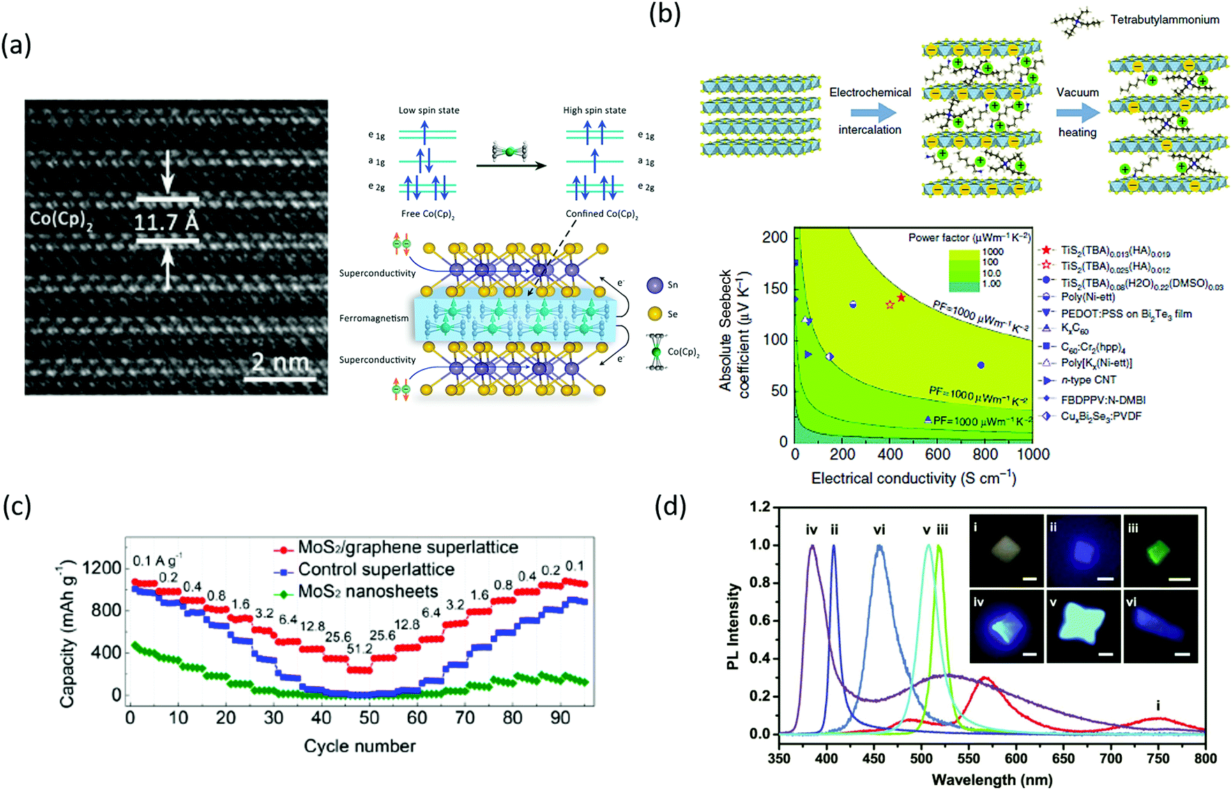 | ||
| Fig. 3 (a) Cross-sectional TEM image of the SnSe2-Co(Cp)2 superlattice (left). Scheme where the unit cell of the superlattice is shown, as well as the induced high spin state in the Co(Cp)2 molecules when they are confined between the SnSe2 layers (right). Reproduced with permission from ref. 51. (b) Scheme of one of the fabricated superlattices after electrochemical intercalation of hexylammonium/tetrabutylammonium molecules and vacuum heating (top). The absolute Seebeck coefficient represented as a function of the electrical conductivity shows that the intercalated TiS2 compounds have a higher power factor compared to other thermoelectric materials (bottom). Reproduced with permission from ref. 52. (c) Rate capability as a function of cycling number of the 1T MoS2/graphene superlattice is higher compared to control devices (1H MoS2/graphene superlattice) and MoS2 nanosheets. Reproduced with permission from ref. 57. (d) PL spectra of different 2D hybrid perovskites (corresponding to the crystals shown in the optical PL images of the inset). By optimizing the conditions of the same synthesis process, it is possible to achieve crystals with different wavelengths in the visible. Reproduced with permission from ref. 64. | ||
In the previous section, we discussed how the interlayer disorder found in misfit layer compounds and ferecrystals could be controlled to optimize the carrier mobility and reduce the thermal conductivity to achieve high ZT for thermoelectric applications. Wan et al.63–65 employed another approach to achieve a similar effect in TiS2. The authors intercalated at the interface of TiS2 thin layers organic cations such as hexylammonium ions (HA) and polar organic molecules such as dimethyl sulfoxide (DMSO). A scheme of the fabrication process is shown in Fig. 3(b) (top).65 The reason behind was to engineer the dielectric constant between the two-dimensional TiS2 layers to optimize the electrical mobility/thermal conductivity ratio. With this hybrid inorganic–organic superlattice structure, the authors obtained a thermal conductivity 7 times lower compared to that of TiS2 single crystals.64 A further improvement of this process led to the attainment of a power factor of 904 μW m−1 K−2, considerably higher compared to other thermoelectric materials, as shown in Fig. 3(b) (bottom).65
There is a research effort devoted to optimize 2D material superlattices for energy storage applications.66 In a smart design, MoS2 monolayers were self-assembled by means of dopamine molecules adsorbed on their surface. After annealing, the dopamine layers sandwiched between the MoS2 monolayers were thermally converted into nitrogen-doped graphene. This fabrication process results in a superlattice-like structure with good anode performance for lithium ion batteries. The fast charge–discharge rate and high cycling stability are attributed to the increase of reactive sites inherent to the new structure and an intimate interfacial coupling that enhances the electric and charge transfer.67 In Sasaki's group, a superlattice based on metallic 1T-MoS2/graphene monolayers has been fabricated by Li intercalation and solution-phase direct assembly. This superlattice was used as an anode for sodium ion batteries. It showed a larger capacity performance compared to the MoS2 nanosheets and the 1H-MoS2 monolayer/graphene monolayer superlattice (Fig. 3(c)) and a long-term stability up to 1000 cycles.68 The same group has demonstrated the superior performance of metal oxide based anodes for lithium or sodium ion batteries when they are integrated in a van der Waals stacking superlattice. Two-dimensional metal oxides and hydroxides present optical properties and rich redox states that make them promising for energy storage applications. The authors fabricated a superlattice based on intercalated MnO2 monolayers/graphene monolayers. The hybridization of the MnO2/graphene monolayers resulted in enhanced conductivity, achieving faster charge transport, a larger specific capacity and long-term stability up to 5000 cycles.69 In a third approach, the same authors fabricated a Ti0.87O2 monolayer/graphene monolayer superlattice as an anode for sodium ion batteries, where the titanium oxide layer was synthesized with Ti vacancies to increase the number of redox active sites and the graphene layer to enhance the conductivity.70 When layered double hydroxide layers are inserted between MoS2 monolayers, the strong interaction that takes place at the interface strengthens their electronic coupling, and thus, improves the electrical and charge transfer. As a result, the superlattice acts as a catalyst for overall water splitting.71
The achievement of improved performance or novel phenomena from a given two-dimensional material by tuning its dimensionality and/or intercalating organic molecules in the interlayer space is also followed by the hybrid organic–inorganic perovskite field. Efficient blue LEDs at room temperature were fabricated from two-dimensional (RNH3)2[CH3NH3PbX3]nPbX perovskites by (a) controlling the stacking number that gives rise to blue shift by quantum confinement and (b) designing dielectric quantum wells with organic host compounds to enhance the exciton binding energy and boost radiative recombination.72 The control of the layer thickness in Ruddlesden–Popper type of perovskites, with the general formula of (RNH3)2(CH3NH3)n−1MnX3n+1, has been studied to change the bandgap for achieving photodetectors with tunable wavelength73–75 and to tune the cross-plane acoustic phonon transport.76 In Fig. 3(d) we have presented the tunability of the wavelength as a function of the composition of 2D perovskites fabricated with the same synthesis process.75 The level of anisotropy as a function of the n inorganic layers in a 2D EA2MAn−1PbI3n+1 perovskite, where EA = HOC2H4NH3+ and MA = CH3NH3+, was studied. The two dimensional perovskite with n = 1 and layer-edge 0° device displayed a humidity sensitivity almost four orders of magnitude higher than that of the 3D homologous perovskite.77
In this section, ions and molecules intercalated between the layers of the host 2D material were the elements employed to modulate the interlayer coupling and charge transfer to obtain superlattices with improved electronic, optical and thermoelectrical properties and to enhance the chemical reactivity, fundamental for energy-storage applications.
2.3 Moiré superlattices
The main approach to obtain moiré superlattices is the stacking of two 2D layered materials with a controlled rotation angle or lattice mismatch. These two materials can be equal, such as in the case of a twisted double-layer graphene78 or the creation of a moiré superlattice from the rotation of the topmost layer of a Bi2Te3 quintuple layer.79 Nevertheless, another common moiré superlattice is created by the stacking and twisting of two different materials, such as graphene on hexagonal boron nitride (h-BN),80 or by van der Waals epitaxial growth of one of the materials over the other, such as Bi2Se3 on h-BN,81 GaSe monolayer on MoSe2 monolayer,82 MoS2 monolayer on WSe2 monolayer83 and SnS2 monolayers on WSe2 monolayers.84 Recently, the creation of a third moiré superlattice with a larger potential period from the overlap of the bottom and top moiré superlattices in a h-BN/graphene/h-BN system was demonstrated.85The number of novel quantum phenomena observed experimentally in graphene/h-BN moiré superlattices is impressive and it is increasing fast. We refer the readers interested in more details about this topic to a recent review.86 The periodic potential created by the lattice mismatch between graphene and h-BN gives rise to new Dirac points whose energy depends on the wavelength of the moiré potential.87 Two dimensional electrons under the simultaneous application of a magnetic field and a periodic electrostatic potential display a fractal-like quantized energy spectrum called Hofstadter's butterfly.88 In 2013, Hofstadter's butterfly was observed experimentally on graphene/h-BN lattices with small angle mismatches in the range of 4°–15° by three different groups.89–91 A scheme of the device and the experimentally observed Hofstadter's butterfly spectra are shown in Fig. 4(a).89 Later, one of these groups proved the coexistence of fractional quantum Hall effect states with integer states associated with Hofstadter's butterfly spectrum and the apparition of novel fractional Bloch quantum Hall effect states at high magnetic fields.92 With these results, the complete unit cell of the butterfly spectrum is covered. Another of these groups have studied further the novel Bloch states that lead to quantum oscillations, associated to Hofstadter's butterfly.93,94 The commensurate stacking leading to topological bands and the incommensurate stacking leading to non-topological bands (due to the inhomogeneous potential landscape induced by the moiré pattern) can be achieved by controlling the twist angle between graphene and h-BN.95,96 A gate-tunable Mott insulator was demonstrated by varying the bandgap of an h-BN/trilayer graphene/h-BN moiré superlattice with a vertical electric field.97 Novel plasmonic modes arisen from the Dirac mini-bands found in the moiré superlattice were observed.98 Electron tunnelling spectroscopy was used to measure the energy gaps formed at the first and second Dirac points of mono- and bilayer graphene/h-BN moiré superlattices as a function of twist angles and external electric and magnetic fields.99
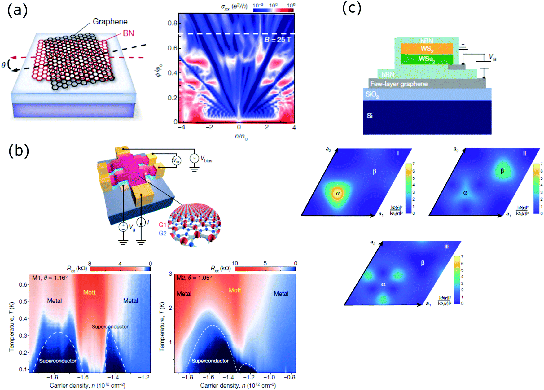 | ||
| Fig. 4 (a) Scheme of the twisted graphene and h-BN at an angle θ. The moiré wavelength can be designed as a function of θ (left). Hall conductivity σxx as a function of the normalized magnetic flux per unit cell and carrier density. A Hofstadter's butterfly with its characteristic fractal behaviour is displayed (right). Reproduced with permission from ref. 78. (b) Scheme of a twisted bilayer graphene fabricated as a 4-probe Hall bar device (top). 4-Probe resistance Rxx measured as a function of the temperature and carrier density for two different twist angles, 1.05° and 1.16°, very close to the ‘magic angle = 1.1°’. Both graphs show superconducting behaviour (bottom row) under the two angles, with variations in the superconducting domes. Reproduced with permission from ref. 90. (c) Scheme of the device, where the transition metal dichalcogenide monolayers have a twist angle close to zero (top). Real-space distribution of exciton centre-of-mass wavefunction. These maps show the apparition of three different moiré minibands (states I–III) in the strong-coupling regime (middle and bottom row). With permission from ref. 97. | ||
Although it was predicted theoretically in 2011,100 the experimental observation of unconventional superconductivity in two graphene layers twisted by a magic angle of about 1.1° in 2018, by Jarillo-Herrero's group, has shaken up the physics community. Fig. 4(b) shows the 4-probe resistance Rxx measured as a function of the carrier density and the temperature for two different devices. Both devices with the magic angles of 1.16° and 1.05°, respectively, display two superconducting domes, overlapped in the second case.101 This work has boosted the emergence of the twistronics field,102,103 where all the rich electronic properties and range of magical angles in graphene twisted double-layers are being investigated.104–106 On the other hand, the possibility to extend the study to other van der Waals layers twisted at small angles in order to produce novel collective excitation behaviours was soon realized. Different research groups have observed moiré interlayer excitons in MoSe2/MoS2,107 WSe2/WS2108 and MoSe2/WSe2109 moiré superlattices. Jin et al. fabricated a fully h-BN encapsulated WSe2/WS2 heterostructure, with a measured twist angle of 0.5 ± 0.3° (Fig. 4(c), top). At the strong-coupling regime of a large moiré potential, three moiré exciton minibands appeared, represented in Fig. 4(c), since under this regime the moiré potential is stronger than the exciton kinetic energy.108
The influence of the interlayer interface on the physical properties is common in all types of two-dimensional van der Waals superlattices. A scanning tunnelling microscopy tip was employed to apply pressure on a graphene/h-BN superlattice, controlling the interlayer distance between the layers. It was demonstrated that the degree of commensurate stacking and the in-plane strain of graphene can be controlled as a function of the interlayer distance, tuning the electronic properties.110 A laser induced shocking wave was used to eliminate wrinkles, bubbles and residues in the interlayer spaces of graphene/BN/graphene moiré superlattices. This produced a reduction of the interlayer distance between the graphene layers and the boron nitride and an enhancement in the interlayer electron coupling. As a consequence, an opening of a small bandgap was observed.111 It has been predicted theoretically that by controlling the interlayer hybridization, a mosaic pattern with local topological insulator areas and normal insulator areas in moiré superlattices was formed by two massive Dirac materials.112
The results explained in this section show how an in-plane periodic potential can be introduced by stacking materials with a certain lattice mismatch or by twisting two 2D material layers under small angles. This method constitutes a novel approach to create superlattices with additional minibands, which display unconventional magnetic, superconducting, electronic and optical states.
2.4 Strain-engineered superlattices
Strain engineering is one of the most powerful strategies to modify the electronic and optical properties of 2D materials.113–116 Strain is usually introduced unintentionally in many growth, mechanical stacking and device fabrication steps and its influence on the properties of the final superlattice should be addressed. But controlling the strain constitutes another route to tune the properties in superlattices and even to build up novel systems where periodic variation of strain leads to the fabrication of superlattices.In Section 2.1, we have described the interfacial phase-change memory materials based on Sb2Te3–GeTe vertical vdW superlattices. Zhou et al. improved the switching speed and lowered the energy consumption of their device by optimizing the synthesis of Sb2Te1–GeTe superlattices. The GeTe layers were grown on the Sb2Te1 layers subjected to a biaxial strain.117 Another group tuned the level of induced biaxial strain on the GeTe layers of a Sb2Te3–GeTe 2D superlattice by varying the thickness of the Sb2Te3 layer.118 Almost at the same time, three different groups119–121 correlated the unexpected opening of gaps in graphene/h-BN moiré superlattices with the existence of corrugations or in-plane strain on the graphene and proposed theoretical models to explain this phenomenon. San-Jose et al.120 claimed that a displacement and an in-plane strain are produced in graphene due to the adhesion forces between the graphene and h-BN layers. They used known elastic constants for graphene and first-principles simulations to characterize the level of distortion as a function of the twist angle. The strain/distortion level represented as the local expansion (Tr(u)/2 in Fig. 5(a), top) was calculated for angles of 0°, 1.5° and 4° (Fig. 5(a), top). They calculated the generated pseudomagnetic field for the same twist angles (Fig. 5(a), bottom). A theoretical study showed that the strain along the three principal directions of a graphene layer can induce strong gauge fields that behave as pseudo-magnetic fields, observing a new quantum Hall effect.122 Lateral superlattices of alternating graphene/h-BN layers were studied theoretically to investigate the mismatch strain-relief mechanisms at the interface, which happened by misfit dislocations or by the formation of a periodic rippling as an out-of-plane relaxation.123 The motivation behind this work was to point out the importance of controlling the experimental conditions to avoid the mismatch strain and obtain coherent graphene/h-BN interfaces. The strain induced by the gold contacts on a graphene/h-BN moiré superlattice and its influence on the electrical properties have been studied as well.124
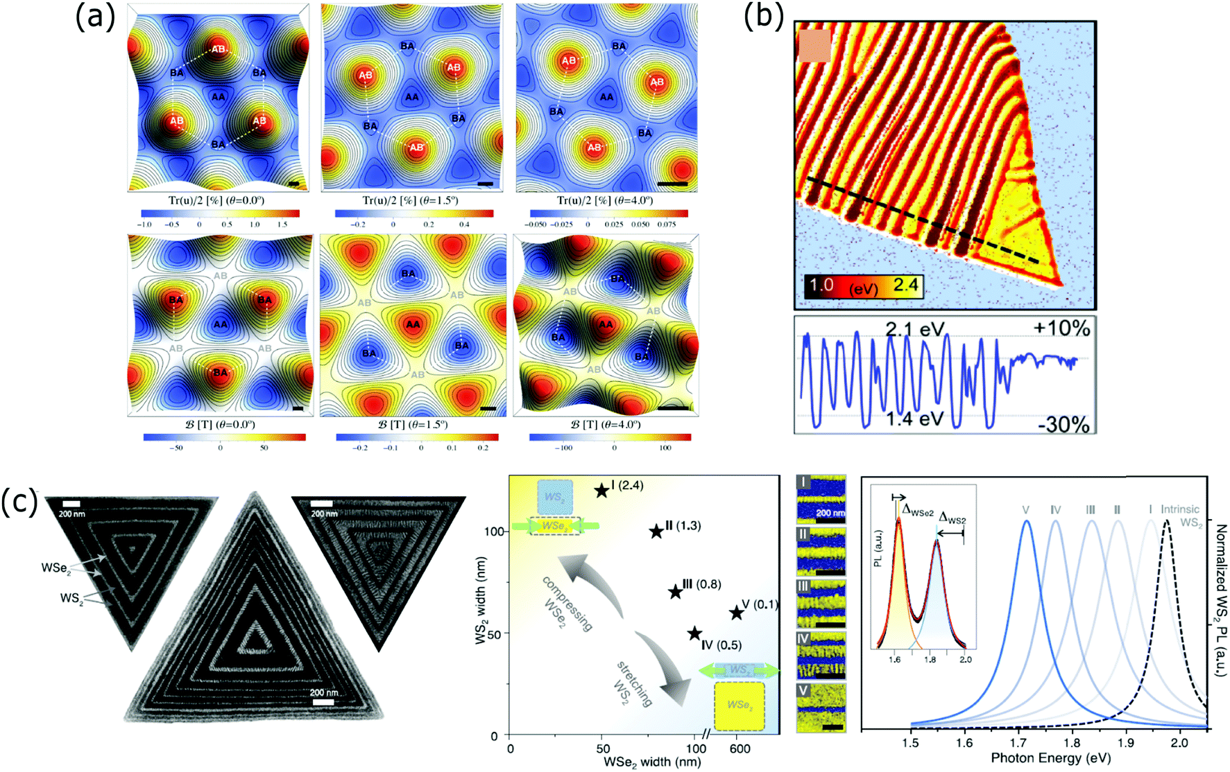 | ||
| Fig. 5 (a) Relative local expansion Tru/2 simulated in real space for twist angles of 0°, 1.5° and 4°. These mappings represent the level of straining as a function of the rotation angle (top). Pseudomagnetic field distribution simulated in real space for the same twist angles of 0°, 1.5° and 4°. These mappings represent the fields that originate as a result of the level of straining (bottom). Reproduced with permission from ref. 109. (b) Iso-absorption map representing the energy at which the squared absorption coefficient is equivalent to 7.5 × 10⁻¹¹ cm−2 at each point (top). A cross section along the dashed black line is shown at the bottom. The images show the existence of spatially variable absorption spectra following the periodic compressive and tensile strain regions in the BP ripples. Reproduced with permission from ref. 114. (c) SEM images of three different WS2/WSe2 superlattices fabricated from coherent epitaxial growth (left). Graph with the aspect ratios (values in parentheses) of the WS2/WSe2 widths at which the I to V superlattices were obtained and false-colour SEM images of the I–V superlattices (middle). Normalized PL spectra of the I–V superlattices together with the peak corresponding to the intrinsic WS2 to show the shift in wavelength (right). The inset spectrum of a typical WS2/WSe2 superlattice is represented to illustrate the relative WS2 peak red-shift and the relative WSe2 peak blue-shift. Reproduced with permission from ref. 115. | ||
Tuning the bandgap of semiconducting 2D materials is one of the main aims of strain engineering, relevant for optoelectronic applications. The formation of periodic ripples on a black phosphorus thin layer gave rise to an absorption spectrum with periodic absorption edge shifts of +10% and −30%, corresponding to the regions under tensile and compressive strains.125 An iso-absorption map shown in Fig. 5(b) illustrates the spatially varying optical properties induced by the periodic ripples of the black phosphorus flake. Coherent, full-matching lattice constants in-plane WS2/WSe2 superlattices were fabricated by metal–organic chemical vapor deposition. SEM images of three different superlattices are shown in Fig. 5(c) (left). The lattice coherence has been achieved by tensile (compressive) strain in the WS2 (WSe2) components. The ratio of their widths allows controlling the degree of strain, producing different types of superlattices (labelled as I to V within the panel) (Fig. 5(c), middle). Each type of superlattice (I to V) presents a red- (blue-) shifted peak in the photoluminescence spectra with respect to the intrinsic WS2 (WSe2). The spectrum is shown in Fig. 5(c) (right) and demonstrates the potential to use this approach for tunable optoelectronic devices.126 The misfit dislocations formed at the interface of a lateral WSe2/WS2 heterostructure as a result of the lattice mismatch between both layers were used as templates to grow WS2 sub-2 nm quantum wells on a WSe2 matrix superlattice by chemical vapour deposition. The strain field surrounding the misfit dislocations was found to induce dislocation climb by the preferential growth of the quantum wells.127
Rigorously, strain is the mechanism that is common in almost all types of superlattices described in this Feature article through the lattice mismatch or the stress induced on the 2D material layers when they are stacked together or placed in a patterned topography. For this reason, a deep study and understanding of its influence on the fabrication of superlattices in particular, and any other device in general, will be fundamental for the advance of the 2D materials field.
2.5 Lithographic-engineered superlattices
This section includes those works where the periodicity of the superlattice was created by either transferring a 2D material onto a substrate with an ordered array of structures that served as templates to tailor its electronic and optical properties or by patterning selectively a 2D material layer by a lithographic method.The top panel of Fig. 6(a) shows a schematic of a MoS2 monolayer transferred onto an array of periodic SiO2 nanocones, which are assembled by nanosphere lithography. At the apex of the nanocones, the more stretched areas of MoS2 present a high tensile strain, which results in a periodic decrease in its optical bandgap. Therefore, a large area artificial-atom crystal is produced. Raman and photoluminescence measurements showed that the crystal presented a large exciton binding energy. Fig. 6(a) (bottom left) shows a scanning PL map of the artificial crystal. Under illumination with wavelength larger than the bandgap of MoS2, excitons are created in MoS2. These excitons drift towards the nanocone tips and then are emitted with a larger wavelength. A scheme of the process is shown in Fig. 6(a) (bottom right).128 Another group employed an alternative approach to fabricate artificial superlattices based on a MoS2 monolayer. They generated a periodic array of quantum dots inducing local phase change from 2H (semiconducting) to 1T (metallic) by focused electron beam exposure. By controlling the size and the pitch of the quantum dots, the tuning of the bandgap from 1.81 to 1.42 eV was demonstrated.129 An artificial superlattice was achieved by transferring a graphene layer onto a self-assembled array of silicon oxide nanoparticles. The quasi-periodic strain produced on graphene gave rise to minibands with broad density of states. The authors claimed that this result constituted a cheap and simple process to fabricate superlattices for optical modulators or infrared sensors.130 In another work, a graphene layer was transferred onto an array of gold nanoislands. Thermal annealing creates a hybrid graphene/gold superstructure where the stretching of graphene and the phase change in gold gave rise to unusually large moiré periodicities.131
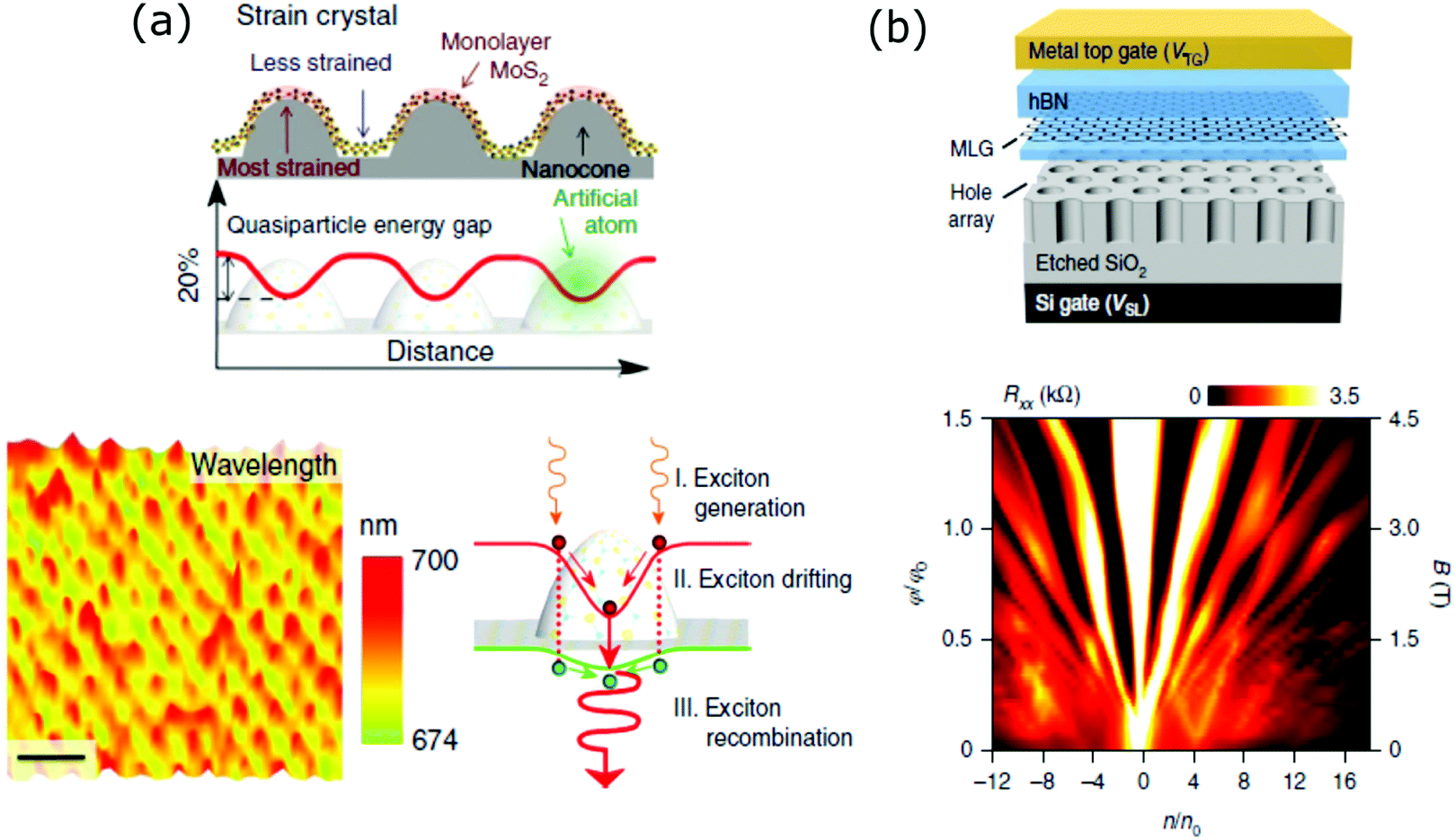 | ||
| Fig. 6 (a) Scheme of the artificial-atom crystal by transferring of the MoS2 monolayer on an array of periodic SiO2 nanocones. The energy bandgap reduction is inverse of the strain level (top). Scanning PL spectroscopy mapping of the artificial crystal (bottom left). Scheme of the process that the excitons undergo once they are induced on the artificial crystal under light exposure (bottom right). Reproduced with permission from ref. 117. (b) Scheme of a final device consisting of a fully encapsulated graphene structure transferred onto a patterned dielectric superlattice (top). Device Rxx resistance measured as a function of normalized density and magnetic field. A Hofstadter butterfly behaviour is achieved. Conditions: Vsuperlattice = 50 V, T = 250 mK, application of a triangular periodic potential (bottom). Reproduced with permission from ref. 122. | ||
The previous section showed the results where moiré patterning was employed to tune the bandgap structure of graphene. A second route to achieve this is by nanostructuring the material by lithographic methods. In a recent work, an array of triangular shaped holes with a pitch of 35 nm and minimum feature sizes of 12–15 nm was defined on a h-BN/graphene/h-BN heterostructure by electron beam lithography. The small size and the high density of the holes were chosen to manipulate the electronic and magnetic quantum transport behaviour.132 A third route to engineer the electronic properties of graphene is by applying external electric fields rather than modifying the material itself. A fully encapsulated h-BN/graphene/h-BN heterostructure was transferred onto a 300 nm SiO2 substrate with an array of periodic nanoholes defined by electron beam lithography. A scheme of the device is shown in Fig. 6(b), top. This patterned dielectric layer was the component that induced a superlattice structure on graphene, by introducing periodic potentials with triangular or square unit cells. As a result, Dirac cones and Hofstadter butterfly behaviours were replicated from non-moiré generated superlattices. Fig. 6(b) (bottom) shows a Hofstadter's butterfly spectrum achieved at 4.5 T, while the observation of the Hofstadter spectrum from moiré superlattices requires magnetic fields higher than 20 T up to now.133
Lithography is ubiquitous in the fabrication of devices. However, in the case of 2D material based superlattices, the results from the examples shown in this section can be obtained by using one of the methods described in the previous sections. This poses the question whether the lithographic-engineered approach is well-suited to produce optimal van der Waals based superlattices in comparison with the other strategies, since the mixed dimensionality of a 2D material flake and the 3D pattern substrate can introduce an additional complexity to the interlayer interaction and expensive and complex techniques such as electron and focused ion beam are required to define high-resolution periodic potentials on a 2D material surface.
3 Conclusion and outlook
2D materials and their van der Waals interlayer interaction display physical and chemical properties unobserved in their bulk counterparts. This unique trait has opened the way to produce devices with novel architectures, among which the fabrication of van der Waals 2D material superlattices has been explored. Our aim in the present Feature article was to underscore the huge potential and relevance of this type of structures, which comprise a very young field yet. The first prototypes have shown improved thermoelectric, optoelectronic, phase-change memory and energy storage performances, compared to the devices fabricated with established methods. These achievements constitute an invitation to explore the two-dimensional material based superlattices for solving environmental and energy consumption related issues. Particularly, they could have a great impact on the thermoelectrical and Li-/Na-storage applications. At the fundamental level, the moiré superlattices have displayed novel electronic, excitonic, superconductive, and magnetic states. The field of twistronics has just started and a plethora of new physical phenomena is expected in the future. Strain is present in almost all types of superlattices, both introduced unintentionally or as a variable to modulate their properties. Therefore, a rigorous study of the influence of strain or strain engineering on the final properties of the structures will be fundamental for the controlled fabrication of high-quality superlattices. The superlattices based on van der Waals 2D materials have shown huge versatility. As an example, the bandgap can be modulated by the composition of the superlattice unit cell, controlling the interlayer interaction, intercalating ions or molecules at the interlayer, moiré patterning, strain engineering, and combining 2D materials with conventional lithographic approaches. This illustrates the potential to design and devise superlattices. For the same reason, many research groups from different chemical and physical backgrounds can have access to their fabrication. Finally, the improvement and expansion of the robotic assembly approach will be crucial for the viability of 2D material based superlattices at both the academic and industrial level. At the academic level, automation would allow the researchers to save time and increase the success yield in the fabrication of complex superlattices, in order to focus on the study and engineering of their properties. The robotic assembly has room to introduce more variables such as the twist angle, the doping level or the cleaning of the flakes, which will result in the production of high-quality superlattices. At the industrial level, the remaining challenge is the implementation of large-scale manufacturing of these superlattices.Conflicts of interest
There are no conflicts to declare.Acknowledgements
This project has received funding from the European Research Council (ERC) under European Union's Horizon 2020 research and innovation programme (grant agreement no 755655, ERC-StG 2017 project 2D-TOPSENSE). R. F. acknowledges the support from the Spanish Ministry of Economy, Industry and Competitiveness through a Juan de la Cierva-formación fellowship 2017 FJCI-2017-32919. We acknowledge support of the publication fee by the CSIC Open Access Publication Support Initiative through its Unit of Information Resources for Research (URICI).References
- L. Esaki and R. Tsu, IBM J. Res. Dev., 1970, 14, 61–65 CAS.
- L. Esaki and L. L. Chang, Phys. Rev. Lett., 1974, 33, 495–498 CrossRef CAS.
- G. C. Osbourn, IEEE J. Quantum Electron., 1986, 22, 1677–1681 CrossRef.
- H. T. Grahn, Semiconductor superlattices: growth and electronic properties, World Scientific, 1995 Search PubMed.
- R. Tsu, Superlattice to nanoelectronics, Elsevier, 2010 Search PubMed.
- E. E. Mendez and K. von Klitzing, Physics and applications of quantum wells and superlattices, Springer Science & Business Media, 2012, vol. 170 Search PubMed.
- C. M. Lieber, Nano Lett., 2002, 2, 81–82 CrossRef CAS.
- M. Hu and D. Poulikakos, Nano Lett., 2012, 12, 5487–5494 CrossRef CAS PubMed.
- M. Hocevar, G. Immink, M. Verheijen, N. Akopian, V. Zwiller, L. Kouwenhoven and E. Bakkers, Nat. Commun., 2012, 3, 1–6 Search PubMed.
- J. K. Hyun, S. Zhang and L. J. Lauhon, Annu. Rev. Mater. Res., 2013, 43, 451–479 CrossRef CAS.
- M. Zhao, Y. Wang, Q. Ma, Y. Huang, X. Zhang, J. Ping, Z. Zhang, Q. Lu, Y. Yu, H. Xu, Y. Zhao and H. Zhang, Adv. Mater., 2015, 27, 7372–7378 CrossRef CAS PubMed.
- Y. Dou, L. Zhang, J. Xu, C. T. He, X. Xu, Z. Sun, T. Liao, B. Nagy, P. Liu and S. X. Dou, ACS Nano, 2018, 12, 1878–1886 CrossRef CAS PubMed.
- S. Gu, S. Wu, L. Cao, M. Li, N. Qin, J. Zhu, Z. Wang, Y. Li, Z. Li, J. Chen and Z. Lu, J. Am. Chem. Soc., 2019, 141, 9623–9628 CrossRef CAS PubMed.
- S. Wang, Q. Wang, P. Shao, Y. Han, X. Gao, L. Ma, S. Yuan, X. Ma, J. Zhou, X. Feng and B. Wang, J. Am. Chem. Soc., 2017, 139, 4258–4261 CrossRef CAS PubMed.
- A. J. Molina-Mendoza, E. Giovanelli, W. S. Paz, M. A. Niño, J. O. Island, C. Evangeli, L. Aballe, M. Foerster, H. S. J. Van Der Zant and G. Rubio-Bollinger, et al. , Nat. Commun., 2017, 8, 14409 CrossRef CAS PubMed.
- M. Velický, P. S. Toth, A. M. Rakowski, A. P. Rooney, A. Kozikov, C. R. Woods, A. Mishchenko, L. Fumagalli, J. Yin, V. Zólyomi, T. Georgiou, S. J. Haigh, K. S. Novoselov and R. A. W. Dryfe, Nat. Commun., 2017, 8, 14410 CrossRef PubMed.
- K. Ray, A. E. Yore, T. Mou, S. Jha, K. K. H. Smithe, B. Wang, E. Pop and A. K. M. Newaz, ACS Nano, 2017, 11(6), 6024–6030 CrossRef CAS PubMed.
- G. Prando, Nat. Nanotechnol., 2017, 12, 191 CrossRef CAS PubMed.
- R. Gusmão, Z. Sofer, J. Luxa and M. Pumera, J. Mater. Chem. A, 2018, 6(34), 16590–16599 RSC.
- Y. Niu, J. Villalva, R. Frisenda, G. Sanchez-Santolino, L. Ruiz-González, E. M. Pérez, M. García-Hernández, E. Burzurí and A. Castellanos-Gomez, 2D Mater., 2019, 6, 035023 CrossRef.
- G. H. Moh, Mineral. Petrol., 1987, 36, 191–204 CrossRef CAS.
- K. Kang, K.-H. Lee, Y. Han, H. Gao, S. Xie, D. A. Muller and J. Park, Nature, 2017, 550, 229 CrossRef PubMed.
- S. Masubuchi, M. Morimoto, S. Morikawa, M. Onodera, Y. Asakawa, K. Watanabe, T. Taniguchi and T. Machida, Nat. Commun., 2018, 9, 1413 CrossRef PubMed.
- S. Vishwanath, X. Liu, S. Rouvimov, L. Basile, N. Lu, A. Azcatl, K. Magno, R. M. Wallace, M. Kim and J.-C. Idrobo, et al. , J. Mater. Res., 2016, 31, 900–910 CrossRef CAS.
- A. Koma, Thin Solid Films, 1992, 216, 72–76 CrossRef CAS.
- M. Lin, D. Wu, Y. Zhou, W. Huang, W. Jiang, W. Zheng, S. Zhao, C. Jin, Y. Guo and H. Peng, et al. , J. Am. Chem. Soc., 2013, 135, 13274–13277 CrossRef CAS PubMed.
- Y. Zhao, H. Liu, X. Guo, Y. Jiang, Y. Sun, H. Wang, Y. Wang, H.-D. Li, M.-H. Xie and X.-C. Xie, et al. , Nano Lett., 2014, 14, 5244–5249 CrossRef CAS PubMed.
- X.-B. Li, N.-K. Chen, X.-P. Wang and H.-B. Sun, Adv. Funct. Mater., 2018, 28, 1803380 CrossRef.
- J. Momand, R. Wang, J. E. Boschker, M. A. Verheijen, R. Calarco and B. J. Kooi, Nanoscale, 2015, 7, 19136–19143 RSC.
- S. Cecchi, E. Zallo, J. Momand, R. Wang, B. J. Kooi, M. A. Verheijen and R. Calarco, APL Mater., 2017, 5, 26107 CrossRef.
- A. V. Kolobov, P. Fons, Y. Saito and J. Tominaga, ACS Omega, 2017, 2, 6223–6232 CrossRef CAS PubMed.
- J. Tominaga, Y. Saito, K. Mitrofanov, N. Inoue, P. Fons, A. V. Kolobov, H. Nakamura and N. Miyata, Adv. Funct. Mater., 2017, 27, 1702243 CrossRef.
- J. K. Behera, X. Zhou, A. Ranjan and R. E. Simpson, ACS Appl. Mater. Interfaces, 2018, 10, 15040–15050 CrossRef CAS PubMed.
- R. Mondal, Y. Aihara, Y. Saito, P. Fons, A. V. Kolobov, J. Tominaga and M. Hase, ACS Appl. Mater. Interfaces, 2018, 10, 26781–26786 CrossRef CAS PubMed.
- M. Falmbigl, M. B. Alemayehu, D. R. Merrill, M. Beekman and D. C. Johnson, Cryst. Res. Technol., 2015, 50, 464–472 CrossRef CAS.
- D. Merrill, D. Moore, S. Bauers, M. Falmbigl and D. Johnson, Materials, 2015, 8, 2000–2029 CrossRef CAS PubMed.
- M. Beekman, C. L. Heideman and D. C. Johnson, Semicond. Sci. Technol., 2014, 29, 64012 CrossRef.
- R. D. Westover, J. Ditto, M. Falmbigl, Z. L. Hay and D. C. Johnson, Chem. Mater., 2015, 27, 6411–6417 CrossRef CAS.
- R. Atkins, J. Wilson, P. Zschack, C. Grosse, W. Neumann and D. C. Johnson, Chem. Mater., 2012, 24, 4594–4599 CrossRef CAS.
- G. Mitchson, E. Hadland, F. Göhler, M. Wanke, M. Esters, J. Ditto, E. Bigwood, K. Ta, R. G. Hennig and T. Seyller, et al. , ACS Nano, 2016, 10, 9489–9499 CrossRef CAS PubMed.
- D. M. Hamann, A. C. Lygo, M. Esters, D. R. Merrill, J. Ditto, D. R. Sutherland, S. R. Bauers and D. C. Johnson, ACS Nano, 2018, 12, 1285–1295 CrossRef CAS PubMed.
- M. B. Alemayehu, K. Ta, M. Falmbigl and D. C. Johnson, Nanoscale, 2015, 7, 7378–7385 RSC.
- F. Göhler, G. Mitchson, M. B. Alemayehu, F. Speck, M. Wanke, D. C. Johnson and T. Seyller, J. Phys.: Condens. Matter, 2018, 30, 55001 CrossRef PubMed.
- M. Falmbigl, A. Fiedler, R. E. Atkins, S. F. Fischer and D. C. Johnson, Nano Lett., 2015, 15, 943–948 CrossRef CAS PubMed.
- D. R. Merrill, D. R. Sutherland, J. Ditto, S. R. Bauers, M. Falmbigl, D. L. Medlin and D. C. Johnson, Chem. Mater., 2015, 27, 4066–4072 CrossRef CAS.
- S. R. Wood, D. R. Merrill, G. Mitchson, A. C. Lygo, S. R. Bauers, D. M. Hamann, D. R. Sutherland, J. Ditto and D. C. Johnson, Chem. Mater., 2016, 29, 773–779 CrossRef.
- C. Yin, Q. Hu, G. Wang, T. Huang, X. Zhou, X. Zhang, Y. Dou, B. Kang, J. Tang and N. Liu, et al. , Appl. Phys. Lett., 2017, 110, 43507 CrossRef.
- P. Jood, M. Ohta, H. Nishiate, A. Yamamoto, O. I. Lebedev, D. Berthebaud, K. Suekuni and M. Kunii, Chem. Mater., 2014, 26, 2684–2692 CrossRef CAS.
- R. Guo, Y.-D. Jho and A. J. Minnich, Nanoscale, 2018, 10, 14432–14440 RSC.
- Z. Li, S. R. Bauers, N. Poudel, D. Hamann, X. Wang, D. S. Choi, K. Esfarjani, L. Shi, D. C. Johnson and S. B. Cronin, Nano Lett., 2017, 17, 1978–1986 CrossRef CAS PubMed.
- H. Bai, X. Yang, Y. Liu, M. Zhang, M. Wang, Y. Li, J. Ma, Q. Tao, Y. Xie and G.-H. Cao, et al. , J. Phys.: Condens. Matter, 2018, 30, 355701 CrossRef PubMed.
- R. Sankar, G. Peramaiyan, I. Panneer Muthuselvam, C.-Y. Wen, X. Xu and F. C. Chou, Chem. Mater., 2018, 30, 1373–1378 CrossRef CAS.
- C. Grosse, M. B. Alemayehu, M. Falmbigl, A. Mogilatenko, O. Chiatti, D. C. Johnson and S. F. Fischer, Sci. Rep., 2016, 6, 33457 CrossRef CAS PubMed.
- M. Trahms, C. Grosse, M. B. Alemayehu, O. K. Hite, O. Chiatti, A. Mogilatenko, D. C. Johnson and S. F. Fischer, Supercond. Sci. Technol., 2018, 31, 65006 CrossRef.
- J. Yao, K. J. Koski, W. Luo, J. J. Cha, L. Hu, D. Kong, V. K. Narasimhan, K. Huo and Y. Cui, Nat. Commun., 2014, 5, 5670 CrossRef CAS PubMed.
- Y. Guo, J. Zhou, Y. Liu, X. Zhou, F. Yao, C. Tan, J. Wu, L. Lin, K. Liu and Z. Liu, et al. , Adv. Mater., 2017, 29, 1703424 CrossRef PubMed.
- D. K. Bediako, M. Rezaee, H. Yoo, D. T. Larson, S. Y. F. Zhao, T. Taniguchi, K. Watanabe, T. L. Brower-Thomas, E. Kaxiras and P. Kim, Nature, 2018, 558, 425 CrossRef CAS PubMed.
- Q. Liu, X. Li, Z. Xiao, Y. Zhou, H. Chen, A. Khalil, T. Xiang, J. Xu, W. Chu and X. Wu, et al. , Adv. Mater., 2015, 27, 4837–4844 CrossRef CAS PubMed.
- E. Hitz, J. Wan, A. Patel, Y. Xu, L. Meshi, J. Dai, Y. Chen, A. Lu, A. V. Davydov and L. Hu, ACS Appl. Mater. Interfaces, 2016, 8, 11390–11395 CrossRef CAS PubMed.
- C. Wang, Q. He, U. Halim, Y. Liu, E. Zhu, Z. Lin, H. Xiao, X. Duan, Z. Feng and R. Cheng, et al. , Nature, 2018, 555, 231 CrossRef CAS PubMed.
- G. E. Wang, G. Xu, N. Zhang, M. S. Yao, M. S. Wang and G. C. Guo, Angew. Chem., 2019, 131(9), 2718–2721 CrossRef.
- Z. Li, Y. Zhao, K. Mu, H. Shan, Y. Guo, J. Wu, Y. Su, Q. Wu, Z. Sun and A. Zhao, et al. , J. Am. Chem. Soc., 2017, 139, 16398–16404 CrossRef CAS PubMed.
- C. Wan, Y. Kodama, M. Kondo, R. Sasai, X. Qian, X. Gu, K. Koga, K. Yabuki, R. Yang and K. Koumoto, Nano Lett., 2015, 15, 6302–6308 CrossRef CAS PubMed.
- C. Wan, X. Gu, F. Dang, T. Itoh, Y. Wang, H. Sasaki, M. Kondo, K. Koga, K. Yabuki and G. J. Snyder, et al. , Nat. Mater., 2015, 14, 622 CrossRef CAS PubMed.
- C. Wan, R. Tian, M. Kondou, R. Yang, P. Zong and K. Koumoto, Nat. Commun., 2017, 8, 1024 CrossRef PubMed.
- J. Xu, J. Zhang, W. Zhang and C.-S. Lee, Adv. Energy Mater., 2017, 7, 1700571 CrossRef.
- C. Zhao, X. Wang, J. Kong, J. M. Ang, P. S. Lee, Z. Liu and X. Lu, ACS Appl. Mater. Interfaces, 2016, 8, 2372–2379 CrossRef CAS PubMed.
- P. Xiong, R. Ma, N. Sakai, L. Nurdiwijayanto and T. Sasaki, ACS Energy Lett., 2018, 3, 997–1005 CrossRef CAS.
- P. Xiong, R. Ma, N. Sakai and T. Sasaki, ACS Nano, 2018, 12, 1768–1777 CrossRef CAS PubMed.
- P. Xiong, X. Zhang, F. Zhang, D. Yi, J. Zhang, B. Sun, H. Tian, D. Shanmukaraj, T. Rojo and M. Armand, et al. , ACS Nano, 2018, 12, 12337–12346 CrossRef CAS PubMed.
- M. S. Islam, M. Kim, X. Jin, S. M. Oh, N.-S. Lee, H. Kim and S.-J. Hwang, ACS Energy Lett., 2018, 3, 952–960 CrossRef CAS.
- S. Kumar, J. Jagielski, S. Yakunin, P. Rice, Y.-C. Chiu, M. Wang, G. Nedelcu, Y. Kim, S. Lin and E. J. G. Santos, et al. , ACS Nano, 2016, 10, 9720–9729 CrossRef CAS PubMed.
- J. Zhou, Y. Chu and J. Huang, ACS Appl. Mater. Interfaces, 2016, 8, 25660–25666 CrossRef CAS PubMed.
- J.-C. Blancon, H. Tsai, W. Nie, C. C. Stoumpos, L. Pedesseau, C. Katan, M. Kepenekian, C. M. M. Soe, K. Appavoo and M. Y. Sfeir, et al. , Science, 2017, 355, 1288–1292 CrossRef CAS PubMed.
- L. Dou, A. B. Wong, Y. Yu, M. Lai, N. Kornienko, S. W. Eaton, A. Fu, C. G. Bischak, J. Ma and T. Ding, et al. , Science, 2015, 349, 1518–1521 CrossRef CAS PubMed.
- P. Guo, C. C. Stoumpos, L. Mao, S. Sadasivam, J. B. Ketterson, P. Darancet, M. G. Kanatzidis and R. D. Schaller, Nat. Commun., 2018, 9, 2019 CrossRef PubMed.
- B. Cheng, T.-Y. Li, P.-C. Wei, J. Yin, K.-T. Ho, J. R. D. Retamal, O. F. Mohammed and J.-H. He, Nat. Commun., 2018, 9, 5196 CrossRef PubMed.
- H. Schmidt, J. C. Rode, D. Smirnov and R. J. Haug, Nat. Commun., 2014, 5, 5742 CrossRef PubMed.
- K. Schouteden, Z. Li, T. Chen, F. Song, B. Partoens, C. Van Haesendonck and K. Park, Sci. Rep., 2016, 6, 20278 CrossRef CAS PubMed.
- D. Wang, G. Chen, C. Li, M. Cheng, W. Yang, S. Wu, G. Xie, J. Zhang, J. Zhao and X. Lu, et al. , Phys. Rev. Lett., 2016, 116, 126101 CrossRef PubMed.
- S. Xu, Y. Han, X. Chen, Z. Wu, L. Wang, T. Han, W. Ye, H. Lu, G. Long and Y. Wu, et al. , Nano Lett., 2015, 15, 2645–2651 CrossRef CAS PubMed.
- X. Li, M.-W. Lin, J. Lin, B. Huang, A. A. Puretzky, C. Ma, K. Wang, W. Zhou, S. T. Pantelides and M. Chi, et al. , Sci. Adv., 2016, 2, e1501882 CrossRef PubMed.
- C. Zhang, C.-P. Chuu, X. Ren, M.-Y. Li, L.-J. Li, C. Jin, M.-Y. Chou and C.-K. Shih, Sci. Adv., 2017, 3, e1601459 CrossRef PubMed.
- T. Yang, B. Zheng, Z. Wang, T. Xu, C. Pan, J. Zou, X. Zhang, Z. Qi, H. Liu and Y. Feng, et al. , Nat. Commun., 2017, 8, 1906 CrossRef PubMed.
- L. Wang, S. Zihlmann, M.-H. Liu, P. Makk, K. Watanabe, T. Taniguchi, A. Baumgartner and C. Schönenberger, Nano Lett., 2019, 19(4), 2371–2376 CrossRef CAS PubMed.
- M. Yankowitz, Q. Ma, P. Jarillo-Herrero and B. J. LeRoy, Nat. Rev. Phys., 2019, 1 Search PubMed.
- M. Yankowitz, J. Xue, D. Cormode, J. D. Sanchez-Yamagishi, K. Watanabe, T. Taniguchi, P. Jarillo-Herrero, P. Jacquod and B. J. LeRoy, Nat. Phys., 2012, 8, 382 Search PubMed.
- D. R. Hofstadter, Phys. Rev. B: Condens. Matter Mater. Phys., 1976, 14, 2239 CrossRef CAS.
- C. R. Dean, L. Wang, P. Maher, C. Forsythe, F. Ghahari, Y. Gao, J. Katoch, M. Ishigami, P. Moon and M. Koshino, et al. , Nature, 2013, 497, 598 CrossRef CAS PubMed.
- B. Hunt, J. D. Sanchez-Yamagishi, A. F. Young, M. Yankowitz, B. J. LeRoy, K. Watanabe, T. Taniguchi, P. Moon, M. Koshino and P. Jarillo-Herrero, et al. , Science, 2013, 340, 1427–1430 CrossRef CAS PubMed.
- L. A. Ponomarenko, R. V. Gorbachev, G. L. Yu, D. C. Elias, R. Jalil, A. A. Patel, A. Mishchenko, A. S. Mayorov, C. R. Woods and J. R. Wallbank, et al. , Nature, 2013, 497, 594 CrossRef CAS PubMed.
- L. Wang, Y. Gao, B. Wen, Z. Han, T. Taniguchi, K. Watanabe, M. Koshino, J. Hone and C. R. Dean, Science, 2015, 350, 1231–1234 CrossRef CAS PubMed.
- R. K. Kumar, X. Chen, G. H. Auton, A. Mishchenko, D. A. Bandurin, S. V. Morozov, Y. Cao, E. Khestanova, M. Ben Shalom and A. V. Kretinin, et al. , Science, 2017, 357, 181–184 CrossRef PubMed.
- R. K. Kumar, A. Mishchenko, X. Chen, S. Pezzini, G. H. Auton, L. A. Ponomarenko, U. Zeitler, L. Eaves, V. I. Fal’ko and A. K. Geim, Proc. Natl. Acad. Sci. U. S. A., 2018, 115, 5135–5139 CrossRef CAS PubMed.
- C. R. Woods, L. Britnell, A. Eckmann, R. S. Ma, J. C. Lu, H. M. Guo, X. Lin, G. L. Yu, Y. Cao and R. V. Gorbachev, et al. , Nat. Phys., 2014, 10, 451 Search PubMed.
- J. C. W. Song, P. Samutpraphoot and L. S. Levitov, Proc. Natl. Acad. Sci. U. S. A., 2015, 112, 10879–10883 CrossRef CAS PubMed.
- G. Chen, L. Jiang, S. Wu, B. Lyu, H. Li, B. L. Chittari, K. Watanabe, T. Taniguchi, Z. Shi and J. Jung, et al. , Nat. Phys., 2019, 1 Search PubMed.
- G. X. Ni, H. Wang, J. S. Wu, Z. Fei, M. D. Goldflam, F. Keilmann, B. Özyilmaz, A. H. C. Neto, X. M. Xie and M. M. Fogler, et al. , Nat. Mater., 2015, 14, 1217 CrossRef CAS PubMed.
- H. Kim, N. Leconte, B. L. Chittari, K. Watanabe, T. Taniguchi, A. H. MacDonald, J. Jung and S. Jung, Nano Lett., 2018, 18, 7732–7741 CrossRef CAS PubMed.
- R. Bistritzer and A. H. MacDonald, Proc. Natl. Acad. Sci. U. S. A., 2011, 108, 12233–12237 CrossRef CAS PubMed.
- Y. Cao, V. Fatemi, S. Fang, K. Watanabe, T. Taniguchi, E. Kaxiras and P. Jarillo-Herrero, Nature, 2018, 556, 43 CrossRef CAS PubMed.
- J. C. W. Song and N. M. Gabor, Nat. Nanotechnol., 2018, 13, 986 CrossRef CAS PubMed.
- D. H. Freedman, Quanta Mag., 2019, https://www.quantamagazine.org/how-twisted-graphene-became-the-big-thing-in-physics-20190430/ Search PubMed.
- X. Lu, P. Stepanov, W. Yang, M. Xie, M. A. Aamir, I. Das, C. Urgell, K. Watanabe, T. Taniguchi and G. Zhang, et al., arXiv Prepr. arXiv1903.06513.
- S. S. Sunku, G. Ni, B.-Y. Jiang, H. Yoo, A. Sternbach, A. S. McLeod, T. Stauber, L. Xiong, T. Taniguchi and K. Watanabe, et al. , Science, 2018, 362, 1153–1156 CrossRef CAS PubMed.
- H. Yoo, R. Engelke, S. Carr, S. Fang, K. Zhang, P. Cazeaux, S. H. Sung, R. Hovden, A. W. Tsen, T. Taniguchi, K. Watanabe, G. C. Yi, M. Kim, M. Luskin, E. B. Tadmor, E. Kaxiras and P. Kim, Nat. Mater., 2019, 18, 448–453 CrossRef CAS PubMed.
- N. Zhang, A. Surrente, M. Baranowski, D. K. Maude, P. Gant, A. Castellanos-Gomez and P. Plochocka, Nano Lett., 2018, 18, 7651–7657 CrossRef CAS PubMed.
- C. Jin, E. C. Regan, A. Yan, M. Iqbal Bakti Utama, D. Wang, S. Zhao, Y. Qin, S. Yang, Z. Zheng, S. Shi, K. Watanabe, T. Taniguchi, S. Tongay, A. Zettl and F. Wang, Nature, 2019, 567, 76–80 CrossRef CAS PubMed.
- K. Tran, G. Moody, F. Wu, X. Lu, J. Choi, K. Kim, A. Rai, D. A. Sanchez, J. Quan and A. Singh, et al. , Nature, 2019, 1 Search PubMed.
- M. Yankowitz, K. Watanabe, T. Taniguchi, P. San-Jose and B. J. LeRoy, Nat. Commun., 2016, 7, 13168 CrossRef CAS PubMed.
- P. Kumar, J. Liu, M. Motlag, L. Tong, Y. Hu, X. Huang, A. Bandopadhyay, S. K. Pati, L. Ye and J. Irudayaraj, et al. , Nano Lett., 2018, 19, 283–291 CrossRef PubMed.
- Q. Tong, H. Yu, Q. Zhu, Y. Wang, X. Xu and W. Yao, Nat. Phys., 2017, 13, 356 Search PubMed.
- R. Roldán, A. Castellanos-Gomez, E. Cappelluti and F. Guinea, J. Phys.: Condens. Matter, 2015, 27, 313201 CrossRef PubMed.
- B. Amorim, A. Cortijo, F. de Juan, A. G. Grushin, F. Guinea, A. Gutiérrez-Rubio, H. Ochoa, V. Parente, R. Roldán, P. San-Jose, J. Schiefele, M. Sturla and M. A. H. Vozmediano, Phys. Rep., 2016, 617, 1–54 CrossRef CAS.
- Z. Lin, B. R. Carvalho, E. Kahn, R. Lv, R. Rao, H. Terrones, M. A. Pimenta and M. Terrones, 2D Mater., 2016, 3, 22002 CrossRef.
- Z. Dai, L. Liu and Z. Zhang, Adv. Mater., 2019, 1805417 CrossRef PubMed.
- X. Zhou, J. Kalikka, X. Ji, L. Wu, Z. Song and R. E. Simpson, Adv. Mater., 2016, 28, 3007–3016 CrossRef CAS PubMed.
- J. Kalikka, X. Zhou, E. Dilcher, S. Wall, J. Li and R. E. Simpson, Nat. Commun., 2016, 7, 11983 CrossRef CAS PubMed.
- J. Jung, A. M. DaSilva, A. H. MacDonald and S. Adam, Nat. Commun., 2015, 6, 6308 CrossRef CAS PubMed.
- P. San-Jose, A. Gutiérrez-Rubio, M. Sturla and F. Guinea, Phys. Rev. B: Condens. Matter Mater. Phys., 2014, 90, 75428 CrossRef.
- M. M. Van Wijk, A. Schuring, M. I. Katsnelson and A. Fasolino, Phys. Rev. Lett., 2014, 113, 135504 CrossRef CAS PubMed.
- F. Guinea, M. I. Katsnelson and A. K. Geim, Nat. Phys., 2010, 6, 30 Search PubMed.
- D. Nandwana and E. Ertekin, Nano Lett., 2015, 15, 1468–1475 CrossRef CAS PubMed.
- A. De Sanctis, J. D. Mehew, S. Alkhalifa, F. Withers, M. F. Craciun and S. Russo, Nano Lett., 2018, 18, 7919–7926 CrossRef CAS PubMed.
- J. Quereda, P. San-Jose, V. Parente, L. Vaquero-Garzon, A. J. Molina-Mendoza, N. Agrät, G. Rubio-Bollinger, F. Guinea, R. Roldán and A. Castellanos-Gomez, Nano Lett., 2016, 16, 2931–2937 CrossRef CAS PubMed.
- S. Xie, L. Tu, Y. Han, L. Huang, K. Kang, K. U. Lao, P. Poddar, C. Park, D. A. Muller and R. A. DiStasio, et al. , Science, 2018, 359, 1131–1136 CrossRef CAS PubMed.
- W. Zhou, Y.-Y. Zhang, J. Chen, D. Li, J. Zhou, Z. Liu, M. F. Chisholm, S. T. Pantelides and K. P. Loh, Sci. Adv., 2018, 4, eaap9096 CrossRef PubMed.
- H. Li, A. W. Contryman, X. Qian, S. M. Ardakani, Y. Gong, X. Wang, J. M. Weisse, C. H. Lee, J. Zhao and P. M. Ajayan, et al. , Nat. Commun., 2015, 6, 7381 CrossRef CAS PubMed.
- X. Xie, J. Kang, W. Cao, J. H. Chu, Y. Gong, P. M. Ajayan and K. Banerjee, Sci. Rep., 2017, 7, 9965 CrossRef PubMed.
- Y. Zhang, Y. Kim, M. J. Gilbert and N. Mason, npj 2D Mater. Appl., 2018, 2, 31 CrossRef.
- A. Pálinkás, P. Süle, M. Szendrő, G. Molnár, C. Hwang, L. P. Biró and Z. Osváth, Carbon N. Y., 2016, 107, 792–799 CrossRef.
- B. S. Jessen, L. Gammelgaard, M. R. Thomsen, D. M. A. Mackenzie, J. D. Thomsen, J. M. Caridad, E. Duegaard, K. Watanabe, T. Taniguchi and T. J. Booth, et al. , Nat. Nanotechnol., 2019, 1 Search PubMed.
- C. Forsythe, X. Zhou, K. Watanabe, T. Taniguchi, A. Pasupathy, P. Moon, M. Koshino, P. Kim and C. R. Dean, Nat. Nanotechnol., 2018, 13, 566 CrossRef CAS PubMed.
| This journal is © The Royal Society of Chemistry 2019 |