
 Open Access Article
 This Open Access Article is licensed under a
 Creative Commons Attribution 3.0 Unported Licence
High performance photoanodic catalyst prepared from an active organic photovoltaic cell – high potential gain from visible light†
Keiji
Nagai
 *a,
Takayuki
Kuwabara‡
b,
Mohd Fairus
Ahmad
ac,
Masahiro
Nakano
b,
Makoto
Karakawa
d,
Tetsuya
Taima
d and
Kohshin
Takahashi
*b
*a,
Takayuki
Kuwabara‡
b,
Mohd Fairus
Ahmad
ac,
Masahiro
Nakano
b,
Makoto
Karakawa
d,
Tetsuya
Taima
d and
Kohshin
Takahashi
*b
aLaboratory for Chemistry and Life Science, Institute of Innovative Research, Tokyo Institute of Technology, R1-26, Suzukake-dai, Midori-ku, Yokohama 226-8503, Kanagawa, Japan. E-mail: nagai.k.ae@m.titech.ac.jp
bGraduate School of Natural Science and Technology, Kanazawa University, Kakuma-machi, Kanazawa, Ishikawa 920-1192, Japan
cSchool of Microelectronic Engineering, Kampus Pauh, Universiti Malaysia Perlis, 02600, Arau, Perlis, Malaysia
dNanomaterial Research Institute, Kanazawa University, Kakuma-machi, Kanazawa, Ishikawa 920-1192, Japan
First published on 1st October 2019
Abstract
Photoelectrochemical oxidation of thiols was enhanced with a threshold potential of −0.35 V vs. Ag/AgCl by the use of a ZnPc/PCBM:P3HT/ZnO electode, which was prepared by removing the PEDOT:PSS/Au electrode of an inverted OPV device and coating it with ZnPc. A co-photocatalysis property of ZnPc was observed in the photoelectrochemistry and scanning Kelvin probe microscopy.
The organic photovoltaic (OPV) devices have potential in low-cost, large-area printing routes with high efficiency owing to the variety of organic materials.1 The active layer has a role to absorb photons and convert them to electrostatic energy in the form of separated electron and hole pairs. If the separated charge in its active layer can be utilized in chemical reactions directly without collection by electrodes, it would be a simple device for photoenergy conversion and have great merit to use the photon energy. From such a viewpoint, the research field of organic photoelectrochemical cells (OPECs)2–15 and organophotocatalysts14–19 has been refocused recently, while pioneer research started more than 30 years ago.20 A recent trend is metal or metal oxide coating on bulk heterojunction (BHJ) OPVs to construct OPECs and its efficiency enhancement,2–6 while the combination with rare metal is not so attractive for the choice of organic active layer. As an organic catalyst, phthalocyanine has a considerable activity and stablility. An alternative centering metal in phthalocyanine is also interesting to control its redox properties.13,21
In the conventional OPV devices, the active layer is sandwiched between a transparent electrode and an Al electrode as the back electrode. The so-called inverted-type OPVs have a noncorrosive Au metal as the back electrode and an ITO or a transparent front electrode.22–39 The inverted-type OPVs can be fabricated in ambient conditions and exhibit reasonable performance and stability especially with a stable n-type semiconductor, TiO2,22–32 ZnO33–38 or ZnS,39 as an electron collection layer.
For example, the ITO/amorphous TiOx/[6,6]-phenyl-C61-butyric acid methyl ester:regioregular poly(3-hexylthiophene)(PCBM:P3HT)/poly(3,4-ethylenediox-ylenethiophene):poly(4-styrenesulfonic acid) (PEDOT:PSS)/Au inverted-type cell (ITO/TiOx/PCBM:P3HT/PEDOT:PSS/Au) showed a power conversion efficiency (PCE) of 2.3% and the performance of the cells without sealing was about the same after continuous light irradiation for 100 h in an ambient atmosphere.31
In the present paper, the inverted-type OPV with ZnO was chosen as a precursor electrode to prepare a new photoanode to induce oxidation (Scheme 1). Experimental details are provided in the ESI.†
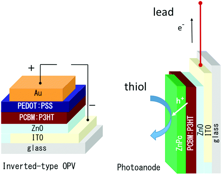 | ||
| Scheme 1 The structure of the inverted-type organic photovoltaic device (left) and photoanode prepared from it by removing the hole collecting electrode and covering it with co-photocatalyst ZnPc. | ||
The photovoltaic performance of the (ITO/ZnO/PCBM:P3HT/PEDOT:PSS/Au) was confirmed as shown in Fig. S1 (ESI†), and the PEDOT:PSS/Au hole collecting electrode was removed mechanically, because of weak adhesion between PCBM:P3HT and PEDOT:PSS,40 where almost complete removal of the PEDOT:PSS layer was observed. The inverted-type OPV devices have the same ordering of the layer structure as the photoanode on ITO, so the removal is a promising and repeatable technique to construct a well-characterized photoanode.
Fig. S2(a) (ESI†) is an FE-SEM image for the cross section of the BHJ electrode, and indicates ordered layer structure for glass/ITO/ZnO/PCBM:P3HT. From here we denote it as the BHJ electrode. The thickness values for ITO, ZnO, and PCBM:P3HT were estimated to be 185 nm, 50 nm, and 200 nm, respectively. As the top view in Fig. S2(b) (ESI†) shows, the sub 100 nm structure may be due to the roughness of the BHJ surface. Fig. S3 (ESI†) shows visible-near-infrared absorption spectra for the BHJ electrode, the ZnPc coated BHJ electrode, ZnPc and ITO. The BHJ active layers exhibited an identical one to that of the reported ones,38 and their absorption coefficients agreed with the thickness of the film. For the ZnPc coated BHJ electrode, slight increment from that without ZnPc was observed at >650 nm and was consistent with 8 nm coating of ZnPc.
Fig. 1 shows voltammograms in a thiol solution for the BHJ electrode (a) and the ZnPc coated BHJ electrode (b). The photoanodic current (red) for the electrode with ZnPc (b) was much larger than that without ZnPc (a). For the ZnPc coated BHJ electrode with ZnO, the threshold potential of the photoanodic current was around −0.35 V vs. Ag/AgCl. For the comparison with previous data without ZnO, a rapid scan of 20 mV s−1 is shown in Fig. S5b (ESI†), where a similar threshold potential (−0.38 V) to the slow scan (Fig. 1b) was observed. On the other hand, for the ZnPc coated BHJ electrode without ZnO, the threshold potential of the photoanodic current was around −0.0 V vs. Ag/AgCl as shown in our previous paper.18 The present larger gain than that without ZnO would be due to the effect of ZnO as a hole blocking layer. The threshold value of −0.35 V vs. Ag/AgCl was almost equal to the conduction band edge potential of ZnO (Fig. S6, ESI†), that is, the photogenerated electrons in the BHJ active layer can preferentially transfer to ZnO when the anodic polarization of ITO was deeper than the ZnO edge. The rapid scan data showed more photoanodic current (Fig. S5b, ESI†) than that for the slow scan (Fig. 1b). This means that the photoanodic performance of the photoanode is high as the diffusion limiting region of the thiol. Note that the ZnPc electrode exhibited an anodic current in the dark as shown in Fig. S7 (ESI†), that is, the ZnPc can function as a catalyst of 2-mercaptoethanol oxidation. The large anodic photocurrent may be caused by such a catalytic function of ZnPc.
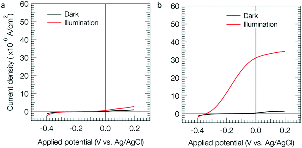 | ||
| Fig. 1 Linear sweep voltammograms for the BHJ (a) and ZnPc coated BHJ (b) electrodes. Concentration of thiol, 10 mM (pH = 11); light intensity, 70 mW cm−2 (Fig. S4, ESI†); scan rate, 0.5 mV s−1. | ||
Fig. 2 shows the action spectra of IPCE values (eqn (S1), ESI†) at a bias potential of +0.2 V vs. Ag/AgCl for the steady photocurrent. The action spectrum for the BHJ electrode (red circle) was consistent with the visible-near infrared absorption shown in Fig. S3 (ESI†). The IPCE was less than 1%, which was negligible in comparison to that in the OPV case to be almost 100% at the maximum absorbance wavelength.1 For the ZnPc coated BHJ electrode (green square), the IPCE was ∼4% at 500 nm, and much higher than that for the BHJ and ZnPc electrodes. This suggests that a significant amount of holes photoproduced in BHJ was transported to the catalytic ZnPc sites for thiol oxidation at the bias potential of +0.2 V vs. Ag/AgCl. Also for the near infrared region, considerable IPCE was observed for the ZnPc coated BHJ electrode as shown in the inset of Fig. 2, while the ZnPc and BHJ electrodes did not show so long a wavelength as 1100 nm, suggesting that holes were produced on the thin ZnPc layer by an electron transfer from photoexcited ZnPc to PCBM in BHJ.15,41 After the photoanodic oxidation, the 2-mercaptoethanol would be minerarized to CO2 including an autoxidation process.42,43
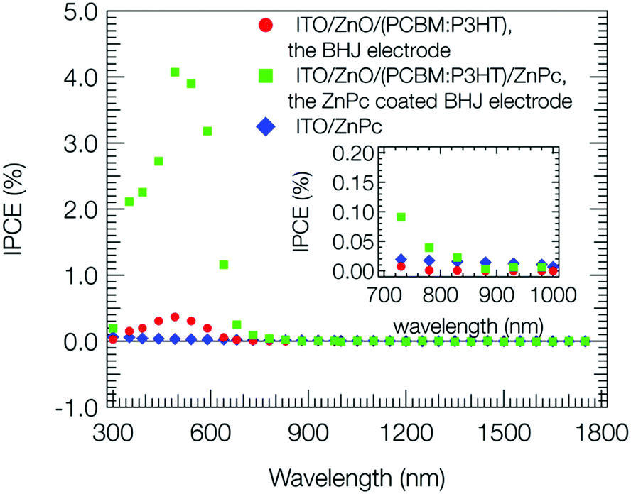 | ||
| Fig. 2 Action spectra of IPCE for the ZnPc (blue), BHJ (red), and ZnPc coated BHJ (green) electrodes. Concentration of thiol, 10 mM (pH = 11); photon flux, 1 × 1016 cm−2 s−1; irradiation side, ITO side; bias, +0.2 V vs. Ag/AgCl. The inset is enlarged view for the near infrared region. | ||
The polarity of these electrodes is discussed for the rest potential change under light illumination as shown in Fig. S8 (ESI†). At the time of light on, both the BHJ electrode and the ZnPc coated BHJ electrode exhibited a shift in the negative potential direction, while ZnPc showed a shift in the positive potential direction, which is a typical p-type semiconductor characteristic.
As shown in Fig. S7 (ESI†), the electrode consisting of ZnPc alone requires the electrode potential of more than +0.1 V vs. Ag/AgCl to exhibit anodic current whether the light illuminates it or not. This means that the Fermi level changes by outer bias to the level of the ZnPc valence band top. Because sufficient amount of holes was produced for the ZnPc coated BHJ electrode under illumination, the anodic polarization of the thin ZnPc layer can be deeper than the ZnPc alone electrode, inducing the oxidation of the thiol via ZnPc. Here we adopted the scanning Kelvin probe microscope (SKPM) technique in order to verify such an anodic polarization on the BHJ and ZnPc coated BHJ electrodes in order to measure the surface potential.44
Fig. 3a and d show topography images for the BHJ and the ZnPc coated BHJ electrodes, respectively. These topographies were consistent with SEM images (Fig. S2b, ESI†) in which sub 100 nm structure was observed. For the same areas of the topography, contact potential difference (VCPD) was observed by the SKPM measurement as shown in Fig. 3b, c, e, and f. For comparison of these samples and conditions, the line profile values are summarized in Fig. 3g and h. The VCPD value is the bias potential between the probe (φprobe) and the sample (φsample) when the Coulomb interaction is nullified between them.44
| VCPD = (φprobe − φsample)/e | (1) |
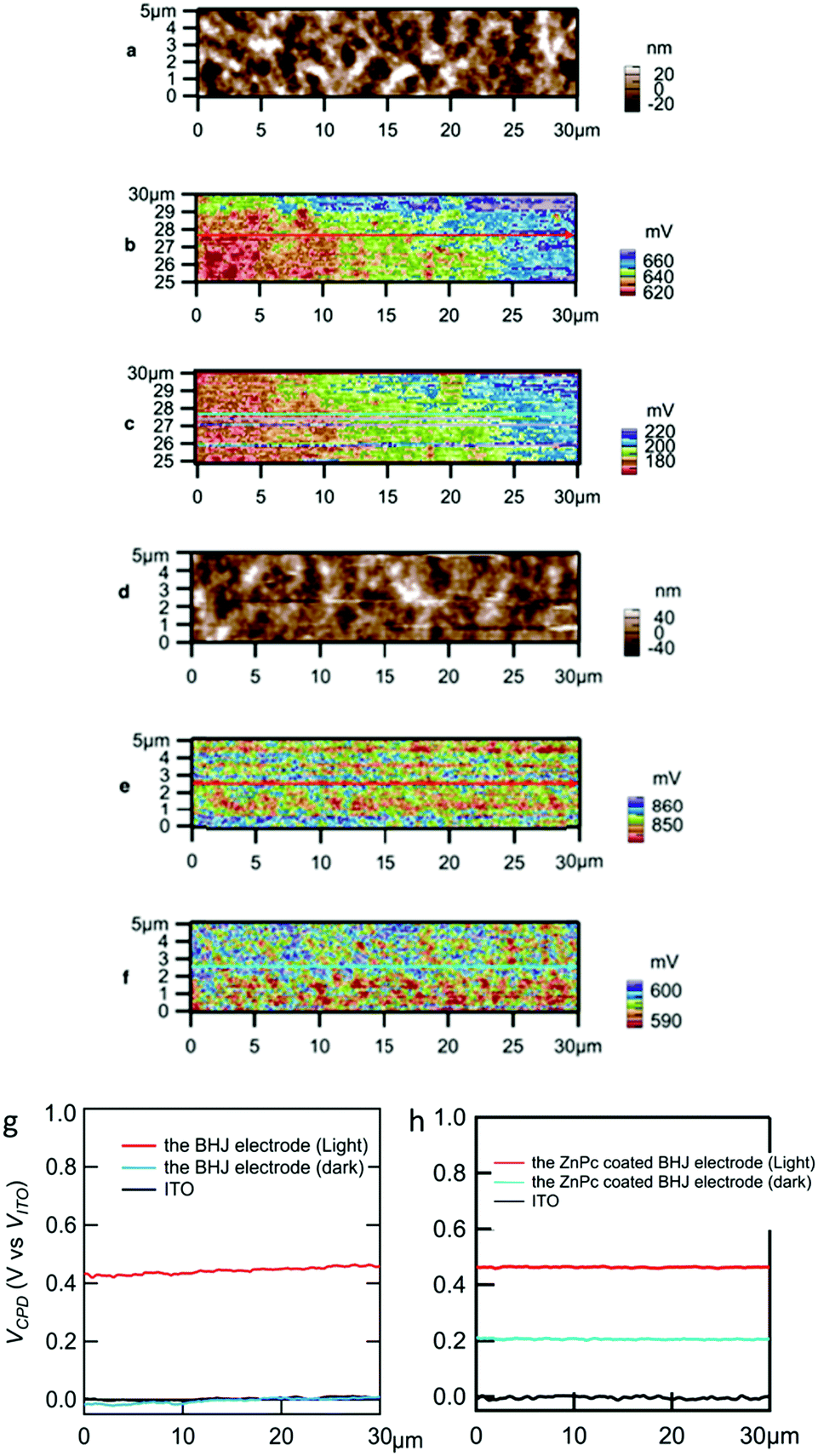 | ||
| Fig. 3 (a) Topography of 30 μm × 5 μm area for the BHJ electrode without ZnPc. SKPM image for the BHJ electrode without ZnPc (b) in the dark and (c) under illumination. (d) Topography for the ZnPc coated BHJ electrode. SKPM image for the ZnPc coated BHJ electrode (e) in the dark and (f) under illumination. Line profile of SKPM versus the potential of ITO, (g) for the BHJ electrode without ZnPc and (h) for the ZnPc coated BHJ electrode. VCPD (vs. VITO) was calculated as the difference between VCPD and VCPD of ITO. | ||
For the conductive sample, the φsample value (in eV) should be equal to the work function (EF, in eV). According to previous studies, φprobe was estimated to be in the range of 4.92–5.6 eV for Pt-coated Ir.45,46 Here, we adopt φprobe = 5.0 eV. The SKPM measurement for ITO/ZnO acting as an electron collection electrode was done by the use of a part surface of the same BHJ electrode or the same ZnPc coated electrode.
The VCPD values of the ITO/ZnO substrates for the BHJ electrode and the ZnPc coated BHJ electrode in the dark were 0.2 V and 0.4 V vs. Pt tip, respectively. Based on eqn (1), φsample for the ITO/ZnO is estimated to be 4.8 eV without ZnPc and 4.6 eV with ZnPc, which are just below the conduction band edge of ZnO. Similarly, φsample values for the BHJ and ZnPc coated BHJ electrodes in the dark were estimated to be 4.8 eV and 4.4 eV, respectively. Fig. S6 (ESI†) shows a potential diagram for the ZnPc coated BHJ electrode in the dark. When coating ZnPc, the positive shift from ITO/ZnO was observed (Fig. 3h), while it does not happen without ZnPc coating (Fig. 3g). Here we discuss the VCPD shifts from that of ITO/ZnO. Generally, the VCPD value depends on substrate surface conditions, while the difference of VCPD from the substrate one to the coating layer one was experimentally repeatable in a previous paper.14 A simple interpretation is a vacuum level shift at the BHJ/ZnPc interface due to hole transfer from BHJ to ZnPc.46,47 The φsample in the dark (φdark) should be constant as shown in Fig. S6 (ESI†) (blue line). This means that an interfacial dipole layer48 consisting of negatively charged BHJ and positively charged ZnPc, which are shown by symbols − and + in Fig. S6 (ESI†), was formed at the BHJ/ZnPc interface.
The actual electrochemical response was enhanced under light illumination especially with ZnPc coating (Fig. 2). Under illumination, the VCPD values were more positive than those in the dark for both ZnPc coating and without coating. From eqn (1), the φsample values were estimated to be 4.3 eV and 4.1 eV for the BHJ and ZnPc coated BHJ electrodes, respectively. Both of the φsample values were shallower than the conduction band edge of ZnO, which was consistent with the photoanodic current generation under illumination. The positive shift of VCPD from the dark condition means hole accumulation at the surface which encountered the (negatively charged) tip without bias. During SKPM measurement, in order to compensate the charge, the bias was applied between sample and tip as VCPD.
As for the ZnPc coated BHJ electrode, the φsample values in the dark were in the middle between those of the ITO/ZnO substrate and under illumination. The reason of the shift in the dark was described above as a vacuum level shift. Furthermore, here a possible factor of charge accumulation at the interface between BHJ and ZnPc would be very long relaxation time after the charge separation process. In various OPV devices, a long relaxation time was reported after light illumination; for example, according to an ESR observation, amorphous TiOx can trap electrons and counter P3HT cation radicals have such a long lifetime.32 The reason is not inconsistent with the above discussion for the vacuum level shift.
To summarize, BHJ films with ZnO as a hole blocking layer were utilized for OPECs after removing the PEDOT:PSS/Au electrode of OPV devices with inverted structures. The ZnO layer was effective in comparison with its absent system for the electron injection from the active BHJ layer to the ITO substrate electrode, resulting in a threshold potential shift to −0.35 V vs. Ag/AgCl for the ZnPc coated BHJ electrode. The effect of ZnPc was clearly observed in the SKPM measurement as an accumulation of the photogenerated holes to ZnPc. Remarkable enhancement of the photoanodic current was observed only by coating of ZnPc, although the potential gain by the BHJ active layer was the same as that without ZnPc as seen in the rest potential change. Since an anodic current by the ZnPc electrode in the dark condition means it functions as a catalyst for thiol oxidation, the remarkable enhancement means that the ZnPc coated on BHJ also effectively functioned as a co-photocatalyst.
We thank the Dynamic Alliance for Open Innovation Bridging Human, Environmental and Materials from MEXT. We also thank the Suzukakedai Materials Analysis Division, Technical Department, Tokyo Institute of Technology, for assistance with SEM analysis and SKPM measurements.
Conflicts of interest
There are no conflicts to declare.References
- O. Inganäs, Adv. Mater., 2018, 30, 1800388 CrossRef PubMed.
- J. T. Kirner and R. G. Finke, J. Mater. Chem. A, 2017, 5, 19560 RSC.
- F. Fumagalli, S. Bellani, M. Schreier, S. Leonardi, H. C. Rojas, A. Ghadirzadeh, G. Tullii, A. Savoini, G. Marra, L. Meda, M. Grätzel, G. Lanzani, M. T. Mayer, M. R. Antognazza and F. Di Fonzo, J. Mater. Chem. A, 2016, 4, 2178 RSC.
- L. Yao, A. Rahmanudin, N. Guijarro and K. Sivula, Adv. Energy Mater., 2018, 8, 1802585 CrossRef.
- L. Steier and S. Holliday, J. Mater. Chem. A, 2018, 6, 21809 RSC.
- C. D. Windle, S. Chandrasekaran, H. Kumagai, G. Sahara, K. Nagai, T. Abe, M. Chavarot-Kerlidou, O. Ishitani and V. Artero, Molecular Design of Photocathode Materials for Hydrogen Evolution and Carbon Dioxide Reduction, in Molecular Technology: Energy Innovation, ed. H. Yamamoto and T. Kato, Wiley, 2018, ch. 10, pp. 251–286 Search PubMed.
- T. Abe, Y. Tanno, N. Taira and K. Nagai, RSC Adv., 2015, 5, 46325 RSC.
- T. Abe, K. Nagai, M. Kaneko, T. Okubo, K. Sekimoto, A. Tajiri and T. Norimatsu, ChemPhysChem, 2004, 5, 716 CrossRef CAS PubMed.
- T. Abe, K. Nagai, M. Kaneko, S. Kabutomori, A. Tajiri and T. Norimatsu, Angew. Chem., Int. Ed., 2006, 45, 2778 CrossRef CAS PubMed.
- L. Wang, D. Yan, D. W. Shaffer, X. Ye, B. H. Layne, J. J. Concepcion, M. Liu and C.-Y. Nam, Chem. Mater., 2018, 30, 324 CrossRef CAS.
- F. C. A. Guerrero, M. Haro, S. Bellani, M. R. Antognazza, L. Meda, S. Gimenez and J. Bisquert, Energy Environ. Sci., 2014, 7, 3666 RSC.
- M. F. Ahmad, T. Abe, C. S. A. Musgrave and K. Nagai, Electrochemistry, 2018, 86, 235 CrossRef CAS.
- T. Abe, S. Miyakushi, K. Nagai and T. Norimatsu, Phys. Chem. Chem. Phys., 2008, 10, 1562 RSC.
- M. F. Ahmad, M. Suzuki, T. Abe and K. Nagai, NPG Asia Mater., 2018, 10, 630 CrossRef CAS.
- T. Abe, M. Ichikawa, T. Hikage, S. Kakuta and K. Nagai, Chem. Phys. Lett., 2012, 549, 77 CrossRef CAS.
- K. Nagai, Y. Yasuda, T. Iyoda and T. Abe, ACS Sustainable Chem. Eng., 2013, 1, 1033 CrossRef CAS.
- K. Nagai, T. Abe, Y. Kaneyasu, Y. Yasuda, I. Kimishima, T. Iyoda and H. Imaya, ChemSusChem, 2011, 4, 727 CrossRef CAS PubMed.
- R. S. Sprick, B. Bonillo, M. Sachs, R. Clowes, J. R. Durrant, D. J. Adamsa and A. I. Cooper, Chem. Commun., 2016, 52, 10008 RSC.
- M. Sachs, R. S. Sprick, D. Pearce, S. A. J. Hillman, A. Monti, A. A. Y. Guilbert, N. J. Brownbill, S. Dimitrov, X. Shi, F. Blanc, M. A. Zwijnenburg, J. Nelson, J. R. Durrant and A. I. Cooper, Nat. Commun., 2018, 9, 4968 CrossRef PubMed.
- S. Yanagida, A. Kabumoto, K. Mizumoto, C.j. Pac and K. Yoshino, J. Chem. Soc., Chem. Commun., 1985, 475 Search PubMed.
- D. Schlettwein, M. Kaneko, A. Yamada, D. Wöhrle and N. I. Jaeger, J. Phys. Chem., 1991, 95, 1748 CrossRef CAS.
- Y. Sahin, S. Alem, R. de Bettignies and J.-M. Nunzi, Thin Solid Films, 2005, 476, 340 CrossRef CAS.
- T. Kuwabara, T. Minami, T. Kusumi, T. Yamaguchi, T. Taima and K. Takahashi, Electrochemistry, 2017, 85, 262 CrossRef CAS.
- R. Steim, S. A. Choulis, P. Schilinsky and C. J. Brabec, Appl. Phys. Lett., 2008, 92, 093303 CrossRef.
- H. Schmidt, H. Flugge, T. Winkler, T. Bulow, T. Riedl and W. Kowalsky, Appl. Phys. Lett., 2009, 94, 243302 CrossRef.
- S. K. Hau, H.-L. Yip, H. Ma and A. K.-Y. Jen, Appl. Phys. Lett., 2008, 93, 233304 CrossRef.
- A. Hayakawa, O. Yoshikawa, T. Fujieda, K. Uehara and S. Yoshikawa, Appl. Phys. Lett., 2007, 90, 163517 CrossRef.
- J. Y. Kim, K. Lee, N. E. Coates, D. Moses, T.-Q. Nguyen, M. Dante and A. J. Heeger, Science, 2007, 317, 222 CrossRef CAS PubMed.
- G. K. Mor, K. Shankar, M. Paulose, O. K. Varghese and C. A. Grimes, Appl. Phys. Lett., 2007, 91, 152111 CrossRef.
- T. Kuwabara, T. Nakayama, K. Uozumi, T. Yamaguchi and K. Takahashi, Sol. Energy Mater. Sol. Cells, 2008, 92, 1476 CrossRef CAS.
- T. Kuwabara, H. Sugiyama, M. Kuzuba, T. Yamaguchi and K. Takahashi, Org. Electron., 2010, 11, 1136 CrossRef CAS.
- T. Kuwabara, K. Yano, K. Takahashi, D. Son and K. Marumoto, J. Phys. Chem. C, 2015, 119, 5274 CrossRef CAS.
- E. Itoh, S. Sakai and K. Fukuda, Jpn. J. Appl. Phys., 2018, 57, 03EJ07 CrossRef.
- K. Takanezawa, K. Tajima and K. Hashimoto, Appl. Phys. Lett., 2008, 93, 063308 CrossRef.
- T. Fukuda and Y. Uratani, Electrochemistry, 2017, 85, 249 CrossRef CAS.
- D. Li, W.-j. Qin, S.-c. Zhang, D.-y. Liu, Z.-y. Yu, J. Mao, L.-f. Wu, L.-y. Yang and S.-g. Yin, RSC Adv., 2017, 7, 6040 RSC.
- B. Wu, Z.-h. Wu, Q.-y. Yang, F.-r. Zhu, T.-W. Ng, C.-S. Lee, S.-H. Cheung and S.-K. So, ACS Appl. Mater. Interfaces, 2016, 8, 14717 CrossRef CAS PubMed.
- T. Kuwabara, Y. Omura, K. Takahashi, V. Vohra and H. Murata, J. Phys. Chem. C, 2014, 118, 4050 CrossRef CAS.
- T. Kuwabara, M. Nakamoto, Y. Kawahara, T. Yamaguchi and K. Takahashi, J. Appl. Phys., 2009, 105, 124513 CrossRef.
- M. Karakawa, N. Ohmae, T. Nagai, T. Kusumi, T. Kuwabara, T. Taima, T. Yamaguchi and K. Takahashi, Org. Electron., 2019, 66, 76 CrossRef CAS.
- J. Bian, J. Feng, Z. Zhang, Z. Li, Y. Zhang, Y. Liu, S. Ali, Y. Qu, L. Bai, J. Xie, D. Tang, X. Li, F. Bai, J. Tang and L. Jing, Angew. Chem., Int. Ed., 2019, 58, 10873 CrossRef CAS PubMed.
- S. Zhang, P. Arunachalam, T. Abe, T. Iyoda and K. Nagai, J. Photochem. Photobiol., A, 2012, 244, 18 CrossRef CAS.
- P. Arunachalam, S. Zhang, T. Abe, M. Komura, T. Iyoda and K. Nagai, Appl. Catal., B, 2016, 193, 240 CrossRef CAS.
- Kelvin Probe Force Microscopy, ed. S. Sadewasser and T. Glatzel, Springer Series in Surface Science, 2011, vol. 48, p. 12 Search PubMed.
- D. Yamashita and A. Ishizaki, Appl. Surf. Sci., 2016, 363, 240 CrossRef CAS.
- F. Yan, G. Chen, L. Lu and J. E. Spanier, ACS Nano, 2012, 6, 2353 CrossRef CAS PubMed.
- D. J. Ellison, J. Y. Kim, D. M. Stevens and C. D. Frisbie, J. Am. Chem. Soc., 2011, 133, 13802 CrossRef CAS PubMed.
- H. Ishii, K. Sugiyama, E. Ito and K. Seki, Adv. Mater., 1999, 11, 605 CrossRef CAS.
Footnotes |
| † Electronic supplementary information (ESI) available. See DOI: 10.1039/c9cc04759j |
| ‡ Passed away on Dec. 5, 2017. |
| This journal is © The Royal Society of Chemistry 2019 |