
 Open Access Article
 This Open Access Article is licensed under a
 Creative Commons Attribution 3.0 Unported Licence
Key factors affecting photoelectrochemical performance of g-C3N4 polymer films†
Qiushi
Ruan
 a,
Mustafa K.
Bayazit
ab,
Vankayala
Kiran
ac,
Jijia
Xie
a,
Yiou
Wang
ad and
Junwang
Tang
*a
a,
Mustafa K.
Bayazit
ab,
Vankayala
Kiran
ac,
Jijia
Xie
a,
Yiou
Wang
ad and
Junwang
Tang
*a
aSolar Energy & Advanced Materials Research Group, Department of Chemical Engineering, UCL Torrington Place, London, WC1E 7JE, UK. E-mail: junwang.tang@ucl.ac.uk
bSabanci University Nanotechnology Research and Application Center, 34956, Tuzla, Istanbul, Turkey
cDepartment of Chemistry, BITS Pilani, K. K. Birla Goa Campus, Goa 403 726, India
dChair for Photonics and Optoelectronics, Nano-Institute Munich, Ludwig-Maximilians-Universität München, Königinstr. 10, 80539 Munich, Germany
First published on 28th May 2019
Abstract
We investigated the relationship between crystallinity, deep trap states and PEC performance of g-C3N4 photoelectrodes. Long-lived charge carriers were present in the more poorly crystalline samples, due to deeper trap states, which inversely correlated with photoelectrochemical performance. The charge diffusion length in a compact g-C3N4 film was determined to be ca. 1000 nm.
The benchmark polymer photocatalyst g-C3N4 has attracted great attention due to its ease of processing, readily tunable band structure, very promising activity in suspension systems and being composed of abundant elements.1 The fabrication of active g-C3N4 films has, as a result of these properties and the large-scale industrial use of such films, become a preferred area of research. The g-C3N4 films prepared so far, however, show only moderate photoelectrochemical performances, despite attempts to improve their performances.2–4 In contrast, the powder form has shown success in suspension systems as reported earlier.5 This moderate photoelectrochemical performance of g-C3N4 films has been speculated to be due to factors such as its poor charge separation, low electronic conductivity and small charge diffusion length.3 Obviously, clear and comprehensive insight into this issue is highly sought after.
Charge diffusion length has been observed to play a pivotal role in determining the quality of photocurrents and photoelectrochemical performance. For instance, the well-studied oxide film α-Fe2O3 was shown to suffer from unsatisfactory photocurrents despite its very good light absorption.6 A comprehensive investigation by Grätzel et al. revealed the key issue here to be the short charge diffusion length (∼2–4 nm); such a feature explained the very good performance of nanostructured, dendrite α-Fe2O3 films composed of rods with lengths of just a few nanometers, with this good performance specifically due to their shorter distances for electrons to migrate than found for bulk α-Fe2O3 films.7,8 Charge diffusion length is also believed to be an important factor in g-C3N4 in terms of charge separation, migration and surface reactions; the other factor heavily influencing photoelectrode performance is charge separation and recombination influenced predominantly by trap states in the bulk or on the surface of a semiconductor.9,10
Our previous study related to charge trapping in g-C3N4 powders in a suspension system showed that a high concentration of electrons were deeply trapped by electron acceptors in g-C3N4 and remained unreactive.11 These photogenerated electrons with long lifetimes can participate neither in photocatalytic reactions nor photoluminescence. It was also reported that the structural disorder in g-C3N4 could introduce both shallow and deep trap states, with the shallow ones positively contributing to its photocatalytic performance.10 The understanding of the impact of trap states on the activity of g-C3N4, while informative, was achieved in a powder-suspension system. In a PEC system where the directional charge migration is vital, the presence of many deep trap states would prohibit the directional charge transport and affect the charge diffusion length. The influences of both charge diffusion length and trap states on the performance of g-C3N4 photoelectrodes are very important but not yet well understood. Peng et al. has reported a remarkable charge diffusion length of up to 36 μm in g-C3N4/rGO films; but without rGO, diffusion length would be a factor limiting the PEC performance of g-C3N4.12 It is thus necessary to investigate the trap state conditions in g-C3N4 and their influence on charge diffusion length.
It is speculated that deep trap states in g-C3N4 may be caused by terminal groups or defects.11 A desired closely packed and well-crystallized g-C3N4 thin film in principle is expected to reduce the quantity of deep trap states and hence facilitate the charge transfer with a suitable charge diffusion length.13,14 To explore the influence of trap states on the PEC performance of g-C3N4 films, here we fabricated three kinds of g-C3N4 films with different trap state conditions, including bulk-g-C3N4 film, porous-g-C3N4 film and the compact-g-C3N4 film previously reported by our group.3 The trap state conditions were determined using the open circuit photovoltage decay (OCVD) technique, and charge diffusion length was measured by taking a small perturbation photovoltage transient (TPV) measurement.
The acquired XRD patterns are shown in Fig. 1a. All samples yielded a main peak located at about 27.5°, attributed to the interlayer arrangement of the graphite-like structure. A weaker peak was observed at 13.0° and was attributed to the heptazine units in the g-C3N4 structure.15 The FWHM values of the peak at 27.5° for the bulk, porous, and compact g-C3N4 films were measured to be 1.0°, 1.1° and 0.7°, respectively. Since a small FWHM indicates high crystallinity, these results indicated a more ordered layer structure for the compact g-C3N4 film than for the bulk and porous g-C3N4 films. Raman spectra of all three samples, shown in Fig. 1b, were also acquired to confirm the level of order in each structure. For g-C3N4, the ratio of the intensity of the D band (located at 1405 cm−1) to that of the G band (at 1570 cm−1), abbreviated as ID/IG, could illustrate the distortion of the crystal structure and the defect conditions.16 Analysis of the Raman spectra displayed in Fig. S2 (ESI†) and summarized in Table 1 showed ID/IG increasing from 0.13 for the compact-g-C3N4 sample to 0.41 for bulk-g-C3N4 and to 0.55 for porous-g-C3N4. These results suggested the least structural distortion for compact-g-C3N4 and the most defect densities for the bulk and especially porous g-C3N4 samples, consistent with the XRD analysis.
 | ||
| Fig. 1 (a) XRD patterns and (b) Raman spectra of the bulk, compact, and porous g-C3N4 films. | ||
| Porous-g-C3N4 | Bulk-g-C3N4 | Compact-g-C3N4 | |
|---|---|---|---|
| XRD(FWHM) | 1.1° | 1.0° | 0.7° |
| I D/IG | 0.55 | 0.41 | 0.13 |
SEM, UV-Vis and FT-IR spectra of all three samples, displayed in Fig. S3–S5 (ESI†), were acquired in order to characterize their morphologies, light absorption properties and structures. XPS spectra were also analyzed, and are displayed in Fig. S6 (ESI†). The N1s region of the XPS spectrum can be fitted by three components. The main peak located at 398.7 eV was attributed to C–N–C bonds. The other two peaks at higher energy accounted for C–[N]3 (399.9 eV) and C–NHx bonds (401.1 eV) respectively.17 The percentage breakdown of different bonds is listed in Table S1 (ESI†). The percentages of the compact, bulk, and porous g-C3N4 films consisting of C–NHx, recognized as forming the terminal groups of the g-C3N4 structure, were determined to be 8%, 13.6% and 18.8%, respectively. That is, the more ordered g-C3N4 structure showed a lower percentage of terminal groups (C–NHx), and hence the structure of compact-g-C3N4 was most complete and that of porous-g-C3N4 least complete, in agreement with the XRD and Raman analyses.
To understand the fate of the trap states in the three samples, charge dynamics were investigated by taking OCVD measurements, which has proven to be a useful way to characterize the trap state conditions in photoelectrodes regardless of surface area.18,19 The average time elapsed between the generation and recombination of the electrons (average charge lifetime) was determined by fitting a biexponential function to the decay curve (Fig. 2 and Fig. S7, ESI†).18
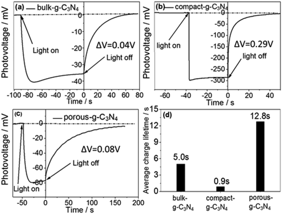 | ||
| Fig. 2 Open circuit voltage decay (OCVD) plots of (a) bulk g-C3N4, (b) compact g-C3N4, and (c) porous g-C3N4 with 150 W xenon lamp illumination from the electrolyte–electrode (EE) side. (d) Calculated average charge lifetimes in the g-C3N4 films. (Generated photovoltage ΔV is the difference in voltage between dark and illumination conditions.). | ||
Photovoltage decay in the compact-g-C3N4 sample was much faster than in the other two samples. Specifically, the average lifetimes of the electrons were found to be 0.9 s, 5.0 s and 12.8 s for the compact, bulk, and porous g-C3N4 samples, respectively. The rapid photovoltage decay or short average lifetime indicated that electrons rapidly recombined with holes in the absence of an electron donor in the electrolyte, while the long lifetimes of electrons observed in the other samples were mainly due to a severe electron trap effect.18 Most long-lifetime electrons in such samples are trapped at deep levels and located at low energy levels (more positive levels) that are insufficient to participate in redox reactions.11 These deep trap states can also hinder the migration of electrons in a photoelectrode. As photogenerated electrons tend to migrate from the conduction band to the deep trap states after excitation, reducing the deep trap state density can promote the charge transfer efficiency, thereby enhancing the photocurrent density of a photoelectrode. Apparently, the significantly reduced average lifetime in the compact-g-C3N4 film (0.9 s) indicated that the majority of photogenerated electrons were less likely deeply trapped here than in the bulk g-C3N4 sample (5.0 s) and porous g-C3N4 sample (12.8 s). Also, the long average electron lifetime in the porous-g-C3N4 sample (12.8 s) suggested the presence of very deep electron-trapping states. Therefore, for the samples investigated, the degree of the crystallinity showed an inverse relationship with the quantity of trap states.
More information about the trap state conditions was extracted from the photovoltage (ΔV), shown in Fig. 2. The photovoltage generated in the compact-g-C3N4 sample, (ΔV = 0.29 V) was much larger than those in the bulk and porous g-C3N4 films (ΔV < 0.1 V). Since low photovoltage (ΔV) is believed to be related to deep defects,20,21 the higher photovoltage generated in the compact g-C3N4 sample indicated that its density of deep defects was much less than those in the bulk and porous g-C3N4 films.
The results described so far indicated a clear relationship between trap-state conditions and crystallinity of the g-C3N4 films. The compact-g-C3N4 film with the most ordered structure mainly consisted of shallow trap states, resulting in the shortest average electron lifetime (0.9 s) and highest photovoltage (0.29 V) of all three samples. In contrast, both the bulk g-C3N4 film and porous g-C3N4 film included deep trap states due to their low crystallinity levels, leading to long charge lifetimes (5.0 s for the bulk g-C3N4 film and 12.8 s for the porous g-C3N4 film), which limited the charge transfer and resulted in low photovoltages (0.04 V for the bulk g-C3N4 film and 0.08 V for the porous g-C3N4 film).
The PEC performances of the three samples were examined in a PEC system and the results are shown in Fig. 3. The compact g-C3N4 film exhibited the highest anodic photocurrent density (e.g., 180 μA cm−2 at 0.6 V vs. Ag/AgCl) of the three photoelectrodes, apparently due to its significantly reduced deep trap-state density caused by high crystallinity and uniform morphology. In contrast, the bulk and porous g-C3N4 films, each with a low crystallinity and rough morphology resulting in deeper trap states, exhibited less than a 30 times lower photocurrent density (5 μA cm−2 at 0.6 V vs. Ag/AgCl). This result revealed that significantly reducing the density of deep trap states in g-C3N4 films could help improve charge transfer across the film and facilitate charge collection on the electrode and electrolyte interface, resulting in a significantly enhanced photoelectrochemical performance. The stability of compact g-C3N4 is shown in Fig. S8 (ESI†). At +0.1 V vs. Ag/AgCl, the photocurrent density was roughly stable at 65 μA cm−2.
 | ||
| Fig. 3 Plots of photocurrent density vs. potential for the (a) bulk-g-C3N4 film, (b) compact-g-C3N4 film and (c) porous-g-C3N4 film using a 150 W xenon lamp illuminating the substrate–electrode (SE) side, electrolyte: 0.1 M Na2SO4, pH = 6.5. | ||
Charge diffusion length is a key factor that determines photoelectrode performance. A long charge diffusion path guarantees efficient charge transfer across the electrode. Metal oxide photoelectrodes made of different materials often show different diffusion lengths. For example, TiO2 has an ∼10 micrometer diffusion length,22 while Fe2O3 has a much smaller diffusion length of 2–4 nm.7,8 The charge diffusion lengths of polymer photoelectrodes have been much less extensively investigated. TPV is herein used to determine this important factor for the g-C3N4 film. The photovoltage rise and decay corresponding to pulsed light were recorded and the electron diffusion length was derived as described as follows.
The electron diffusion length for the compact-g-C3N4 film was measured under a range of light intensities modulated by varying the LED light power (25–100 W). We were able to vary the amplitude of the transient photovoltage between 5 mV and 20 mV by tuning the output power of the LED light. Time constants for photovoltage rise (τrise) and decay (τn) were determined by using the initial phase of the photovoltage rise and decay, as shown in Fig. 4a. The duration of the pulse light was 1 ms. As shown in Fig. 4b, the corresponding τrise and τn were calculated using eqn (a) and the resultant electron diffusion length (L) was then determined by using eqn (b) and (c) in ESI.†22,23
 | ||
| Fig. 4 (a) Transient photovoltage vs. time plots at various illumination power values, and (b) dependence of photovoltage rise time (τrise), effective electron lifetime (τn) and charge diffusion length on illumination power for the compact-g-C3N4 sample. | ||
The effective electron lifetime (τn) was observed to decrease with increasing illumination power, specifically from 950 ms at 25 W to 350 ms at 100 W. With high light intensity, the reduced electron lifetime was due to an increased rate of recombination of electron–hole pairs.24 As expected, though a series of pulse light intensities resulted in different values of τrise and τn, the electron diffusion length was determined to be ca. 1000 nm. A TPV measurement was performed on another sample, S1, to check the reproducibility of the diffusion length. The thickness of sample S1 was ca. 800 nm (Fig. S10, ESI†) and the charge diffusion length was derived again to be close to 1000 nm (Fig. S11, ESI†), very close to that of the compact g-C3N4 sample. Taking into account the thickness of the compact g-C3N4 film (600 nm), such a considerable electron diffusion length could guarantee efficient charge transfer and collection across the photoelectrode, which significantly contributed to its excellent PEC performance. To further confirm our measurement of the electron diffusion length in compact g-C3N4, the photocurrent densities of films with different thicknesses were compared by illuminating them on their front and back sides (Fig. S12, ESI†). For a thin film (ca. 500 nm) with a thickness much less than the calculated electron diffusion length (1000 nm), the illumination of the front side gave a photocurrent density a little bit higher than that achieved by illuminating the back side, demonstrating the ability of all photoelectrons to traverse the film. However, when the film thickness was close to the electron diffusion length (such as ca. 900 nm), the illumination of the front side yielded a 40% lower photocurrent density at 1.0 V vs. Ag/AgCl than did the illumination of the back side, attributed to an inability of some of the electrons to move across the film. In addition, TPV measurements on the bulk and porous g-C3N4 samples showed neither a reliable nor reproducible response. A presence of many deep trap states is believed to result in a severe decrease in the charge diffusion length, causing difficulties in taking such measurements using this technology. It is worth noticing that g-C3N4 has a 2D structure, whose charge diffusion length may be highly directional (diffusion length may be different in the plane or across stacks of structures). And the XRD pattern of the compact g-C3N4 sample did not indicate a highly orientated crystal lattice (Fig. 1a). We believe that the g-C3N4 polycrystalline sample was randomly orientated and the electron diffusion length obtained was on average isotropic.
In summary, we have demonstrated a good relationship between crystallinity and the trap states in g-C3N4. Worse crystallinity was concluded to result in deeper trap states, which would lead to unusually long-lived charge carriers that do not guarantee good photoelectrochemical performance. Low trap-state density and long electron diffusion paths could be achieved in g-C3N4 photoelectrodes by manipulating its crystallinity. The significantly shortened charge lifetime and large transient photovoltage illustrated the low trap state density in a well-crystallized, closely packed, high-quality g-C3N4 electrode. The charge diffusion length in this g-C3N4 photoelectrode was determined to be ca. 1000 nm. The reduced deep trap state density and the long electron diffusion path finally contributed to a facilitated charge transfer, efficient charge collection across the electrode, and photocurrent density of 180 μA cm−2, 30 times greater than that of the bulk g-C3N4 photoelectrode prepared using g-C3N4 powders. This study underscored the effect of trap states on the PEC performance of our g-C3N4 benchmark polymer photocatalyst and determined its electron diffusion length. We expect the results of this study to further encourage future mechanistic studies of highly efficient polymer photoelectrodes for photosynthesis.
Conflicts of interest
There are no conflicts to declare.References
- X. Wang, K. Maeda, A. Thomas, K. Takanabe, G. Xin, J. M. Carlsson, K. Domen and M. Antonietti, Nat. Mater., 2009, 8, 76 CrossRef CAS PubMed
.
- Q. Ruan, W. Luo, J. Xie, Y. Wang, X. Liu, Z. Bai, C. J. Carmalt and J. Tang, Angew. Chem., Int. Ed., 2017, 56, 8221–8225 CrossRef CAS PubMed
- Y. Fang, Y. Xu, X. Li, Y. Ma and X. Wang, Angew. Chem., 2018, 57, 9749–9753 CrossRef CAS PubMed
- M. Volokh, G. Peng, J. Barrio and M. Shalom, Angew. Chem., Int. Ed., 2018, 57, 1186–1192 CrossRef PubMed
- L. Lin, Z. Yu and X. Wang, Angew. Chem., Int. Ed., 2018, 58, 6164–6175 CrossRef PubMed
- C. Jorand Sartoretti, B. D. Alexander, R. Solarska, I. A. Rutkowska, J. Augustynski and R. Cerny, J. Phys. Chem. B, 2005, 109, 13685–13692 CrossRef PubMed
- I. Cesar, A. Kay, J. A. Gonzalez Martinez and M. Grätzel, J. Am. Chem. Soc., 2006, 128, 4582–4583 CrossRef CAS PubMed
- A. Kay, I. Cesar and M. Grätzel, J. Am. Chem. Soc., 2006, 128, 15714–15721 CrossRef CAS PubMed
- J. Ran, T. Y. Ma, G. Gao, X.-W. Du and S. Z. Qiao, Energy Environ. Sci., 2015, 8, 3708–3717 RSC
- T. Maschmeyer, X. Li, I. Sergeyev, F. Aussenac, A. Masters and J. Hook, Angew. Chem., 2018, 130, 6964–6968 CrossRef
- R. Godin, Y. Wang, M. A. Zwijnenburg, J. Tang and J. R. Durrant, J. Am. Chem. Soc., 2017, 139, 5216–5224 CrossRef CAS PubMed
- G. Peng, M. Volokh, J. Tzadikov, J. Sun and M. Shalom, Adv. Energy Mater., 2018, 8, 1800566 CrossRef
- G. Peng, J. Albero, H. Garcia and M. Shalom, Angew. Chem., 2018, 130, 16033–16037 CrossRef
- G. Peng, J. Qin, M. Volokh, C. Liu and M. Shalom, J. Mater. Chem. A, 2019, 7, 11718–11723 RSC
- R. Wang, H. Liu, Z. Fan, L. Li, Y. Cai, G. Xu, W. Luo, B. Yang, Y. Zhou and Z. Zou, Nanoscale, 2018, 10, 3342–3349 RSC
- H. Wang, X. Zhang, J. Xie, J. Zhang, P. Ma, B. Pan and Y. Xie, Nanoscale, 2015, 7, 5152–5156 RSC
- Y. Wang, M. K. Bayazit, S. J. Moniz, Q. Ruan, C. C. Lau, N. Martsinovich and J. Tang, Energy Environ. Sci., 2017, 10, 1643–1651 RSC
- Y.-C. Pu, G. Wang, K.-D. Chang, Y. Ling, Y.-K. Lin, B. C. Fitzmorris, C.-M. Liu, X. Lu, Y. Tong and J. Z. Zhang, Nano Lett., 2013, 13, 3817–3823 CrossRef CAS PubMed
- W. Liu, L. Cao, W. Cheng, Y. Cao, X. Liu, W. Zhang, X. Mou, L. Jin, X. Zheng and W. Che, Angew. Chem., Int. Ed., 2017, 56, 9312–9317 CrossRef CAS PubMed
- W. Tress, M. Yavari, K. Domanski, P. Yadav, B. Niesen, J. P. C. Baena, A. Hagfeldt and M. Graetzel, Science, 2018, 11, 151–165 CAS
- W. Tress, M. Yavari, K. Domanski, P. Yadav, B. Niesen, J. P. C. Baena, A. Hagfeldt and M. Graetze, Energy Environ. Sci, 2018, 11, 151–165 RSC
- W. Leng, P. R. Barnes, M. Juozapavicius, B. C. O’Regan and J. R. Durrant, J. Phys. Chem. Lett., 2010, 1, 967–972 CrossRef CAS
- B. C. O'Regan, K. Bakker, J. Kroeze, H. Smit, P. Sommeling and J. R. Durrant, J. Phys. Chem. B, 2006, 110, 17155–17160 CrossRef PubMed
- J. Tang, J. R. Durrant and D. R. Klug, J. Am. Chem. Soc., 2008, 130, 13885–13891 CrossRef CAS PubMed
Footnote |
| † Electronic supplementary information (ESI) available. See DOI: 10.1039/c9cc03084k |
| This journal is © The Royal Society of Chemistry 2019 |