
Atomic layer deposition for efficient and stable perovskite solar cells
Seongrok
Seo
a,
Seonghwa
Jeong
a,
Hyoungmin
Park
a,
Hyunjung
Shin
 *a and
Nam-Gyu
Park
*b
*a and
Nam-Gyu
Park
*b
aDepartment of Energy Science, Sungkyunkwan University, Suwon 440-746, Republic of Korea. E-mail: hshin@skku.edu
bSchool of Chemical Engineering, Sungkyunkwan University, Suwon 440-746, Republic of Korea. E-mail: npark@skku.edu
First published on 21st January 2019
Abstract
Organic–inorganic hybrid metal halides are now the most attractive photovoltaic absorber materials, typically, methylammonium lead triiodides (MAPbI3). These unique semiconducting materials as absorbers demonstrate a remarkably improved power conversion efficiency of over 20% and now with a certified efficiency of 23.3%. Considering the Shockley–Queisser limit and their bandgaps, there is still much room to increase the efficiency. Stable devices with reproducibility and long-term use are essential for their commercialization. Atomic layer deposition (ALD) is a powerful technique to deposit high-quality thin films with excellent thickness accuracy and conformality, as well as with no pin-holes in a large area at low temperatures. ALD could be an ideal tool for efficient and stable perovskite solar cells. In particular, ALD will emerge for the production of tandem as well as flexible solar cells. This review contains the following recent research topics; underlying charge transport layers onto transparent conducting oxides (TCO), interfacial layers, overlying electron transport layers (ETLs), and encapsulation techniques utilized by ALD. Several extended understandings by recent studies and challenges toward further enhancing the efficiency and stability will be addressed.
1. Introduction
Organic–inorganic hybrid metal halides are now emerging as a new class of semiconductors. Known as the ‘perovskite solar cell (PSC)’, photovoltaic (PV) cells with MAPbI3 (methyl ammonium lead triiodides), a notable example of a hybrid metal halide, as light-absorbing materials showed a remarkable power conversion efficiency (PCE) of over 20%.1–11 The certified PCE is currently 23.3%.12 PSCs have attracted considerable attention due to their rapid increase in absolute efficiency per year (%) of 2.27 from that of the first solid-state PSCs of 9.7%3 up to the currently highest certified PSC within recent six years, which has largely surpassed other types of solar cells, increasing by under 1.0% per year.12 The PCE enhancements were achieved through scientific understanding as well as by engineering advancement. The former includes crystal growth, compositional modification and optoelectronic properties of the perovskite film, and the latter signifies interfacial modification and the development of highly efficient charge transport layers (CTLs) in the cells.13–16PSCs have a sandwich structure of the perovskite layer, which absorbs sunlight and generates photo-excited carriers, and CTLs, which transport the photo-excited carriers to the electrodes. In addition, CTLs are divided into electron transport layers (ETLs), which transport photo-excited electrons, and hole transport layers (HTLs), which transport holes. The typical structures of PSCs can be represented by three different types as shown in Fig. 1, which are mesoscopic n–i–p, planar n–i–p and p–i–n structures, respectively, and the types of PSCs are named according to the CTLs in which the sunlight passes through first. In the mesoscopic structure, a bilayer using a compact layer and a nanostructured/mesoporous material is used as an ETL, whereas in a planar structure, only a compact layer is used as CTLs. Since the ETL extracts and transport electrons, n-type materials were used, and the conduction band (CB) minimum should be positioned lower than that of the perovskite. On the other hand, the HTL requires p-type materials, and the valence band (VB) maximum must be shallower than that of the perovskite. Most typical n–i–p PSCs include TiO2 as ETL and 2,2′,7,7′-tetrakis(N,N-bis(p-methoxyphenyl)amino)-9,9′-spirobifluorene (Spiro-OMeTAD) as the HTL, and the p–i–n includes poly(3,4-ethylenedioxythiophene):poly(styrene-sulfonate) (PEDOT:PSS), poly[bis(4-phenyl)(2,4,6-trimethylphenyl)amine] (PTAA) and 1-(3-methoxycarbonyl)propyl-1-phenyl[6,6]C61 (PCBM). Inorganic materials have been intensively studied as CTLs to enhance the stability of PSCs. Representative inorganic materials of ETLs include TiO2,14 SnO2,17 ZnO,18 Zn2SnO419 and BaSnO3,20 and those of HTLs include NiO,21 CuOx,22 CuI,23 CrOx,24 Cu-based delafossite materials25–27 and high-work-function MoO3.28 Among the many candidates, ETLs such as TiO2, SnO2, ZnO and NiO HTL layers can be deposited through atomic layer deposition (ALD) processes; in addition, Al2O3 which does not act as a CTL due to its insulating property but is used as a passivation layer, is also capable of ALD processes.29,30
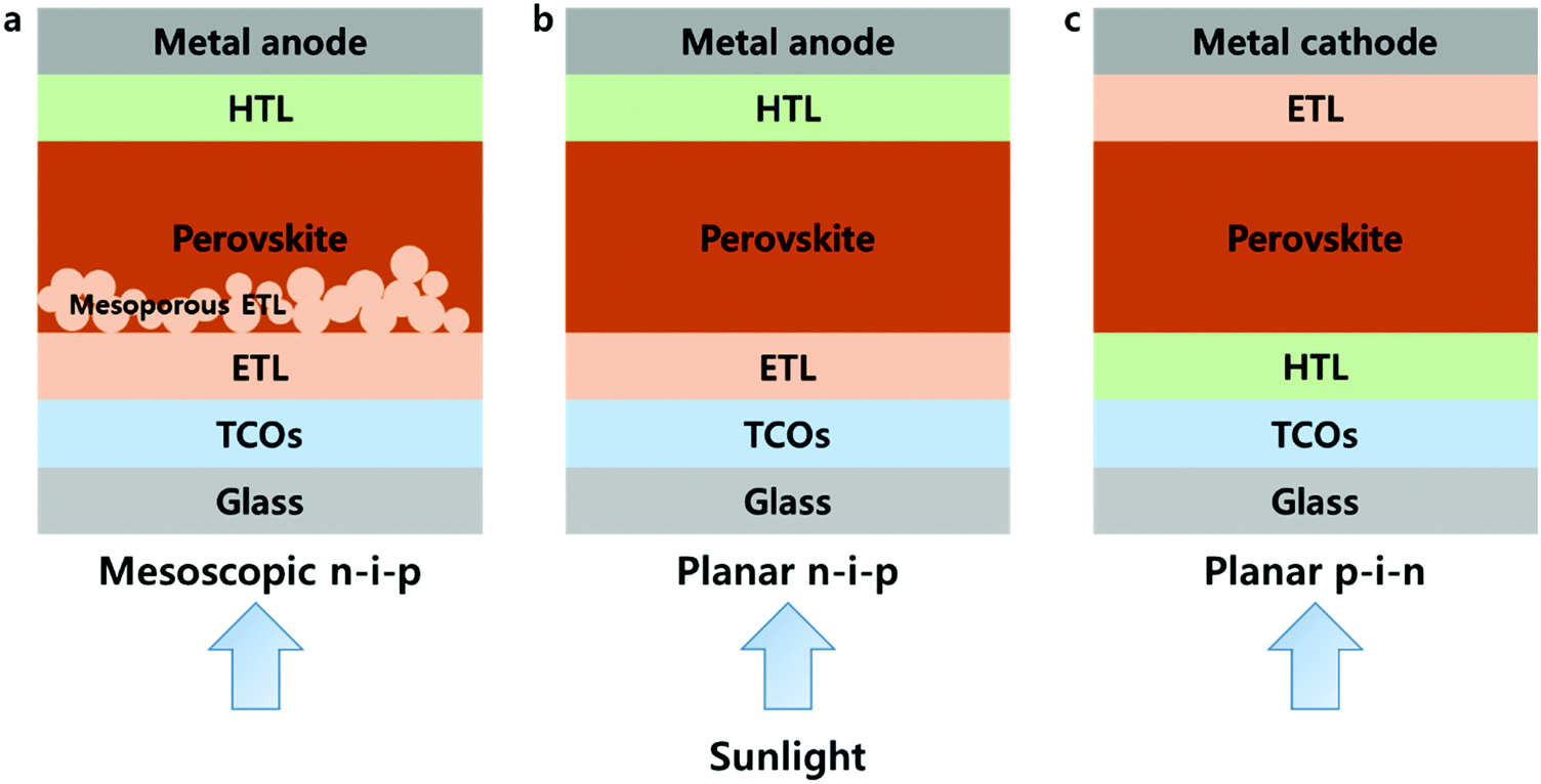 | ||
| Fig. 1 Typical three structures of the PSCs. The bilayer of compact and mesoporous materials consists of the ETL in mesoscopic n–i–p structure (a), and only compact ETL and HTL are used in planar n–i–p structure (b) and p–i–n structure (c). | ||
ALD is a powerful tool to deposit films on the substrates, with a high conformality that can be hardly achieved by any other technique. Dr Tuomo Suntola first invented atomic layer epitaxy (ALE, commonly used term prior to 2000, instead of ALD) in the 1970s.31 In his paper, the development of electroluminescent flat panel displays using ZnS thin films grown via ALE was reported.2 During the past decades after the invention, enormous materials as well as growth methods via ALD have been developed.32 The application of ALD has been largely devoted to the microelectronic industry and nanotechnology.32 In recent, many studies have focused on the application of ALD to renewable energy devices including photovoltaics (PVs).33,34
ALD is comprised of a binary sequence of self-limiting chemical reactions between gas-phase precursor molecules and a solid surface, which is solely dependent on the properties of the surface. This self-limiting nature of the ALD gives rise to conformal growth behavior and additional control over the total thickness of the film. The precise film thickness control can be realized simply by the repeating number of coating cycles. The schematic typical ALD process is described in Fig. 2. A cycle of the ALD process consists of four steps: the A source pulse, purging and the B source pulse, and purging. Injecting the A source into the reaction chamber together with the carrier gas (usu. N2, Ar, etc.) causes the A molecule (Zn(CH2CH2)2 (diethylzinc, DEZ), Al(CH3)3 (trimethylaluminium, TMA), etc.) to be chemisorbed on the substrate, and then injecting the B (H2O, H2O2, H2S, etc.) source into the substrate induces a self-limiting reaction between the chemisorbed A and B sources. The remaining surplus B sources will be removed through purging. The self-limiting reaction refers to the reaction of the reactant sources A and B only on the surfaces, not the reaction between sources off of the surface. We briefly introduce the surface chemistry of Al2O3 using TMA and H2O in ALD, which was well-established as a model system:35
| (A) –AlOH* + Al(CH3)3 → AlOAl(CH3)2* + CH4(g) | (1) |
| (B) –AlCH3* + H2O → AlOH* + CH4(g) | (2) |
| (C) 2Al(CH3)3 + 3H2O → Al2O3 + 3CH4(g) ΔH = −376 kcal | (3) |
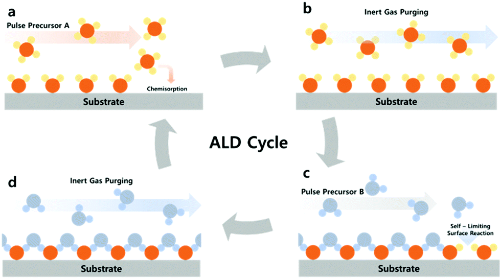 | ||
| Fig. 2 Schematic representation of the typical ALD process; (a and c) A and B source precursor pulse; (b and d) inert gas purging of the remaining (unreacted) precursor source. | ||
Taking advantages of the self-limiting chemical surface reactions, ALD can guarantee high uniformity in a large area, conformality and a nm scale thickness control of films. Furthermore, ultra-high aspect ratio (more than 500![[thin space (1/6-em)]](https://www.rsc.org/images/entities/char_2009.gif) :1) substrate structures can be conformally deposited by ALD.36,37 Unlike conventional CVD that attaches a compound to a substrate, ALD has the advantage of deposition at relatively low temperatures (<200 °C) because it atomically grows the compound on the substrate, which is applicable to any flexible devices. Typical binary compounds that can be deposited with ALD include many different metal oxides, sulfides, and nitrides, for example, TiO2, ZrO2,38 Al2O3,39 NiO,40 SnO2, MoS2,41 and TiN.42 The greatest advantage of applying ALD at the fabricating CTLs is the possibility of depositing thin films without any pinholes and/or electrical leakages. As a result, conformal and pinhole-free CTLs by ALD can be considered as important components in PSCs in improving efficiency as well as stability.
:1) substrate structures can be conformally deposited by ALD.36,37 Unlike conventional CVD that attaches a compound to a substrate, ALD has the advantage of deposition at relatively low temperatures (<200 °C) because it atomically grows the compound on the substrate, which is applicable to any flexible devices. Typical binary compounds that can be deposited with ALD include many different metal oxides, sulfides, and nitrides, for example, TiO2, ZrO2,38 Al2O3,39 NiO,40 SnO2, MoS2,41 and TiN.42 The greatest advantage of applying ALD at the fabricating CTLs is the possibility of depositing thin films without any pinholes and/or electrical leakages. As a result, conformal and pinhole-free CTLs by ALD can be considered as important components in PSCs in improving efficiency as well as stability.
The substantial importance of the ALD process for PSCs has since been reported; an overview of the ALD application for PSCs will extend the understanding of the engineering of PSCs. There are two review papers concerning ALD for PSCs thus far. Deng and Li reviewed several selected articles to emphasize the importance of the ALD process for the engineering of PSCs.29 In another perspective article, Zardetto et al. offered a considerably complete review of several ALD-grown materials utilized for PSCs. Some important aspects of the ALD process for PSCs by the two reviews were well presented.30 They have not sufficiently covered the newly discovered importance of overlying ETLs onto the perovskite for stability improvement and practical cases of encapsulation engineering, which is recently progressed. In this review, we focused on ALD processes for highly efficient and stable PSCs including underlying charge transport layers onto transparent conducting oxides (TCO), interfacial layers, and overlying ETLs, and encapsulation techniques using ALD. To conclude, several extended understandings by recent works and challenges toward further enhancing efficiency and stability will be addressed.
2. ALD for PSCs
2.1 Underlying charge transport layers (CTLs)
CTLs play an important role in the performance of PSCs, which selectively extracts photo-generated charges from the perovskite layer and transport them to the electrodes. Underlying CTLs, which are processed onto TCOs such as fluorine-doped tin oxide (FTO) and indium tin oxide (ITO), largely affect the growth of the perovskite layer due to the interaction between substrate CTLs and perovskite precursor solutions. Underlying CTLs require the following characteristics, regardless of the ETL or HTL: (1) charge selectivity, having a slightly lower conduction band as the ETL and/or higher valence band alignment as the HTL relative to that of the perovskite; (2) high conductivity, with high charge carrier mobility for efficient charge extraction and transport; (3) film morphology, granting pinhole-free dense morphology reducing current leakages through shunt pathways; (4) chemical stability, to avoid chemical reactions between the underlying CTLs and the perovskite; (5) transparency, affecting the amount of light reaching the perovskite layer mostly with wide-band gap CTLs.The reduction of CTL thickness can reduce the serial resistance of the device due to the short transfer distances of the photogenerated charges. Processing such a thin film, however, has been challenging in most cases, since thin film processing usually resulted in pinholes and cracks, leading to a reduced charge carrier blocking probability and creating a shunt leakage pathway. Furthermore, in the case of large area substrates and/or substrates with a high-aspect ratio, the formation of ultra-thin films with uniform thicknesses is even more challenging. ALD can provide ideal CTLs with conformal and dense film growth followed by precise sub-nanometer scale thickness control. Roselofs et al. recently introduced the impact of conformality for ultrathin 4 nm compact TiO2 layers for mesostructured PSCs.43 They found that the high conformality by ALD allows the use of 4 nm thick TiO2 instead of ∼50 nm thick TiO2 by spray-pyrolysis as shown in Fig. 3a and b. The devices fabricated from both TiO2 films showed similar PCEs of around 11.5%. Although the impact of conformality by ALD has been demonstrated, 4 nm TiO2 was formed with the rutile phase. As such, the conduction band lies 0.2 eV below that of the anatase.44 The benefit of ultrathin TiO2 in this study remained unclear. Seo et al. proposed the thickness effect of ultrathin NiO as a HTL as shown in Fig. 3c.40 Where the film thickness is sufficiently thin to be affected by the characteristic length of the space charge region, Debye length (Ld), the films can exhibit higher electrical conductivity relative to that of the bulk film. They found an apparent increase of the electronic concentration of NiO films below ∼7 nm, which addressed the beneficial effect of ultra-thin transport layers on the device performance. Taking advantage of the precise thickness control in conformal ALD, ALD-grown CTLs with a thickness of a few nanometers have been used for efficient PSCs. The most widely investigated ETLs and HTLs grown via ALD as the underlying layers are summarized in Table 1.
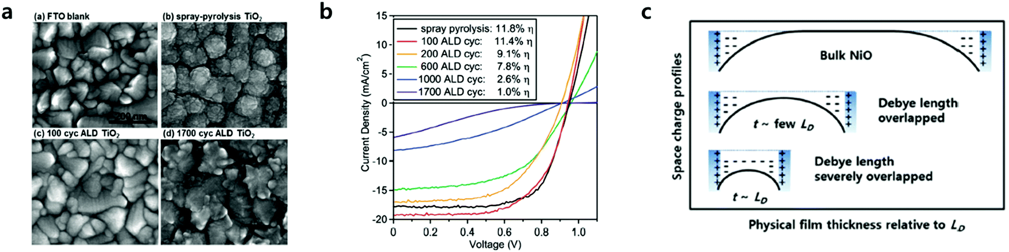 | ||
| Fig. 3 (a) SEM images of TiO2 films grown on FTO, all at the same magnification with a 200 nm scale bar. (b) Performance of representative mesoporous perovskite solar cells with 50 nm thick spray-pyrolysis compact TiO2 layers, compared to varied thicknesses of ALD TiO2 from 100 ALD cycles (4 nm thick) to 1700 ALD cycles (90 nm thick). Plotted are the settled J–V performance under 1 sun of AM 1.5 illumination. Reproduced with permission.43 Copyright 2016, Wiley-VCH. (c) Schematic images of physical films’ thickness relative to the Debye length (LD) vs. space charge profiles. When the thickness of NiO films is large enough compared to the LD, the NiO films were bulk-like, thus insulating ones as shown in the inset (top). Once the films' thicknesses were thin enough, the LD started to overlap, and thus the apparent work function and hole concentration are increased (schematic in middle). Even in thinner films, LD is severely overlapped (schematic in the bottom). Reproduced with permission.40 Copyright 2016, The Royal Society of Chemistry. | ||
| Material | Precursor | T substrate (°C) | Device configurationa | Device structure | V oc (V) | J sc (mA cm−2) | FF (%) | PCE (%) | Ref. |
|---|---|---|---|---|---|---|---|---|---|
| a Device configurations are categorized into nip (regular n–i–p), P (planar heterojunction), M (mesoscopic), F (Flexible), and pin (inverted p–i–n). | |||||||||
| TiO2 | TDMAT + O2 plasma | 150 | nip(P)F | ITO/ALD TiO2/MAPbI3−xClx/Spiro-OMeTAD/Au | 0.88 | 14.9 | 0.7 | 9.2 | 45 |
| TDMAT + H2O | 80 | nip(M) | FTO/ALD TiO2 nanostructures/CH3NH3PbI3−xClx/P3HT/Ag | 0.92 | 21.5 | 60.3 | 12.5 | 46 | |
| TDMAT + H2O | 80 | nio(P) | FTO/ALD TiO2/CH3NH3PbI3−xClx/P3HT/Ag | 0.98 | 24.3 | 57.1 | 13.6 | 44 | |
| TDMAT + H2O | 150 | nip(M) | FTO/m-TiO2/ALD TiO2/MAPbI3/Spiro-OMeTAD/Ag | 1.07 | 20.5 | 75.2 | 16.5 | 42 | |
| TDMAT + H2O | 200 | nip(M) | FTO/ALD TiO2/m-TiO2/perovskite/Spiro-OMeTAD/Au | 0.93 | 18.7 | 72.0 | 12.6 | 43 | |
| TDMAT + H2O | 120 | nip(P) | FTO/ALD asdep TiO2/MAPbI3−xClx/Spiro-PMeTAD/Au | 0.82 | 10.0 | 21.8 | 1.8 | 47 | |
| 120 | nip(P) | FTO/ALD UV_O3 TiO2/MAPbI3−xClx/Spiro-PMeTAD/Au | 0.86 | 25.6 | 45.2 | 10.0 | |||
| 120 | nip(P) | FTO/ALD 500 °C ann TiO2/MAPbI3−xClx/Spiro-PMeTAD/Au | 0.96 | 26.7 | 44.3 | 11.5 | |||
| Ti(CpMe)(NMe2)3 + O2 plasma | 150 | nip(M)F | PET/ITO/ALD TiO2/m-TiO2/CH3NH3PbI3/Spiro-OMeTAD/Au | 1.03 | 17.0 | 75.2 | 13.5 | 41 | |
| Ti(CpMe)(NMe2)3 + O2 plasma | 150 | nip(P)F | PET/ITO/ALD TiO2/m-TiO2/CH3NH3PbI3/Spiro-OMeTAD/Au | 0.86 | 12.1 | 71.9 | 7.5 | 48 | |
| — | nip(M)F | PET/ITO/ALD TiO2/CH3NH3PbI3/Spiro-OMeTAD/Au | 0.91 | 2.9 | 46.7 | 1.3 | |||
| TiCl4 + H2O | — | nip(P) | FTO/ALD TiO2/MAPbI3/Spiro-OMeTAD/Au | 1.01 | 16.4 | 59.5 | 9.9 | 40 | |
| TiCl4 + H2O | 300 | nip(M) | FTO/ALD TiO2/m-TiO2/MAPbI3/Spiro-OMeTAD/Ag | 1.02 | 21.0 | 71.9 | 15.4 | 49 | |
| TiCl4 + H2O | 100 | nip(M) | FTO/ALD TiO2/m-TiO2/MAPbI3/Spiro-OMeTAD/Au | 0.97 | 22 | 68.0 | 11.5 | 38 | |
| TTIP + O2 Plasma | 80 | nip(P)F | PEN/ITO/CH3NH3PbI3−xClx/Spiro-OMeTAD/Ag | 0.95 | 21.4 | 60.0 | 12.2 | 50 | |
| TTIP + O2 Plasma | 130 | nio(P) | ITO/ALD TiO2/MAPbI3/Spiro-OmeTAD/Au | 1.03 | 20.3 | 75.5 | 15.8 | 51 | |
| TTIP + H2O | 150 | nip(M) | FTO/ALD TiO2/m-TiO2/MAPbI3/carbon | 0.96 | 19.5 | 41.5 | 7.8 | 52 | |
| SnO2 | TDMASn + Ozone | 100 | nip(P) | FTO/c-TiO2/ALD SnO2/(FAPbI3)0.85(MAPbBr3)0.15/PTAA/Au | 1.13 | 22.7 | 78.0 | 20.0 | 53 |
| TDMASn + Ozone | 118 | nip(P) | FTO/ALD SnO2/Rb1(MA0.17FA0.83)99Pb(I0.83Br0.17)3/Spiro-OMeTAD/Au | 1.17 | 23.1 | 74.0 | 20.3 | 54 | |
| TDMASn + Ozone | 118 | nip(P) | FTO/ALD SnO2/mixed perovskite/Spiro-OMeTAD/Au | 1.17 | 23.0 | 71.0 | 20.0 | 55 | |
| TDMASn + Ozone | 118 | nip(P) | FTO/ALD SnO2/(FAPbI3)0.85(MAPbBr3)0.15/Spiro-OMeTAD/Au | 1.14 | 21.3 | 74.0 | 18.4 | 56 | |
| TDMASn + O2 plasma | 100 | nip(P) | FTO/ALD-SnO2/C60-SAM/MAPbI3/Spiro-OMeTAD/Au | 1.07 | 20.7 | 70.3 | 15.6 | 57 | |
| TDMASn + O2 plasma | 200 | nip(P) | ITO/ALD SnO2/Cs0.05(MA0.17FA0.83)0.95PbI2.7Br0.3/Spiro-OMeTAD/Au | 1.08 | 22.1 | 75.0 | 17.8 | 58 | |
| TDMASn + O2 plasma | 100 | nip(P)F | PET/ITO/ALD SnO2/C60-SAM/perovskite/Spiro-OMeTAD/Au | 1.10 | 22.1 | 75.4 | 18.4 | 59 | |
| TDMASn + O2 plasma | — | nip(P) | FTO/ALD SnO2/MA0.7FA0.3PbI3/Spiro-OMeTAD/Au | 1.12 | 22.3 | 78.8 | 19.6 | 60 | |
| ZnO | ZnEt2 + H2O | 70 | nip(P) | FTO/450 °C sintered ALD ZnO/MAPbI3/Spiro-OMeTAD/Ag | 0.88 | 11.4 | 59.0 | 6.0 | 61 |
| ZnEt2 + H2O | 70 | nip(P) | FTO/ALD ZnO/MAPbI3/Spiro-OMeTAD/Ag | 0.80 | 7.4 | 51.0 | 3.0 | ||
| Nb2O5 | TBTDEN + ozone | 130 | nip(P) | FTO/ALD Nb2O5/(FAPbI3)0.85(MAPbBr3)0.15/Spiro-OMeTAD/Au | Very low | 56 | |||
| NiO | MABONi + ozone | 200 | pin(P) | ITO/ALD NiO/MAPbI3/PCBM/Ag | 1.04 | 21.9 | 72.0 | 16.4 | 35 |
| TiO2–IrOx | TDMAT/((EtCp)Ir(CHD)) + ozone | 175 | pin(P) | ITO/ALD TiO2–IrOx/Cs0.17FA0.83Pb(I0.83Br0.17)3/C60/BCP/Ag | 1.01 | 19.6 | 80.0 | 15.8 | 62 |
The initial ALD ETL study on underlying ETLs based on TiO2 focused on the clarification of the superiority of the ALD process compared to other solution-processes, i.e., mostly sol–gel spin coating and spray-pyrolysis.43,45–48 Lu et al. fabricated pinhole-free and compact ETL TiO2 films processed by ALD for planar n–i–p PSCs as shown in Fig. 4a.49 ALD TiO2 showed a better PCE of 13.6% compared to that of solution-processed TiO2 (i.e., 8.7%). They have figured out that the optimum thickness of ALD TiO2 is 10 nm where PSCs exhibit the best performance. PSCs with ultra-thin ALD TiO2 films (5–20 nm) showed better photocurrent compared to those with solution-based TiO2, thanks to the excellent transmittance in the wavelength range of 400–900 nm. They also found that the ALD TiO2/perovskite interface generates less leakage current, due to the dense and pinhole-free film quality provided by ALD.
 | ||
| Fig. 4 (a) Cross-sectional SEM image of a perovskite solar cell with FTO/ALD TiO2/perovskite/P3HT/Ag layers and J–V curves of solar cells based on conventional TiO2 and ALD TiO2 layers (5, 10, 15 and 20 nm). Reproduced with permission.49 Copyright 2015, The Royal Society of Chemistry. (b) J–V curves of the perovskite solar cells with ALD TiO2 as the ETL (solid black line) and CF4 plasma-treated ALD (dash red line); and maximum power point tracking (MPPT) for the two devices. Reproduced with permission.52 Copyright 2018, Wiley-VCH. | ||
Lu et al. have subsequently proposed that the conduction band edge and Fermi level of ALD TiO2 has been slightly shifted shallower relative to that of solution-processed TiO2 due to the higher concentrations of Ti3+ defects and surface absorbed –OH groups in the film, evidenced by X-ray photoelectron spectroscopy (XPS).47 Utilizing these energy level differences, they formed a solution-based TiO2/ALD TiO2 bilayer ETL with type II band alignment and recorded a PCE of up to 16.5%. In spite of demonstrations of the superiority of the ALD process, it hardly obtained highly efficient planar PSCs based on TiO2, noted by the poor interface between the TiO2/perovskite regardless of the processes.50 It has been proposed that interfacial modification,13 or the doping51 strategy of solution-processed TiO2 could improve the performance of planar PSCs. Zardetto et al. reported that the interfacial property between the ALD TiO2/perovskite can be improved by the surface treatment of CF4 gas under plasma.52 CF4-treated TiO2 has a deeper energy level compared to the pristine one, which allows better formation of the band alignment with the perovskite layer and facilitates electron extraction. In addition, the surface of CF4-treated TiO2 improved the interfacial adhesion when perovskite-coated, increasing the maximum PCE up to 14.8% from 4% (Fig. 4b).
The application of ALD SnO2 layers in planar PSCs was more successful than ALD TiO2 ones in terms of their PV performances. Correa et al. firstly reported that the planar PSC based on ALD SnO2, deposited at a low temperature of 118 °C, recorded a maximum PCE of 18.4%.53 They observed that ALD SnO2 forms barrier-free band alignment with mixed cations halides perovskite layers ((FAPbI3)0.85(MAPbBr3)0.15). Furthermore, an efficient extraction of the electrons from the perovskite into SnO2 was proven by femtosecond transient absorption (TA) measurement. Consequently, PSCs with ALD SnO2 show no current–voltage hysteresis or reproducible current–voltage characteristics regardless of scan rates (Fig. 5a). The importance of band alignment between ETL/perovskite in planar PSCs was well highlighted. In their later study, SnO2 was passivated by thin (<1 nm) Ga2O3 interlayers for the sake of the suppression of interfacial recombination.54 However, the passivation of Ga2O3 did not show any improvement in PV performances. In addition, they have confirmed that interfacial recombination near SnO2 is considerably well suppressed by the intrinsic interfaces between the ALD SnO2/perovskite layers. Based on this ALD layer, which is energetically favourable with the perovskite, they reported that the incorporation of RbI into the MAFA-based perovskite can enhance the lifetime of charge carriers up to 1.37 μs (0.55 μs for non RbI-perovskites) and promote hysteresis-less current–voltage characteristics, eventually yielding a PCE of 20.3% (Fig. 5c).13 Furthermore, It was demonstrated that the Voc of the device could be enhanced to 1.23 V (just 100 mV lower than the thermodynamic limit) through the control of the doping level of HTL (Spiro-OMeTAD).14
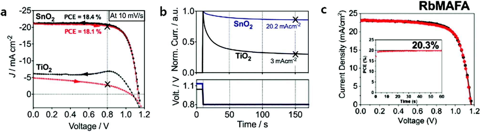 | ||
| Fig. 5 (a) Current–voltage properties of TiO2 and SnO2-based planar mixed halide/cation perovskite devices. Black arrows indicate the backward scan from Voc to Jsc, and red arrows indicate the reverse scan. (b) Normalized transient photocurrents measured from the Voc to the maximum power point voltage for both planar systems. Reproduced with permission.53 Copyright 2015, The Royal Society of Chemistry. (c) The performance of planar PSCs with 1% of Rb in MAFA showed the highest PCE of 20.3%. Reproduced with permission.13 Copyright 2018, The Royal Society of Chemistry. | ||
It is well known that the material properties of a semiconductor can typically be improved through high-temperature-induced recrystallization. In contrast, Lee et al. reported high-temperature (300 °C) annealed SnO2 layers largely decreased the performance of PSCs, while annealed SnO2 ones at mild temperatures (180 °C) showed better PV performances (Fig. 6).55 This trend has been consistently observed in PSCs not only with ALD SnO2 layers but also in other solution-processed SnO2 layers.56,57 They suggest that residual precursors, tetrakis(dimethylamino)tin (TDMASn) in case of the ALD process, in the SnO2 films decompose at high temperatures of 230 °C, leaving highly conductive SnO2 layers. The contrasting behavior of annealed SnO2 layers is ascribed to the reduction of the hole-blocking ability due to metal-like nature of SnO2. As a result, they were addressed as-deposited and mildly annealed SnO2 films containing self-passivating residual precursors, which is inevitably required to provide good electron mobility as well as hole-blocking property.
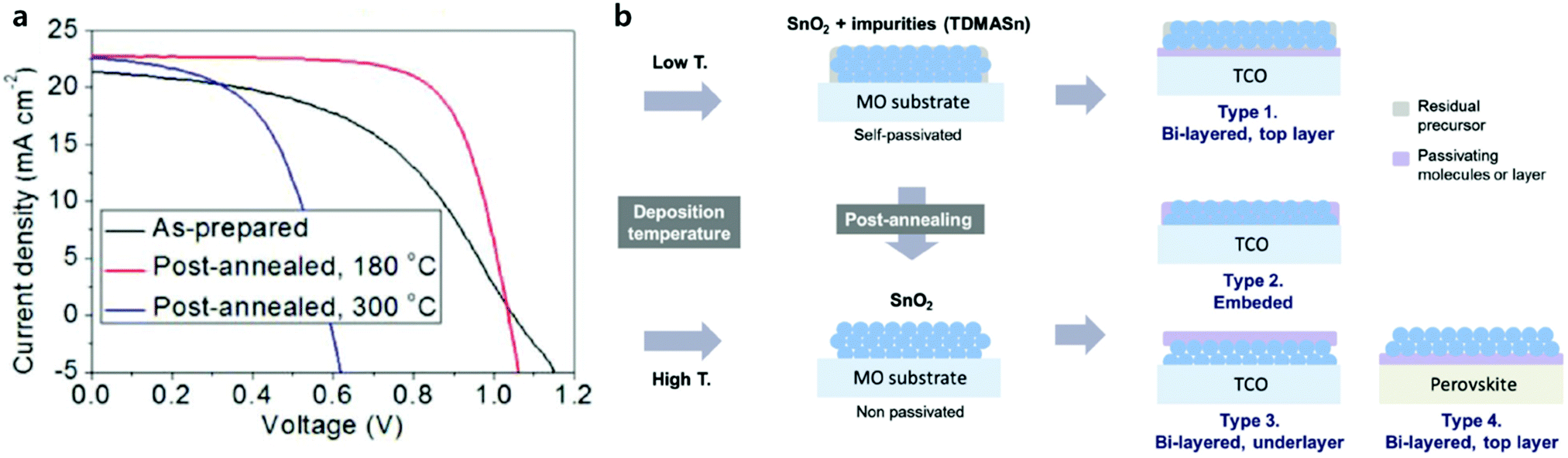 | ||
| Fig. 6 (a) J–V curve change according to the post-annealing of ALD SnO2 films. (b) Self- and post-passivation of the ALD SnO2 films. Low-temperature deposition results in incomplete conversion of the precursor, which remains on the SnO2 film as a self-passivating layer. The schematic shows that the surface passivation of SnO2 films can be controlled by post-annealing. Four different methods of post-passivation are proposed. Reproduced with permission.55 Copyright 2018, The Royal Society of Chemistry. | ||
Several SnO2via plasma-assisted ALD applied to planar PSCs has also been investigated.58–61 Wang et al. further reduced the process temperature of SnO2 to 70 °C thanks to the additional energy from plasma, which resulted in the maximum PCE of 19%.60 They utilized C60-SAM as an interfacial modifier on SnO2 to suppress the interfacial recombination. Considering its high electron mobility as well as its energy level position, SnO2 is one of the most suitable candidates in planar PSCs. Many researchers have considered doping strategies to obtain better electron transfer within SnO2 due to its wide band gap nature.62 However, it is not the desired process because the doping process also frequently requires high-temperature annealing. Thus, SnO2via the ALD process, capable of sub-nanometer thickness control of the thin film, can exhibit most excellent properties as an ETL, which makes it possible to realize a high PCE of even above 20 or 21%.
The ambipolar carrier transport properties of the perovskites enabled structural versatility including p–i–n architecture. In the case of p–i–n PSCs, underlying inorganic HTL materials such as NiO, CuO, CuSCN, MoO3, and Cu-based delafossite were applied to the PSCs.63 The most investigated inorganic HTL in p–i–n PSCs is NiO, which requires surface modification, nanostructuring, or doping to minimize its intrinsically high resistances. Seo et al. reported the first un-doped pure NiO ultra-thin film via ALD in p–i–n PSCs with a PCE of 16.4%.40 They optimized the thickness of ALD NiO (7.5 nm) and exhibited the appropriated work function of 5.0–5.2 eV and high transmittance of above 95% in the visible range. Tan et al. proposed that conventional electron transporting material TiO2 can be a good hole transporting material by the incorporation of IrOx (TiO2–IrOx composition via super-cycle ALD).64 This ALD layer has a work function of 5.2 eV and p-type semiconducting property. When 15.5 mol% of IrOx is incorporated into the TiO2 film, it shows suitable HTL characteristics and a PCE of up to 15.8% at maximum. Several film deposition recipes via ALD chemistry were already developed for highly hole conductive CuO, CuCrO2 delafossite, and MoO3, which remained to be demonstrated as highly efficient p–i–n PSCs with these ALD layers.
ETL processed by ALD especially has superiority when applied to tandem or flexible devices requiring low-temperature processes, conformal and pinhole-free films. Albrecht et al. realized monolithic Si/perovskite tandem devices via low-temperature (118 °C) ALD-processed SnO2 layers (Fig. 7a).65 They formed a recombination layer of ITO/ALD SnO2 onto the flat Si sub-cell, which functions as an energetically aligned ETL with the perovskite. The ALD ETL in the tandem device is expected to become even more important due to its superior conformality when the Si bottom cell has a textured surface to manage more illuminated light. In the case of flexible devices, ALD TiO2 and SnO2 layers as CTLs were investigated.49,59,66,67 It is possible to deposit high-quality ETL by ALD at low temperatures (<150 °C), which is required in flexible substrates. It has been also reported that the uniform films without pinholes via ALD are more durable against cracks during device bending tests. Wang et al. recorded one of the highest PCE (18.36% in the reverse scan direction and a stabilized power output of over 17%) using ALD SnO2 among all n–i–p flexible PSCs.59 SnO2via plasma-assisted ALD with post-annealing under the water vapour (the entire process at a temperature below 100 °C) showed improved charge transport ability and electrical conductivity. They evidenced that this ALD layer on flexible substrates can alleviate the problems of lower Voc, FF and severe current–voltage hysteresis, compared to on rigid substrates. The flexible device retained 76% its initial PCE from 17.4 to 13.3% after 1000 bending cycles (Fig. 7b). They argued that the degradation of flexible ITO/polyethyleneterephthalate (PET) substrates with bending cycles is the predominant reason for the increased sheet resistance and decreased FF and PCE.68,69
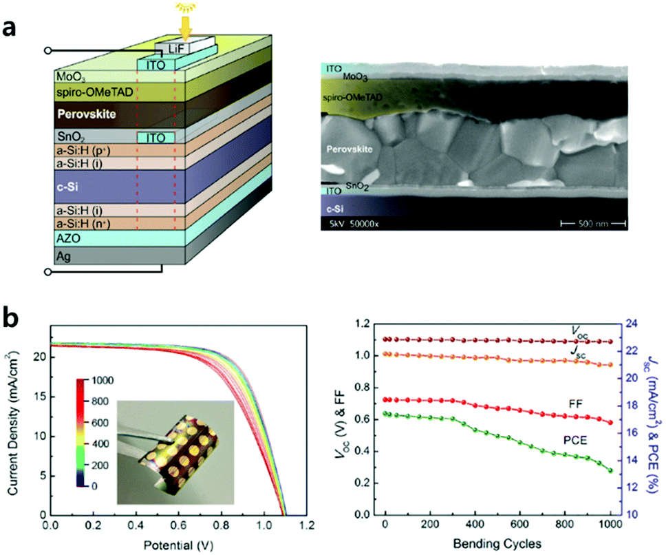 | ||
| Fig. 7 (a) Schematic of the Si heterojunction/perovskite tandem solar cell (the red dashed line indicates the active area) and cross-sectional scanning electron micrograph of a typical monolithic tandem solar cell. Reproduced with permission.65 Copyright 2016, The Royal Society of Chemistry. (b) Fatigue testing of a flexible PSC with a bending radius of 1 cm. J–V curves measured after various bending cycles and performance parameters as a function of bending cycles. Reproduced with permission.59 Copyright 2017, American Chemical Society. | ||
Another consideration in developing underlying CTLs is the different electronic properties (for example, VB, CB, and work function, etc.) of the perovskite films depending on their CTLs, which was reported by several research groups.70–73 They found that the work function of perovskite films was determined to be around 4.0 eV on n-type substrates (i.e., TiO2, SnO2) while the films were around 4.7 eV for the work function on p-type substrates (i.e., NiO, PEDOT:PSS). Olthof et al. proposed that OH– surface groups on oxide materials, by-product formations including the unreacted PbI2 at the surfaces during the film growth, and the interface dipole could be the origin of the different electronic properties of the perovskite films.71 Hu et al. reported a strong impact on the device performance by different SnO2 variants prepared from ALD with three different oxidizers (i.e., H2O, ozone, and plasma-treatment).70 The device based on ozone SnO2 showed the highest efficiency and Voc of 1.17 V with negligible hysteresis. They asserted that the CB mismatch between the MAPbI3 and the unreacted PbI2 on SnO2 was caused by different interfacial dipoles depending on SnO2 films grown by different oxidizers and surface treatment. A clear understanding of the CTL/perovskite interfaces is still lacking thus far. However, it can be progressed further in the design of efficient PSCs with the understanding of the chemical reactions resulting in the formation of desirable interfaces. For example, the elimination of interfacial PbI2 or control of the interfacial dipole would be viable options to be considered.
2.2 Surface passivation/interface engineering
Since the defects and impurities present on the surfaces of the semiconductor promote the electron–hole recombination, interfacial properties of the solar cells are particularly important for highly efficient PVs. Interfaces between the CTLs and perovskite layers are the main source of charge recombination in PSCs.74 Surface passivation introduced by ultra-thin layers at relatively low temperatures of deposition should cover the surfaces to minimize thermally induced pinholes or cracks in the layers. Thin insulating tunnel layers can also act as a passivation layer by reducing interfacial recombination and charge transfer via tunnelling.ALD provides ideal uniform and conformal passivation films of high quality at a relatively low temperature, which have already been widely adopted as a passivation layer in other solar cell fabrication processes.75 Chandiran et al. proposed the nanometer-thickness ALD TiO2 overlayers (0–4 nm) on mesoporous TiO2-based PSCs to suppress electron recombination, leading to a PCE of 11.5% without further heat treatment.76 Similar concepts of ALD metal oxide passivation films with the thickness of few nanometres have been employed in various configurations (ALD ZnO on mesoporous Al2O3,77 ALD Al2O3 between FTO/mesoporous TiO2,78 ALD TiO2 on 1-D nanorod TiO2,79etc.76,80,81).
The passivation process on the TCO electrodes or TCO/metal oxide substrates before perovskite coating is more challenging and limited than the passivation process on top of the perovskite or perovskite/CTLs in terms of compatibility without having any damage underneath the perovskite layers, prone to degradation, during the process.82 However, when the passivation process over the perovskite is performed successfully, the passivation layer can not only reduce charge recombination at the interface but also improve the stability of the perovskite by protecting the degradation reaction with moisture and/or oxygen from outside of the cells. Dong et al. investigated ultrathin Al2O3 prepared by ALD on the perovskite layer as a passivation process.83 They deposited Al2O3 directly onto the perovskite using TMA and O3 with a relatively low temperature of 70 °C to avoid the thermally induced degradation of the perovskite and organic HTL. The perovskite was degraded even after 1 cycle of the ALD process, which resulted in the reduced performance of the PSCs. Even though they reported the successful enhancement of stability by adopting the Al2O3 layer, they did not explain the passivation tunnelling effect of ALD Al2O3 due to the performance drop. Kim et al. proposed novel ALD chemistry of the non-hydrolytic process using carboxyl acid as an oxidizer for Al2O3 deposition to avoid perovskite degradation.84 They were not successful in showing PSCs adopting the non-hydrolytic ALD process, due to which the passivation effect of the film remains unclarified.
Recently, Koushik et al. deposited 2–20 cycles of ALD Al2O3 onto the perovskite at room temperature without degradation, evidenced by the X-ray diffraction (XRD) spectra as shown in Fig. 8.85 The thickness of the Al2O3 films was grown conformally and precisely controlled at the Angstrom scale by varying the number of ALD cycles. Devices without Al2O3 layers exhibited a PCE of 15.1%. Device passivated by Al2O3 showed considerable improvement in all PV performances with sub-optimal conditions (2–8 cycles) and optimal conditions (10–15 cycles). Further increasing the number of ALD cycles over 15 resulted in a significant decrease in the Jsc and FF. The author addressed that the relatively thick Al2O3 worsened the tunnelling effect, followed by less probable hole injection from the perovskite to the HTL. ALD Al2O3 layers with an optimal thickness (10 cycles ∼1 nm) positively affected current–voltage hysteresis and increased the PCE of PSCs up to 18%, which provided sufficient tunnelling passivation effect and protected the underneath perovskite layers. 70 days of dark aging under a stepwise increasing humidity (RH 40% to 70%) demonstrated that the Al2O3 passivation layers delay humidity-induced degradation, as it retained 70% of its initial efficiency, while devices without the Al2O3 layers lost almost all highly efficient PV performance.
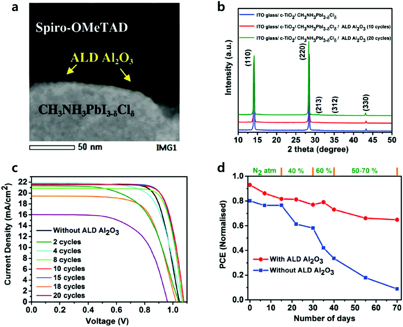 | ||
| Fig. 8 (a) High-angle annular dark field (HAADF) scanning TEM image of the enlarged perovskite/ALD Al2O3/Spiro-OMeTAD interface. (b) XRD spectra of the parent perovskite film before and after the successive depositions of ALD Al2O3. (c) J–V curves of the best perovskite devices utilizing different numbers of ALD Al2O3 cycles. (d) Normalized PCE of the champion perovskite devices with and without ALD Al2O3 as a function of storage time under varied humidity conditions. Reproduced with permission.85 Copyright 2017, The Royal Society of Chemistry. | ||
Hu et al. reported another passivation material, i.e., ALD ZrO2 to modify the interface between perovskite/PCBM in MAPbBr3-based inverted planar PSCs.86 Hole blocking by ZrO2 suppresses charge recombination loss and consequently produces a remarkably high Voc of 1653 mV. The author additionally addressed the origin of Voc enhancement of ZrO2-inserted PSCs, since the arrangement of PCBM films is more ordered on the perovskite/ZrO2 surface, as evidenced by XRD analysis.
2.3 Overlying ETL via ALD for stability engineering
The stability of PSCs for the goal of commercially available products is one of the most difficult challenges in PSCs. The prototypical light absorbing material in PSCs is CH3NH3PbI3, which has ABX3 perovskite crystal structure, and it has a relatively low lattice formation energy of −29.71 eV per cell, as much as 1-order of magnitude lower than typical oxide perovskites, resulting in facile degradation under moisture, oxygen, heat, electrical bias, as well as from light illumination.87 It has been proposed that alternating or mixing the A-site elements of MA with formamidinium (FA), Cs, Rb or even bigger organic cations to enhance the lattice formation energy can stabilize the perovskite structure and eventually increased the stability of the devices.Asghar et al. reviewed the understanding of the degradation mechanisms of PSCs originated from all the device components from the perovskite, transport layers, electrodes, and device geometry.88 Not to mention the stability of the perovskite material itself, other components can promote or retard the degradation of PSCs. The components on top of the perovskite are of particular interest due to the additional protecting role preventing the penetration of moisture from the outside and its own stability. The conventional HTL in regular-type PSCs is the Spiro-OMeTAD, PTAA and poly(3-hexylthiophene) (P3HT), which is solution-processed. Yang et al. studied the ability of HTL to prevent moisture-induced degradation onto the perovskite.89 They found that Spiro-OMeTAD causes an acceleration of the decomposition of the perovskite due to the HTL undergoing significant cracking, while other HTLs show a reduction in the degradation rates. They explained the different rates of perovskite decomposition by the toughness of the layer. PCBM, the most common ETL in inverted devices, has been reported to inhibit water permeation due to its hydrophobic nature.90 Thus, this is the reason why layers over the perovskite should be dense, impermeable and free of pinholes in terms of stability.
ALD has been proposed as a promising method to produce an excellent protective layer when deposited onto the perovskite layer.84 Metal oxide films were grown via ALD with great impermeability originating from dense, conformal, and pinhole-free nature with an extremely low water vapour transmission rate (WVTR).91 The first application of ALD for stable PSCs was reported by depositing a few cycles of Al2O3 directly onto the perovskite layer as introduced in the previous passivation section.92
In spite of its sub-nanometer thickness, it has improved the atmospheric air stability of PSCs. The trade-off between stability and charge transfer occurs simply because the thick film demonstrated sufficient impermeability, while charge transfer via tunnelling is severely suppressed. In order to avoid this problem, the deposition of 10–20 nm of ALD ETLs onto the perovskite-PCBM heterojunction has been proposed. ALD ETLs functions as a protective layer as well as CTLs in the inverted p–i–n type PSCs. Table 2 shows important stability results based on ALD ETL adopted inverted PSCs reported in the literature.91,93–97 The direct deposition of an ALD ETL with a thickness over 10 nm onto the perovskite usually decomposes the perovskite vigorously during the process, which make the final PCE less than 10%.98,99
| ALD metal oxide | Device structure | PCE (%) | Ageing condition and stability results | Ref. |
|---|---|---|---|---|
| ZnO | ITO/PEDOT:PSS/MAPbI3/PCBM/ALD ZnO/Ag NWs/50 nm Al2O3 coated PET | 10.8 | Dark storage in ambient air ∼95% retaining for 42 days | 87 |
| TiO2 | ITO/NiOx/MAPbI3/PCBM/ALD TiO2/Al/Au | 8.8 | Dark storage under thermal soaking (100 °C) 91% retaining for 10 hours | 88 |
| SnO2 | ITO/PEDOT:PSS/MAPbI3/PCBM/Al:ZnO/ALD SnO2/Ag | 12.6 | Dark storage in 23 °C and 50% RH or inert under 60 °C no degradation | 89 |
| SnO2 | ITO/PEDOT:PSS/MAPbI3/PCBM/Al:ZnO/ALD SnO2/Ag/SnO2 | 11.2 | Dark storage in inert 60 °C 95% retaining for 3200 hours | 90 |
| SnO2 | ITO/PEDOT:PSS/MAPbI3/PCBM/Al:ZnO/spatial ALD SnO2/Ag | 12.7 | Dark storage in 23 °C and 60% RH ∼92% retaining for 1000 hours | 91 |
| Al:ZnO | FTO/NiO/MAPbI3/PCBM/BCP/ALD-Al:ZnO/Ag/Al2O3(90 nm) | 18.5 | 85 °C, 1 sun illumination, ambient air, MPPT 86.7% retaining for 500 hours | 92 |
Kim et al. prepared TiO2 layers by ALD in the inverted PSCs, which showed remarkable improvement in resistance against degradation in harsh environments such as soaking in liquid water or high temperatures (100 °C).93 It has also been reported by Brinkmann et al. that 20 nm thick impermeable ALD-SnO2 ETLs can suppress the decomposition of the perovskite.94 PSCs with ALD-SnO2 preserved their performance (∼12%) during 500 hours of dark storage under humid atmospheric exposure (relative humidity (RH) of 50%) without any sign of degradation, while PSCs without the SnO2 layer degraded rapidly within 50 hours. They analysed the reason why SnO2-inserted PSCs showed strikingly high stability, as shown in Fig. 9. From the XRD data, they found no severe decomposition of the perovskite when exposed to moisture regardless of SnO2 deposition, which meant that the bulk of the perovskite remained unchanged. On the other hand, XPS results showed a notable degradation with increasing I3d5/2 binding peaks from AgI on the surface of devices without ALD SnO2. Similar XPS analysis of thermally aged (60 °C) samples showed consistent results that the ALD SnO2 layer successfully prevented the evaporation of volatile organic components (e.g., MAI). They claimed that outstandingly dense gas permeation barriers by ALD suppressed the out-diffusion of the decomposition products.
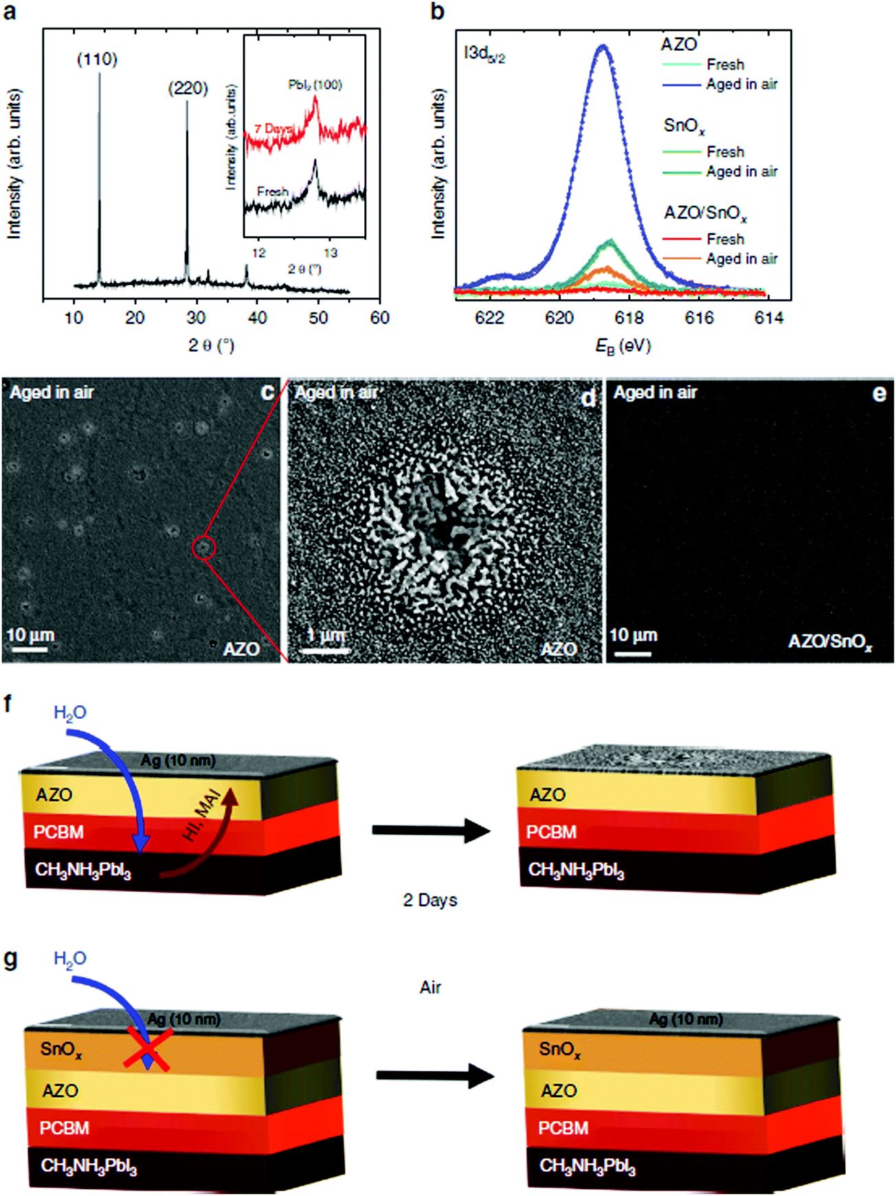 | ||
| Fig. 9 Unravelling the aging mechanism in air. XRD spectrum of a perovskite cell based on AZO as ETL after storage in air for 7 days (inset: magnified view of the (100) PbI2 reflection for a fresh sample and one that has been stored in air for 7 days; spectra were vertically offset for clarity) (a). Photoemission spectra of the iodine I3d5/2 peak for fresh and aged cells based on AZO, SnOx and bilayered AZO/SnOx ETLs, respectively (b). The aged samples were stored in air for 2 days. Corresponding plan-view SEM images of the 10 nm Ag layer in the case of the AZO sample (c and d), and for the AZO/SnOx sample (e). Schemes of the aging for the AZO and the AZO/SnOx samples (f and g). Reproduced with permission.94 Copyright 2016, Macmillan Publishers Limited. | ||
The moisture-induced degradation of PSCs can be overcome by proper encapsulation of the devices. Typical metal electrodes, such as Ag and Au, can diffuse through the organic transport layers and make detrimental reactions with the perovskite layers at the interface under operational condition or at high temperatures.100 Aforementioned ALD-grown inorganic CTLs are critical to prevent roles against in-/out-diffusion. Guerrero et al. reported the interfacial degradation of PSCs, as shown in Fig. 10a.101 PSCs under operational conditions including the light and electric field generate ion migration inside perovskite films, leaving the accumulation of net charges at one or both contacts. Light and electric field-driven chemical reaction by the diffusion of these ions and metals cause interfacial degradation between the perovskite/PCBM and the PCBM/metal, which finally induced a severe drop of the PCE even under inert atmosphere.
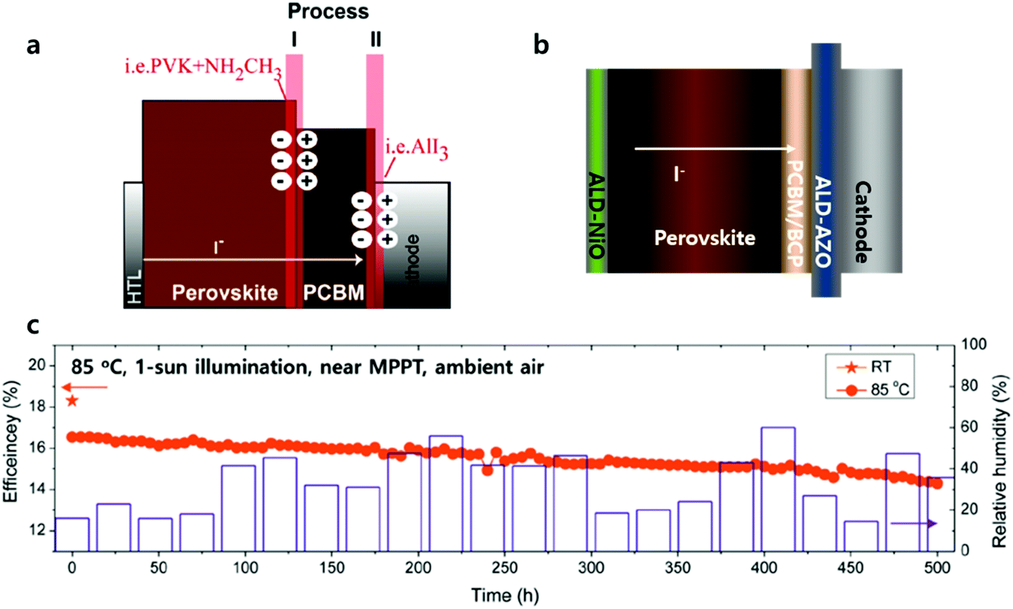 | ||
| Fig. 10 (a) Feasible hypothesis that could potentially give rise to external cathode contact degradation. Reproduced with permission.101 Copyright 2015, American Chemical Society. (b) Schematic of PSCs with suppressed interfacial degradation in the presence of the ALD Al:ZnO layer. (c) PCE evolution of the ALD-Al:ZnO-coated PSC with a thin Al2O3 passivation film (≈50 nm) over 500 h. Aging was performed under continuous near maximum power electrical biases (0.76–0.88 V) and 1 sun illumination (100 mW cm−2) with a 420 nm cutoff UV filter at 85 °C in ambient air (the relative humidity was ≈20–60%). The relative humidity was recorded every day. The initial PCE value (orange star) was 18.4% at room temperature, and the PCE at 85 °C (orange circles) was recorded every 5 h. The ALD-Al:ZnO-coated device retained 86.7% of its initial performance (16.5% → 14.3%), as determined from the reverse J–V scan. Reproduced with permission.97 Copyright 2018, Wiley-VCH. | ||
Seo et al. rationalized the use of the dense ALD-ETL layer between perovskite/PCBM and metal electrodes by suppressing interfacial degradation, as shown in Fig. 10b and c.97 They fabricated inverted PSCs using ALD Al:ZnO with FTO/NiO/perovskite/PCBM/Al:ZnO/Ag. Al:ZnO-adopted PSCs exhibited 17% efficiency, which produced similar device performance to the control device without Al:ZnO due to the negligible charge transporting retardation by the 3 orders of magnitude higher conductivity of Al:ZnO compared to that of PCBM. Regarding the stability of PSCs, while the control solar cells have been degraded rapidly under continuous 1 sun light illumination at room temperature in spite of the additional encapsulation layer (90 nm of Al2O3), Al:ZnO PSCs maintained almost all of its initial efficiency. The author addressed that the unique role of Al:ZnO, distinguished from other encapsulation techniques, is to prevent moisture penetration as well as interdiffusion at the perovskite/Ag interface when illuminated. The Al:ZnO layer prevents interfacial degradation between the perovskite-heterojunction and the Ag electrode caused by unfavourable chemical reaction. These perovskite solar cells demonstrated their stability in a harsher environment, exhibiting a power conversion efficiency of 18.45% and retaining 86.7% of its initial efficiency for 500 hours under continuous 1 sun illumination at 85 °C in ambient air with electrical biases (at the maximum power point). The application of the ALD ETL over the perovskite layer has another function of extending process compatibility to prevent deterioration of the perovskite during the deposition of transparent electrodes such as ITO. It was proposed by Bush et al. that sputtered ITO was successfully able to complete semi-transparent PSCs in the presence of ALD ETL due to its impermeability minimizing sputtered damage onto the perovskite.102 Moreover, Snaith and co-workers recently fabricated a solution-processed perovskite–perovskite tandem solar cell by utilizing ALD SnO2 as a buffer layer for the ITO sputtering process.102,103 The intermittent layer (SnO2/ITO) successfully protects underneath the perovskite during the top cell fabrication process.
2.4 Encapsulation via ALD
The key factor in achieving long-term stable PSCs is largely related to developing stable perovskite materials and/or device architectures including encapsulation. Encapsulation methods are utilized extensively in organic PVs (OPVs) or organic light emitting diodes (OLEDs), which requires levels of WVTR less than 10−6 g m−2 d−1 for long-lived OLEDs.104 However, encapsulation technology with adequate WVTR levels has not been developed yet in PSCs due to them being prone to the degradation of perovskite materials during the encapsulation processes.105,106Lee et al. reported the first laminated (inorganic and organic stacked layers) encapsulation thin film (thickness of less than 5 μm) for the encapsulation of PSCs, composed of pairs of Al2O3 and poly(1,3,5-trimethyl-1,3,5-trivinylcyclotrisiloxane) (pV3D3) processed by ALD and iCVD, respectively. Four pairs of Al2O3 and pV3D3 display an outstanding barrier property of 10−4 g m−2 d−1 of WVTR under a high RH of 90% and 38 °C.107Fig. 11 shows the effect of the ALD process temperature on the performance of the PSCs. In the case of PSCs with PTAA as the HTL, the performance retained 90% of its initial efficiency after the ALD process at 60 °C. One pair of Al2O3 and pV3D3 encapsulation films do not cause much deterioration of the performance, changing from 21.5 to 20.1%. PSCs with 4 pairs of encapsulation films maintained 97% of their initial PCE for 300 hours of ageing under 50 °C/50% (temperature/RH). The longest shelf life of PSCs, with an efficiency greater than 18%, has been achieved.
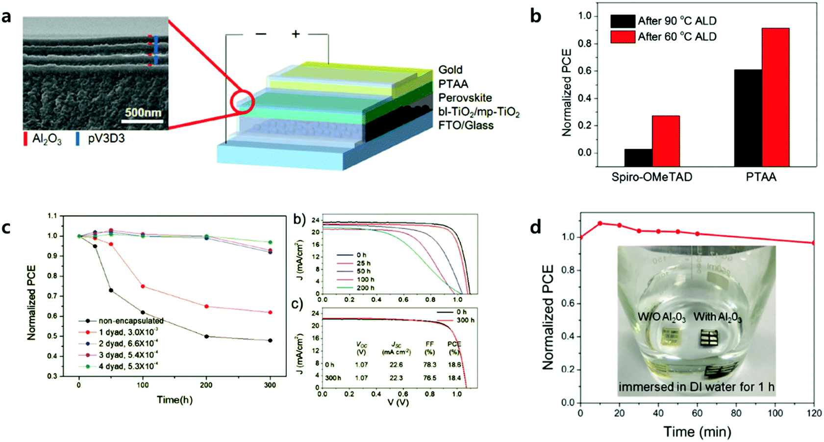 | ||
| Fig. 11 (a) Right: Schematic of the encapsulated PSC. Left: The cross-sectional SEM image of the TFE. (b) Normalized PCE of HTM-varied PSCs after 60 and 90 °C ALD processes. (c) Shelf life of PSC encapsulated with 1–4 layers of multilayer TFE under an accelerated condition of 50 °C, 50% RH. The numbers in legend indicate the WVTR of each TFE (g m−2 d−1). J–V characteristics of (b) pristine PSC and (c) PSC encapsulated with 4-dyad TFE with respect to time lapse under reverse scan. Reproduced with permission.107 Copyright 2017, Wiley-VCH. (d) Evolution of normalized PCE for Al2O3-protected devices immersed in water. The inset shows photographs of the devices with Al2O3 (right) and without Al2O3 (left) layers after being kept in water for 1 h. Reproduced with permission.109 Copyright 2018, American Chemical Society. | ||
Unlike regular PSCs, inverted PSCs usually showed better thermal stability due to the presence of PCBM instead of spiro-OMTeAD.91,108 The ALD Al2O3 process below 100 °C does not significantly affect the performance of inverted PSCs. Lv et al. reported a composite ALD Al2O3 encapsulation layer in multilayers composed of Al2O3 (10 nm)/Al2O3 with intermediates of the Al precursor (20 nm)/Al2O3 (30 nm) processed at 60 °C.109 PSCs with the Al2O3 multilayer showed great water resistance, retaining 95% of the initial efficiency after 2 hours of being immersed in DI water, as shown in Fig. 11d. Thin Al2O3 layers do not exhibit ideal water resistance at all. Water molecules might penetrate the layers from the surface of the Al2O3 up to the perovskite layers very slowly by forming H bonds with oxygens and migrating the species. They also proposed the novel concept of retarding water penetration. Intermediates of the Al precursor layer (O–Al–(CH3)3−x), between the top and bottom dense Al2O3 layers, additionally react with water. The intermediate layer can be converted into compact Al2O3 layers, which significantly decrease the overall water penetration rates as well as eliminating invading water molecules.
3. Conclusions
In this review, we mainly focused on underlying CTLs as well as overlying perovskite layers, surface passivation layers, and encapsulating layers all deposited by ALD in PSCs. A reduction of the thickness of CTLs can reduce the device serial resistance. Processing such ultra-thin films, however, has been challenging, and most thin film processing resulted in pinholes and cracks, leading to reduced charge carrier blocking ability and creating a shunt leakage pathway. Furthermore, in the case of large area substrates and/or substrates with a high-aspect ratio, the formation of ultra-thin films with uniform thicknesses is even more challenging. ALD can produce ideal CTLs with conformal and dense film growth with precise sub-nanometer scale thickness control. ETL processed by ALD has superiority when applied to tandem or flexible devices requiring low-temperature processes, conformal and pinhole-free films. ALD has also been widely adopted as a passivation layer in many different solar cell fabrication processes. Unlike passivation processed on the TCO electrodes or TCO/metal oxide substrates before perovskite coating, it is more challenging and limited than the passivation process atop of perovskite or perovskite/CTLs in terms of compatibility without having any damage underneath perovskite layers, prone to degradation. However, when the passivation process over the perovskite is performed successfully, the passivation layer can not only reduce charge recombination at the interface but also improve the stability by protecting the degradation reaction with moisture and/or oxygen from the outside. ALD has been proposed as a promising method to produce an excellent protective layer when deposited onto the perovskite layer. Metal oxide films grown via ALD, having great impermeability originating from a dense, conformal, and pinhole-free nature with extremely low water vapour transmission rate, can be a solution for the commercialization in PSCs.Further efficiency improvement can be expected in PSCs based on ALD CTLs by developing other potential candidate materials such as WO3, MoO3, V2O5, CuOx, doping strategies and interfacial engineering. Considering that many doping chemistries using ALD have already been reported, it would be an effective way to produce highly efficient CTLs. Until now, applications of doped CTLs via ALD for PSCs have rarely been reported. Furthermore, it is still unclear why perovskite layers exhibit different electronic properties depending on CTLs and their surface states. Since ALD can provide the same material with different surface properties using various oxidizers under similar growth conditions, it would be an ideal model system to understand the interfacial property between CTLs and perovskites.
The newly developed ALD ETL overlying perovskite has demonstrated huge potential for the stability improvement of PSCs. However, all these works have been directed towards inverted-type PSCs with MAPbI3. Thermally and chemically more stable perovskites containing Cs, FA, Rb, and/or Br will be able to explore the new possibility of the direct deposition of ETLs onto the perovskite layer without PCBM, which can reduce device serial resistance and complexity while preserving the efficiency of PSCs. Moreover, considering the overall efficiencies of regular-type PSCs, exhibiting higher PCEs compared to inverted-type PSCs, the development of ALD HTL overlying perovskite would be promising in terms of improving device stability as well as efficiency. Encapsulations via ALD Al2O3 for PSCs have been reported in the limited number of research papers to date. It is remarkable that negligible degradation in PV performance with encapsulation has been observed. It is also necessary to further reduce the WVTR of encapsulation layers for PSCs by benchmarking the excellent ALD encapsulation technology (e.g. ZrO2/Al2O3 bi-layer,110 organic/inorganic multilayer104) already developed in other fields. ALD techniques show great potential for efficient and stable PSCs and in the future will become the most viable ones in the fabrication of commercial PSCs.
Conflicts of interest
There are no conflicts to declare.Acknowledgements
The authors acknowledge the Ministry of Science, ICT & Future Planning (MSIP) of Korea under contracts with NRF-2017R1A4A1015770 (Basic Research Laboratory Program), NRF-2016M3D1A1027664 (Future Materials Discovery Program), NRF-2018K1A3A1A32055268 and NRF-2018M3C1B7021994 through the National Research Foundation of Korea (NRF).Notes and references
- A. Kojima, K. Teshima, Y. Shirai and T. Miyasaka, J. Am. Chem. Soc., 2009, 131, 6050 CrossRef CAS PubMed.
- J. H. Im, C. R. Lee, J. W. Lee, S. W. Park and N. G. Park, Nanoscale, 2011, 3, 4088 RSC.
- H. S. Kim, C. R. Lee, J. H. Im, K. B. Lee, T. Moehl, A. Marchioro, S. J. Moon, R. Humphry-Baker, J. H. Yum, J. E. Moser, M. Gratzel and N. G. Park, Sci. Rep., 2012, 2, 591 CrossRef PubMed.
- L. Etgar, P. Gao, Z. S. Xue, Q. Peng, A. K. Chandiran, B. Liu, M. K. Nazeeruddin and M. Gratzel, J. Am. Chem. Soc., 2012, 134, 17396 CrossRef CAS PubMed.
- M. M. Lee, J. Teuscher, T. Miyasaka, T. N. Murakami and H. J. Snaith, Science, 2012, 338, 643 CrossRef CAS PubMed.
- H. J. Snaith, J. Phys. Chem. Lett., 2013, 4, 3623 CrossRef CAS.
- Q. Q. Lin, A. Armin, P. L. Burn and P. Meredith, Acc. Chem. Res., 2016, 49, 545 CrossRef CAS PubMed.
- J. P. Correa-Baena, A. Abate, M. Saliba, W. Tress, T. J. Jacobsson, M. Gratzel and A. Hagfeldt, Energy Environ. Sci., 2017, 10, 710 RSC.
- J. S. Manser, J. A. Christians and P. V. Kamat, Chem. Rev., 2016, 116, 12956 CrossRef CAS PubMed.
- Y. X. Zhao and K. Zhu, Chem. Soc. Rev., 2016, 45, 655 RSC.
- M. A. Green and A. Ho-Baillie, ACS Energy Lett., 2017, 2, 822 CrossRef CAS.
- B. R.-C. National Renewable Energy Laboratory and E. c. https://www.nrel.gov/pv/assets/images/efficiency-chart.png.
- H. R. Tan, A. Jain, O. Voznyy, X. Z. Lan, F. P. G. de Arquer, J. Z. Fan, R. Quintero-Bermudez, M. J. Yuan, B. Zhang, Y. C. Zhao, F. J. Fan, P. C. Li, L. N. Quan, Y. B. Zhao, Z. H. Lu, Z. Y. Yang, S. Hoogland and E. H. Sargent, Science, 2017, 355, 722 CrossRef CAS PubMed.
- W. S. Yang, B. W. Park, E. H. Jung, N. J. Jeon, Y. C. Kim, D. U. Lee, S. S. Shin, J. Seo, E. K. Kim, J. H. Noh and S. I. Seok, Science, 2017, 356, 1376 CrossRef CAS PubMed.
- X. Zheng, B. Chen, J. Dai, Y. Fang, Y. Bai, Y. Lin, H. Wei, X. C. Zeng and J. Huang, Nat. Energy, 2017, 2, 17102 CrossRef CAS.
- D. Bi, C. Yi, J. Luo, J.-D. Décoppet, F. Zhang, S. M. Zakeeruddin, X. Li, A. Hagfeldt and M. Grätzel, Nat. Energy, 2016, 1, 16142 CrossRef CAS.
- Q. Jiang, Z. Chu, P. Wang, X. Yang, H. Liu, Y. Wang, Z. Yin, J. Wu, X. Zhang and J. You, Adv. Mater., 2017, 29, 1703852 CrossRef PubMed.
- Z.-L. Tseng, C.-H. Chiang, S.-H. Chang and C.-G. Wu, Nano Energy, 2016, 28, 311 CrossRef CAS.
- S. S. Shin, W. S. Yang, J. H. Noh, J. H. Suk, N. J. Jeon, J. H. Park, J. S. Kim, W. M. Seong and S. I. Seok, Nat. Commun., 2015, 6, 7410 CrossRef CAS PubMed.
- S. S. Shin, E. J. Yeom, W. S. Yang, S. Hur, M. G. Kim, J. Im, J. Seo, J. H. Noh and S. I. Seok, Science, 2017, 356, 167 CrossRef CAS PubMed.
- W. Chen, Y. Wu, Y. Yue, J. Liu, W. Zhang, X. Yang, H. Chen, E. Bi, I. Ashraful, M. Grätzel and L. Han, Science, 2015, 350, 944 CrossRef CAS PubMed.
- C. Zuo and L. Ding, Small, 2015, 11, 5528 CrossRef CAS PubMed.
- S. Ye, H. Rao, Z. Zhao, L. Zhang, H. Bao, W. Sun, Y. Li, F. Gu, J. Wang, Z. Liu, Z. Bian and C. Huang, J. Am. Chem. Soc., 2017, 139, 7504 CrossRef CAS PubMed.
- P.-L. Qin, H.-W. Lei, X.-L. Zheng, Q. Liu, H. Tao, G. Yang, W.-J. Ke, L.-B. Xiong, M.-C. Qin, X.-Z. Zhao and G.-J. Fang, Adv. Mater. Interfaces, 2016, 3, 1500799 CrossRef.
- H. Zhang, H. Wang, W. Chen and A. K.-Y. Jen, Adv. Mater., 2017, 29, 1604984 CrossRef PubMed.
- P.-L. Qin, Q. He, C. Chen, X.-L. Zheng, G. Yang, H. Tao, L.-B. Xiong, L. Xiong, G. Li and G.-J. Fang, Sol. RRL, 2017, 1, 1700058 CrossRef.
- H. Zhang, H. Wang, H. Zhu, C.-C. Chueh, W. Chen, S. Yang and A. K.-Y. Jen, Adv. Energy Mater., 2018, 8, 1702762 CrossRef.
- F. Hou, Z. Su, F. Jin, X. Yan, L. Wang, H. Zhao, J. Zhu, B. Chu and W. Li, Nanoscale, 2015, 7, 9427 RSC.
- K. M. Deng and L. Li, Adv. Mater. Interfaces, 2016, 3, 1600505 CrossRef.
- V. Zardetto, B. L. Williams, A. Perrotta, F. Di Giacomo, M. A. Verheijen, R. Andriessen, W. M. M. Kessels and M. Creatore, Sustainable Energy Fuels, 2017, 1, 30 RSC.
- R. L. Puurunen, Chem. Vap. Deposition, 2014, 20, 332 CrossRef CAS.
- V. Miikkulainen, M. Leskela, M. Ritala and R. L. Puurunen, J. Appl. Phys., 2013, 113, 021301 CrossRef.
- W. B. Niu, X. L. Li, S. K. Karuturi, D. W. Fam, H. J. Fan, S. Shrestha, L. H. Wong and A. L. Y. Tok, Nanotechnology, 2015, 26, 13 CrossRef PubMed.
- L. Ma, R. B. Nuwayhid, T. P. Wu, Y. Lei, K. Amine and J. Lu, Adv. Mater. Interfaces, 2016, 3, 1600564 CrossRef.
- Y. Widjaja and C. B. Musgrave, Appl. Phys. Lett., 2002, 80, 3304 CrossRef CAS.
- S. Lee, C. Bae and H. Shin, ACS Appl. Mater. Interfaces, 2018, 10, 20929 CrossRef CAS PubMed.
- S. Lee, C. Bae, J. Lee, S. Lee, S. H. Oh, J. Kim, G. S. Park, H. S. Jung and H. Shin, Adv. Mater., 2018, 30, 1706261 CrossRef PubMed.
- H. Shin, D. K. Jeong, J. Lee, M. M. Sung and J. Kim, Adv. Mater., 2004, 16, 1197 CrossRef CAS.
- M. D. Groner, F. H. Fabreguette, J. W. Elam and S. M. George, Chem. Mater., 2004, 16, 639 CrossRef CAS.
- S. Seo, I. J. Park, M. Kim, S. Lee, C. Bae, H. S. Jung, N. G. Park, J. Y. Kim and H. Shin, Nanoscale, 2016, 8, 11403 RSC.
- T. A. Ho, C. Bae, S. Lee, M. Kim, J. M. Montero-Moreno, J. H. Park and H. Shin, Chem. Mater., 2017, 29, 7604 CrossRef CAS.
- H. Nam, C. Bae and H. Shin, ChemistrySelect, 2018, 3, 11027 CrossRef.
- K. E. Roelofs, V. L. Pool, D. A. Bobb-Semple, A. F. Palmstrom, P. K. Santra, D. G. Van Campen, M. F. Toney and S. F. Bent, Adv. Mater. Interfaces, 2016, 3, 1600580 CrossRef.
- Y. Nosaka and A. Y. Nosaka, J. Phys. Chem. Lett., 2016, 7, 431 CrossRef CAS PubMed.
- L. Chen, J. R. Wang, L. Q. Xie, C. Zhan, Z. Qiu, J. Z. Zhou, J. W. Yan, B. W. Mao and Z. Q. Tian, Electrochem. Commun., 2016, 68, 40 CrossRef CAS.
- F. Di Giacomo, V. Zardetto, G. Lucarelli, L. Cina, A. Di Carlo, M. Creatore and T. M. Brown, Nano Energy, 2016, 30, 460 CrossRef CAS.
- H. Lu, W. Tian, B. K. Gu, Y. Y. Zhu and L. Li, Small, 2017, 13, 052301 Search PubMed.
- Y. Z. Wu, X. D. Yang, H. Chen, K. Zhang, C. J. Qin, J. Liu, W. Q. Peng, A. Islam, E. B. Bi, F. Ye, M. S. Yin, P. Zhang and L. Y. Han, Appl. Phys. Express, 2014, 7, 2130–2145 Search PubMed.
- H. Lu, Y. L. Ma, B. K. Gu, W. Tian and L. Li, J. Mater. Chem. A, 2015, 3, 16445 RSC.
- J. R. Lian, B. Lu, F. F. Niu, P. J. Zeng and X. W. Zhan, Small Methods, 2018, 2, 916–921 CrossRef.
- H. P. Zhou, Q. Chen, G. Li, S. Luo, T. B. Song, H. S. Duan, Z. R. Hong, J. B. You, Y. S. Liu and Y. Yang, Science, 2014, 345, 542 CrossRef CAS PubMed.
- V. Zardetto, F. di Giacomo, H. Lifka, M. A. Verheijen, C. H. L. Weijtens, L. E. Black, S. Veenstra, W. M. M. Kessels, R. Andriessen and M. Creatore, Adv. Mater. Interfaces, 2018, 5, 17999–18007 Search PubMed.
- J. P. C. Baena, L. Steier, W. Tress, M. Saliba, S. Neutzner, T. Matsui, F. Giordano, T. J. Jacobsson, A. R. S. Kandada, S. M. Zakeeruddin, A. Petrozza, A. Abate, M. K. Nazeeruddin, M. Gratzel and A. Hagfeldt, Energy Environ. Sci., 2015, 8, 2928 RSC.
- J. P. Correa-Baena, W. Tress, K. Domanski, E. H. Anaraki, S. H. Turren-Cruz, B. Roose, P. P. Boix, M. Gratzel, M. Saliba, A. Abate and A. Hagfeldt, Energy Environ. Sci., 2017, 10, 1207 RSC.
- Y. Lee, S. Lee, G. Seo, S. Paek, K. T. Cho, A. J. Huckaba, M. Calizzi, D. W. Choi, J. S. Park, D. Lee, H. J. Lee, A. M. Asiri and M. K. Nazeeruddin, Adv. Sci., 2018, 5, 1207–1212 Search PubMed.
- Y. Lee, S. Paek, K. T. Cho, E. Oveisi, P. Gao, S. Lee, J. S. Park, Y. Zhang, R. Humphry-Baker, A. M. Asiri and M. K. Nazeeruddin, J. Mater. Chem. A, 2017, 5, 12729 RSC.
- K. H. Jung, J. Y. Seo, S. Lee, H. Shin and N. G. Park, J. Mater. Chem. A, 2017, 5, 24790 RSC.
- Y. H. Kuang, V. Zardetto, R. van Gils, S. Karwal, D. Koushik, M. A. Verheijen, L. E. Black, C. Weijtens, S. Veenstra, R. Andriessen, W. M. M. Kessels and M. Creatore, ACS Appl. Mater. Interfaces, 2018, 10, 30367 CrossRef CAS PubMed.
- C. L. Wang, L. Guan, D. W. Zhao, Y. Yu, C. R. Grice, Z. N. Song, R. A. Awni, J. Chen, J. B. Wang, X. Z. Zhao and Y. F. Yan, ACS Energy Lett., 2017, 2, 2118 CrossRef CAS.
- C. L. Wang, D. W. Zhao, C. R. Grice, W. Q. Liao, Y. Yu, A. Cimaroli, N. Shrestha, P. J. Roland, J. Chen, Z. H. Yu, P. Liu, N. Cheng, R. J. Ellingson, X. Z. Zhao and Y. F. Yan, J. Mater. Chem. A, 2016, 4, 12080 RSC.
- C. L. Wang, C. X. Xiao, Y. Yu, D. W. Zhao, R. A. Awni, C. R. Grice, K. Ghimire, I. Constantinou, W. Q. Liao, A. J. Cimaroli, P. Liu, J. Chen, N. J. Podraza, C. S. Jiang, M. M. Al-Jassim, X. Z. Zhao and Y. F. Yan, Adv. Energy Mater., 2017, 7, 14405–14408 Search PubMed.
- L. B. Xiong, Y. X. Guo, J. Wen, H. R. Liu, G. Yang, P. L. Qin and G. J. Fang, Adv. Funct. Mater., 2018, 28, 1802757 CrossRef.
- J. Z. Chen and N. G. Park, J. Phys. Chem. C, 2018, 122, 14039 CrossRef CAS.
- W. L. Tan, O. L. Hendricks, A. C. Meng, M. R. Braun, M. D. McGehee, C. E. D. Chidsey and P. C. McIntyre, Adv. Mater. Interfaces, 2018, 5, 1800191 CrossRef.
- S. Albrecht, M. Saliba, J. P. C. Baena, F. Lang, L. Kegelmann, M. Mews, L. Steier, A. Abate, J. Rappich, L. Korte, R. Schlatmann, M. K. Nazeeruddin, A. Hagfeldt, M. Gratzel and B. Rech, Energy Environ. Sci., 2016, 9, 81 RSC.
- V. Zardetto, F. Di Giacomo, G. Lucarelli, W. M. M. Kessels, T. M. Brown and M. Creatore, Sol. Energy, 2017, 150, 447 CrossRef CAS.
- B. J. Kim, D. H. Kim, Y. Y. Lee, H. W. Shin, G. S. Han, J. S. Hong, K. Mahmood, T. K. Ahn, Y. C. Joo, K. S. Hong, N. G. Park, S. Lee and H. S. Jung, Energy Environ. Sci., 2015, 8, 916 RSC.
- J. H. Heo, M. H. Lee, H. J. Han, B. R. Patil, J. S. Yu and S. H. Im, J. Mater. Chem. A, 2016, 4, 1572 RSC.
- C. Zhang, D. W. Zhao, D. E. Gu, H. Kim, T. Ling, Y. K. R. Wu and L. J. Guo, Adv. Mater., 2014, 26, 5696 CrossRef CAS PubMed.
- T. Hu, T. Becker, N. Pourdavoud, J. Zhao, K. O. Brinkmann, R. Heiderhoff, T. Gahlmann, Z. Q. Huang, S. Olthof, K. Meerholz, D. Tobbens, B. C. Cheng, Y. W. Chen and T. Riedl, Adv. Mater., 2017, 29, 1606656 CrossRef PubMed.
- S. Olthof and K. Meerholz, Sci. Rep., 2017, 7, 40267 CrossRef CAS PubMed.
- T. Leijtens, S. D. Stranks, G. E. Eperon, R. Lindblad, E. M. J. Johansson, I. J. McPherson, H. Rensmo, J. M. Ball, M. M. Lee and H. J. Snaith, ACS Nano, 2014, 8, 7147 CrossRef CAS PubMed.
- P. Schulz, L. L. Whittaker-Brooks, B. A. MacLeod, D. C. Olson, Y. L. Loo and A. Kahn, Adv. Mater. Interfaces, 2015, 2, 1400532 CrossRef.
- Y. Yang, M. J. Yang, D. T. Moore, Y. Yan, E. M. Miller, K. Zhu and M. C. Beard, Nat. Energy, 2017, 2, 16207 CrossRef CAS.
- L. Y. Wen, M. Zhou, C. L. Wang, Y. Mi and Y. Lei, Adv. Energy Mater., 2016, 6, 1600468 CrossRef.
- A. K. Chandiran, A. Yella, M. T. Mayer, P. Gao, M. K. Nazeeruddin and M. Gratzel, Adv. Mater., 2014, 26, 4309 CrossRef CAS PubMed.
- A. K. Chandiran, M. Abdi-Jalebi, A. Yella, M. I. Dar, C. Y. Yi, S. A. Shivashankar, M. K. Nazeeruddin and M. Gratzel, Nano Lett., 2014, 14, 1190 CrossRef CAS PubMed.
- J. B. Zhang, A. Hultqvist, T. Zhang, L. C. Jiang, C. Q. Ruan, L. Yang, Y. B. Cheng, M. Edoff and E. M. J. Johansson, ChemSusChem, 2017, 10, 3810 CrossRef CAS PubMed.
- S. S. Mali, C. S. Shim, H. K. Park, J. Heo, P. S. Patil and C. K. Hong, Chem. Mater., 2015, 27, 1541 CrossRef CAS.
- H. N. Si, Q. L. Liao, Z. Zhang, Y. Li, X. H. Yang, G. J. Zhang, Z. Kang and Y. Zhang, Nano Energy, 2016, 22, 223 CrossRef CAS.
- S. Li, P. Zhang, Y. Wang, H. Sarvari, D. Liu, J. Wu, Y. Yang, Z. Wang and Z. D. Chen, Nano Res., 2016, 10, 1092 CrossRef.
- X. Z. Yu, H. M. Yan and Q. Peng, ACS Appl. Mater. Interfaces, 2018, 10, 28948 CrossRef CAS PubMed.
- X. Dong, X. Fang, M. H. Lv, B. C. Lin, S. Zhang, J. N. Ding and N. Y. Yuan, J. Mater. Chem. A, 2015, 3, 5360 RSC.
- I. S. Kim and A. B. F. Martinson, J. Mater. Chem. A, 2015, 3, 20092 RSC.
- D. Koushik, W. J. H. Verhees, Y. H. Kuang, S. Veenstra, D. Zhang, M. A. Verheijen, M. Creatore and R. E. I. Schropp, Energy Environ. Sci., 2017, 10, 91 RSC.
- X. W. Hu, X. F. Jiang, X. B. Xing, L. Nian, X. Y. Liu, R. Huang, K. Wang, H. L. Yip and G. F. Zhou, Sol. RRL, 2018, 2, 1800083 CrossRef.
- J. M. Frost, K. T. Butler and A. Walsh, APL Mater., 2014, 2, 5122–5130 Search PubMed.
- M. I. Asghar, J. Zhang, H. Wang and P. D. Lund, Renewable Sustainable Energy Rev., 2017, 77, 131 CrossRef CAS.
- J. L. Yang, B. D. Siempelkamp, D. Y. Liu and T. L. Kelly, ACS Nano, 2015, 9, 1955 CrossRef CAS PubMed.
- Y. Bai, Q. F. Dong, Y. C. Shao, Y. H. Deng, Q. Wang, L. Shen, D. Wang, W. Wei and J. S. Huang, Nat. Commun., 2016, 7, 12806 CrossRef CAS PubMed.
- C. Y. Chang, K. T. Lee, W. K. Huang, H. Y. Siao and Y. C. Chang, Chem. Mater., 2015, 27, 5122 CrossRef CAS.
- A. E. Shalan, S. Narra, T. Oshikiri, K. Ueno, X. Shi, H. P. Wu, M. M. Elshanawany, E. W. G. Diau and H. Misawa, Sustainable Energy Fuels, 2017, 1, 1533 RSC.
- I. S. Kim, D. H. Cao, D. B. Buchholz, J. D. Emery, O. K. Farha, J. T. Hupp, M. G. Kanatzidis and A. B. F. Martinson, Nano Lett., 2016, 16, 7786 CrossRef CAS PubMed.
- K. O. Brinkmann, J. Zhao, N. Pourdavoud, T. Becker, T. Hu, S. Olthof, K. Meerholz, L. Hoffmann, T. Gahlmann, R. Heiderhoff, M. F. Oszajca, N. A. Luechinger, D. Rogalla, Y. Chen, B. Cheng and T. Riedl, Nat. Commun., 2017, 8, 13938 CrossRef CAS PubMed.
- J. Zhao, K. O. Brinkmann, T. Hu, N. Pourdavoud, T. Becker, T. Gahlmann, R. Heiderhoff, A. Polywka, P. Gorrn, Y. Chen, B. Cheng and T. Riedl, Adv. Energy Mater., 2017, 7, 1602599 CrossRef.
- L. Hoffmann, K. O. Brinkmann, J. Malerczyk, D. Rogalla, T. Becker, D. Theirich, I. Shutsko, P. Gorrn and T. Riedl, ACS Appl. Mater. Interfaces, 2018, 10, 6006 CrossRef CAS PubMed.
- S. Seo, S. Jeong, C. Bae, N. G. Park and H. Shin, Adv. Mater., 2018, 30, 1801010 CrossRef PubMed.
- A. Hultqvist, K. Aitola, K. Sveinbjornsson, Z. Saki, F. Larsson, T. Torndahl, E. Johansson, G. Boschloo and M. Edoff, ACS Appl. Mater. Interfaces, 2017, 9, 29707 CrossRef CAS PubMed.
- A. F. Palmstrom, J. A. Raiford, R. Prasanna, K. A. Bush, M. Sponseller, R. Cheacharoen, M. C. Minichetti, D. S. Bergsman, T. Leijtens, H. P. Wang, V. Bulovic, M. D. McGehee and S. F. Bent, Adv. Energy Mater., 2018, 8, 1800591 CrossRef.
- K. Domanski, J. P. Correa-Baena, N. Mine, M. K. Nazeeruddin, A. Abate, M. Saliba, W. Tress, A. Hagfeldt and M. Gratzel, ACS Nano, 2016, 10, 6306 CrossRef CAS PubMed.
- A. Guerrero, J. B. You, C. Aranda, Y. S. Kang, G. Garcia-Belrnonte, H. P. Zhou, J. Bisquert and Y. Yang, ACS Nano, 2016, 10, 218 CrossRef CAS PubMed.
- K. A. Bush, A. F. Palmstrom, Z. S. J. Yu, M. Boccard, R. Cheacharoen, J. P. Mailoa, D. P. McMeekin, R. L. Z. Hoye, C. D. Bailie, T. Leijtens, I. M. Peters, M. C. Minichetti, N. Rolston, R. Prasanna, S. Sofia, D. Harwood, W. Ma, F. Moghadam, H. J. Snaith, T. Buonassisi, Z. C. Holman, S. F. Bent and M. D. McGehee, Nat. Energy, 2017, 2, 861–865 CrossRef.
- G. E. Eperon, T. Leijtens, K. A. Bush, R. Prasanna, T. Green, J. T. W. Wang, D. P. McMeekin, G. Volonakis, R. L. Milot, R. May, A. Palmstrom, D. J. Slotcavage, R. A. Belisle, J. B. Patel, E. S. Parrott, R. J. Sutton, W. Ma, F. Moghadam, B. Conings, A. Babayigit, H. G. Boyen, S. Bent, F. Giustino, L. M. Herz, M. B. Johnston, M. D. McGehee and H. J. Snaith, Science, 2016, 354, 861 CrossRef CAS PubMed.
- D. Yu, Y. Q. Yang, Z. Chen, Y. Tao and Y. F. Liu, Opt. Commun., 2016, 362, 43 CrossRef CAS.
- Q. Dong, F. Z. Liu, M. K. Wong, H. W. Tam, A. B. Djurisic, A. N. Ng, C. Surya, W. K. Chan and A. M. C. Ng, ChemSusChem, 2016, 9, 2597 CrossRef CAS PubMed.
- T. J. Wilderspin, F. De Rossi and T. M. Watson, Sol. Energy, 2016, 139, 426 CrossRef CAS.
- Y. I. Lee, N. J. Jeon, B. J. Kim, H. Shim, T. Y. Yang, S. I. Seok, J. Seo and S. G. Im, Adv. Energy Mater., 2018, 8, 1701928 CrossRef.
- F. J. Ramos, T. Maindron, S. Bechu, A. Rebai, M. Fregnaux, M. Bouttemy, J. Rousset, P. Schulz and N. Schneider, Sustainable Energy Fuels, 2018, 2, 2468 RSC.
- Y. F. Lv, P. H. Xu, G. Q. Ren, F. Chen, H. R. Nan, R. Q. Liu, D. Wang, X. Tan, X. Y. Liu, H. Zhang and Z. K. Chen, ACS Appl. Mater. Interfaces, 2018, 10, 23928 CrossRef CAS PubMed.
- J. Meyer, P. Görrn, F. Bertram, S. Hamwi, T. Winkler, H.-H. Johannes, T. Weimann, P. Hinze, T. Riedl and W. Kowalsky, Adv. Mater., 2009, 21, 1845 CrossRef CAS.
| This journal is © The Royal Society of Chemistry 2019 |