
Amorphous silicon on indium tin oxide: a transparent electrode for simultaneous light activated electrochemistry and optical microscopy†
Jiaxin
Lian
abc,
Ying
Yang
abc,
Wenqian
Wang
abc,
Stephen G.
Parker
abc,
Vinicius R.
Gonçales
a,
Richard D.
Tilley
 *abd and
J. Justin
Gooding
*abc
*abd and
J. Justin
Gooding
*abc
aSchool of Chemistry, The University of New South Wales, Sydney, NSW 2052, Australia. E-mail: r.tilley@unsw.edu.au; justin.gooding@unsw.edu.au
bAustralia Centre for NanoMedicine, The University of New South Wales, Sydney, NSW 2052, Australia
cARC Centre of Excellence in Convergent Bio-Nano Science and Technology, The University of New South Wales, Sydney, NSW 2052, Australia
dElectron Microscope Unit, Mark Wainwright Analytical Centre, The University of New South Wales, Sydney, NSW 2052, Australia
First published on 22nd November 2018
Abstract
Herein is reported a new type of transparent electrode, prepared by depositing a thin layer of amorphous silicon film on indium tin oxide, which enables photoswitchable electrochemistry and optical imaging to be performed simultaneously. This offers the opportunity to visualise a spatially controlled electrochemical event on an unstructured electrode surface.
Localising electrochemistry to small regions on a large surface is at the very vanguard of recent advances in electrochemistry. Common approaches to address regional electrochemistry on a sample are using microelectrode arrays created by microfabrication techniques,1 or integrating a scanning microelectrode over the region of interest of a surface as in scanning electrochemical microscopy.2 Photoelectrochemistry, however, provides the potential to localize electrochemistry to any region on a surface simply by shining light on that surface as we have shown with our recent light activated electrochemistry (LAE) concept.3 This concept relies on the semiconducting electrode being in depletion at the potential required to drive a faradaic electrochemical process and hence the electrode is essentially nonconducting in the dark. Application of light excites the electrons from the valence band into the conduction band and hence increases the number of carriers in the illuminated region such that a current can flow. The concept has been applied to detect DNA hybridization,4 locally deposit conducting polymers3 and metal oxides5 and for the release of single cells.6 In all these cases LAE was carried out on nontransparent monolayer-protected crystalline or amorphous silicon.
Transparent electrodes are important for optoelectronic devices,7 hyphenated electrochemical and optical microscopy methods for cell biology8 and in photoelectrochemical microscopy.9 The latter two areas are of particular interest to us as they not only require the ability to resolve optical images with high resolution8,10,11 but also to localise the electrochemistry on an otherwise unstructured surface.6 The former can be achieved with the excellent optical properties of indium tin oxide which is even compatible with super-resolution light microscopy.10,12 However, for localised electrochemistry, a transparent electrode with the right band gap is required.
Inspired by biological needs, here we report a transparent semiconducting surface which is able to carry out LAE and is compatible with optical microscopy to obtain high resolution morphological information on biological samples.
Our material of choice for developing a transparent semiconducting electrode was amorphous silicon (aSi) which has a bandgap in the visible light regime (1.65–1.95 eV, thickness dependent13,14). Films of aSi with a thickness of 20 ± 3 nm were deposited on indium tin oxide (ITO) coated glass slides by plasma-enhanced chemical vapour deposition (PECVD) to give a new surface aSi-ITO, as depicted in Fig. 1a. The parameters for the deposition are detailed in the ESI.† The transmittance of the as-prepared aSi-ITO at a wavelength of 200–800 nm was recorded using UV-Vis spectroscopy and compared with that of ITO coated glass without the aSi layer (Fig. 1b). Due to the differences in the refractive indices between air, a glass substrate and the ITO layer, Fabry–Pérot interference gave rise to the absorption resonance peaks observed for both spectra.15 In all, there is a general trend that the transmittance % increases as the wavelength increases. Compared with the ITO coated glass, the transmittance % of aSi-ITO is lower because of the narrow bandgap of aSi. However, 20 nm thick aSi is light brown and still sufficiently transparent to allow visible light to pass through (Fig. 1d, compared with Fig. 1c, ITO).
 | ||
| Fig. 1 (a) Schematic illustration of deposition of an amorphous silicon layer on the ITO coated coverslip by PECVD. (b) The transmittance % of ITO and aSi-ITO (20 nm aSi layer) at a wavelength of 200–800 nm. (c and d) The photo images of ITO and 20 nm aSi-ITO on a ‘UNSW’ background, respectively. | ||
To provide aSi with the stability needed to serve as an electrode in aqueous media the aSi was modified by thermal hydrosilylation with 1,8-nonadiyne to give an oxide-free aSi surface. To investigate whether LAE could be conducted on the as prepared aSi-ITO sample, a redox probe ferrocene was grafted to the distal end of the 1,8-nonadiyne via ‘click’ reaction. The modification strategy is illustrated in Fig. 2a and is analogous to that reported previously on crystalline Si.16,17 Successful modification of each step was confirmed using XPS and is shown in Fig. S1 (ESI†). After the hydrosilylation process, only C, O and Si signals are present in the survey scan of the aSi-ITO surface. In the narrow scan of the Si spectrum, two peaks centered at 99.1 eV (2p3/2) and 99.6 eV (2p1/2) are fitted. No detectable signal was present in the 102–104 eV region, which is attributed to silicon oxide. The high resolution narrow scan of C 1s shows one big peak centered at 284.8 eV, which can be deconvoluted into three peaks for C–Si (283.6 eV), C–C (284.8 eV) and adventitious C–O (286.4 eV), respectively, and agrees well with the previously reported data.16,18 After attaching the ferrocene moiety, a doublet appears in the Fe 2p narrow scan, which is the binding energy peak for Fe 2p3/2 (708.3 eV) and Fe 2p1/2 (721.1 eV).17 The N 1s spectrum also gives evidence for the successful ‘click’ reaction in the presence of triazole ![[N with combining low line]](https://www.rsc.org/images/entities/char_004e_0332.gif) –N
–N![[double bond, length as m-dash]](https://www.rsc.org/images/entities/char_e001.gif) N at 401.8 eV and N–N at 400.5 eV.19 The lack of a peak at around 405 eV, which is the result of the free azido groups, is evidence for no physisorption of the ferrocene.17
N at 401.8 eV and N–N at 400.5 eV.19 The lack of a peak at around 405 eV, which is the result of the free azido groups, is evidence for no physisorption of the ferrocene.17
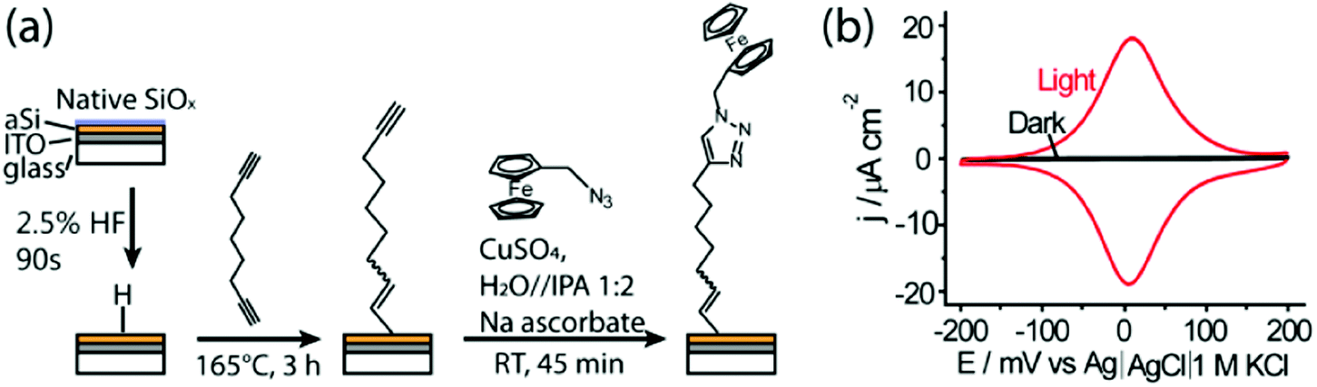 | ||
| Fig. 2 (a) Surface modification of aSi-ITO to attach the redox moiety ferrocene for testing electrochemistry. (b) The cyclic voltammograms for the as modified aSi-ITO in the dark and under light. The scan rate was 100 mV s−1 and the electrolyte was 1 M perchloric acid. | ||
Cyclic voltammetry (CV) was performed for the modified aSi-ITO surface. Light with a power of 94.2 mW cm−2 was illuminated from the backside of the aSi-ITO electrode to activate its conductivity. With 1 M HClO4 as the electrolyte, both oxidation and reduction peaks of ferrocene with a peak separation of only 4 mV were observed in the CV (Fig. 2b). The full width at half maximum of the anodic peak is 90 mV which is extremely close to 90.6 mV, the ideal value of a one electron transfer process.20 No notable faradic current was detected within the same potential window after removal of the illumination due to the drop in the number of charge carriers. Therefore, the 20 nm aSi film on ITO satisfies the ‘switching’ capability to carry out LAE. This photoswitching performance is repeatable, as shown in a chronoamperometry measurement which contained ferrocyanide in the electrolyte to aid the conversion of the oxidized ferricinium back to ferrocene (Fig. S2, ESI†). A similar current was reached as soon as the light was turned on to illuminate the surface and the current dropped rapidly to near zero between the illuminated periods. It is also worth noting that the transparency of the aSi-ITO film was not affected by the electrochemical process (Fig. S3, ESI†). In addition, there is no significant difference in the CV profile for the sample being illuminated from the backside (dry side) or the topside (electrolyte side) (Fig. S4, ESI†). This is in contrast to reports that showed the direction of illumination affected the photoelectrochemical response of the wide band gap semiconductor films on transparent conducting glass. This was because most of the UV light used to excite the charge carrier generation in the wide band gap semiconductor was absorbed by the glass substrate.21 This is one of the benefits of using narrow band gap aSi on ITO as a transparent semiconductor, which allows the electrochemistry to be activated by visible light. In addition, back side illumination is important when performing LAE and high resolution optical microscopy studies simultaneously, as LAE can be integrated by the light source from the transmission mode microscope.
To explore whether aSi-ITO is compatible with high resolution transmission mode microscopy for imaging purpose, HeLa cells were immobilized on an aSi-ITO coverslip, and they were stained with tetramethylrhodamine B isothiocyanate (TRITC) conjugated phalloidin and Hoechst 33342, and imaged using a transmission mode confocal microscope. Cells on a normal glass coverslip (0.17 mm) were also imaged, for the purpose of comparing whether the addition of aSi and ITO bilayers has any effect on the image quality. From Fig. 3a, the cytoskeleton formed by actin filaments (red) is shown clearly along the surface and the body of the cell on aSi-ITO. Individual filopodia projecting from the cell membrane could easily be distinguished (Fig. 3a enlarged). The diameters of the smallest fibrous actin that can be resolved from the image were measured using ImageJ (the number of measurements N = 100). The average diameter of the smallest distinguishable actin on aSi-ITO is 240 ± 52 nm, which is not statistically different from the average diameter of the smallest distinguishable actin from a cell on the normal glass coverslip (220 ± 51 nm). The feature size of 220 nm matches with the expected resolution of the confocal microscope at an emission wavelength of 617 nm for the actin stain used in this experiment. Therefore, the quality of the image for objects on the aSi-ITO coverslip is the same as the objects on the normal glass coverslip. Under the same setting of the confocal microscope, objects on the aSi-ITO may have slightly lower fluorescence intensity, but this can be compensated by adjusting the laser power of the confocal microscope when imaging. Hoechst 33342 stain has the excitation wavelength of 361 nm which is the lowest amongst all the commonly used fluorescent dyes. However, the Hoechst stained nuclei of the cells on the aSi-ITO can still be seen, though the transmittance of the aSi-ITO at that excitation wavelength is less than 10% as known from Fig. 1b. Therefore, the aSi-ITO surfaces are compatible with high resolution transmission mode microscopes.
 | ||
| Fig. 3 (a and b) Fluorescence images of HeLa cells immobilized on the aSi-ITO and 0.17 mm glass coverslip, respectively. The cells have been stained with tetramethylrhodamine B isothiocyanate (TRITC) conjugated phalloidin binding to F-actin and Hoechst 33342 acting on nuclei. F-actin is shown in red and the nucleus is shown in blue in the images. Scale bars are 10 μm. | ||
The capability of the aSi-ITO surface to be used for simultaneous LAE and microscopy imaging was demonstrated by the lysis of MCF-7 cells on the aSi-ITO surface by an electric potential while being monitored using a fluorescence microscope (Fig. 4a). Before the experiment the cells were incubated with the LIVE/DEAD (Calcein-AM/ethidium homodimer-1) stains. As can been seen from Fig. 4b and c, after −0.7 V at 100 Hz frequency was applied to aSi-ITO for 750 s, the cells which were located in the illuminated area of the surface were ruptured, which is shown by the fluorescent signal of the DEAD stain detected under the Cy3 filter, and the morphological changes in the cells including cell membrane swelling and extrusion revealed by the bright field image (Fig. S5, ESI†). In contrast, no cell rupturing or other changes were detected for the cells that were not in the illuminated area of the surface (Fig. 4d and e), indicating that they have not been influenced by the application of electric potential.
 | ||
| Fig. 4 (a) Illustration of localized cell lysis using light activated electrochemistry which was reflected by fluorescence microscopy. The merged fluorescent images of the LIVE/DEAD stained MCF-7 cells (b and d) before and (c and e) after the ferrocene attached aSi-ITO surface was subjected to −0.7 V at 100 Hz frequency for 750 s. (b and c) are cells from the area which was exposed to light from the microscope objective, and (d and e) are cells from the area which has not been exposed to the light from the microscope during the application of the electric potential. Green colour indicates live cells and red colour indicates damaged cells. Scale bars are 50 μm. | ||
In summary, we report here that LAE can be performed on a 20 nm aSi film on an ITO surface. Having such a thin aSi layer on the transparent conducting glass does not affect the quality of the fluorescent images obtained for the object on this surface. With these two features, this platform is able to perform simultaneous LAE and fluorescence imaging. This opens up opportunities to study localised heterogeneous events on a macroelectrode by combining both imaging and localized electrochemical measurements. The application of this platform for rare single cell sensing and manipulation is under investigation. As the substrate itself is transparent and a narrow band gap semiconductor, it can also be a material of interest for other applications including photovoltaics.
This research was supported by the ARC Centre of Excellence in Convergent Bio-Nano Science and Technology (CE140100036) and ARC Laureate Fellowship (FL150100060) program. We would also like to acknowledge the Australian National Fabrication Facility (ANFF) ACT node, the Mark Wainwright Analytical Centre for access to the facilities used in this work.
Conflicts of interest
There are no conflicts to declare.Notes and references
- Z. Lin, Y. Takahashi, Y. Kitagawa, T. Umemura, H. Shiku and T. Matsue, Anal. Chem., 2008, 80, 6830–6833 CrossRef CAS.
- A. J. Bard, F. R. F. Fan, J. Kwak and O. Lev, Anal. Chem., 1989, 61, 132–138 CrossRef CAS.
- M. H. Choudhury, S. Ciampi, Y. Yang, R. Tavallaie, Y. Zhu, L. Zarei, V. R. Goncales and J. J. Gooding, Chem. Sci., 2015, 6, 6769–6776 RSC.
- L. Zarei, R. Tavallaie, M. H. Choudhury, S. G. Parker, P. Bakthavathsalam, S. Ciampi, V. R. Gonçales and J. J. Gooding, Langmuir, 2018 DOI:10.1021/acs.langmuir.8b02222.
- Y. B. Vogel, V. R. Gonçales, J. J. Gooding and S. Ciampi, J. Electrochem. Soc., 2018, 165, H3085–H3092 CrossRef CAS.
- S. G. Parker, Y. Yang, S. Ciampi, B. Gupta, K. Kimpton, F. M. Mansfeld, M. Kavallaris, K. Gaus and J. J. Gooding, Nat. Commun., 2018, 9, 2288 CrossRef PubMed.
- H. Wu, D. Kong, Z. Ruan, P.-C. Hsu, S. Wang, Z. Yu, T. J. Carney, L. Hu, S. Fan and Y. Cui, Nat. Nanotechnol., 2013, 8, 421 CrossRef CAS PubMed.
- M. Parviz, K. Gaus and J. J. Gooding, Chem. Sci., 2017, 8, 1831–1840 RSC.
- R. Peat, A. R. Kucernak and D. E. Williams, Electrochim. Acta, 1992, 37, 933–942 CrossRef CAS.
- A. Meunier, O. Jouannot, R. Fulcrand, I. Fanget, M. Bretou, E. Karatekin, S. Arbault, M. Guille, F. Darchen, F. Lemaître and C. Amatore, Angew. Chem., 2011, 123, 5187–5190 CrossRef.
- J. M. Salverda, A. V. Patil, G. Mizzon, S. Kuznetsova, G. Zauner, N. Akkilic, G. W. Canters, J. J. Davis, H. A. Heering and T. J. Aartsma, Angew. Chem., Int. Ed., 2010, 49, 5776–5779 CrossRef CAS.
- X. Lu, P. R. Nicovich, M. Zhao, D. J. Nieves, M. Mollazade, S. R. C. Vivekchand, K. Gaus and J. J. Gooding, Nat. Commun., 2018, 9, 3320 CrossRef.
- M. I. Kabir, S. A. Shahahmadi, V. Lim, S. Zaidi, K. Sopian and N. Amin, Int. J. Photoenergy, 2012, 7 Search PubMed.
- Y. Abdulraheem, I. Gordon, T. Bearda, H. Meddeb and J. Poortmans, AIP Adv., 2014, 4, 057122 CrossRef.
- X. Meng, V. Depauw, G. Gomard, O. El Daif, C. Trompoukis, E. Drouard, C. Jamois, A. Fave, F. Dross, I. Gordon and C. Seassal, Opt. Express, 2012, 20, A465–A475 CrossRef CAS.
- Y. Yang, S. Ciampi and J. J. Gooding, Langmuir, 2017, 33, 2497–2503 CrossRef CAS.
- S. Ciampi, P. K. Eggers, G. Le Saux, M. James, J. B. Harper and J. J. Gooding, Langmuir, 2009, 25, 2530–2539 CrossRef CAS.
- S. Ciampi, M. James, G. Le Saux, K. Gaus and J. Justin Gooding, J. Am. Chem. Soc., 2012, 134, 844–847 CrossRef CAS.
- S. Ciampi, M. James, P. Michaels and J. J. Gooding, Langmuir, 2011, 27, 6940–6949 CrossRef CAS.
- E. Laviron, J. Electroanal. Chem. Interfacial Electrochem., 1972, 39, 1–23 CrossRef CAS.
- I. Bedja, S. Hotchandani and P. V. Kamat, J. Phys. Chem., 1994, 98, 4133–4140 CrossRef CAS.
Footnote |
| † Electronic supplementary information (ESI) available: XPS characterization of the modified surface, additional UV-Vis and electrochemical data and experimental methods. See DOI: 10.1039/c8cc07889k |
| This journal is © The Royal Society of Chemistry 2019 |