
 Open Access Article
 This Open Access Article is licensed under a
 Creative Commons Attribution 3.0 Unported Licence
Determination of the graphene–graphite ratio of graphene powder by Raman 2D band symmetry analysis†
Sarah
Roscher
 *,
René
Hoffmann
and
Oliver
Ambacher
*,
René
Hoffmann
and
Oliver
Ambacher
Fraunhofer Institute for Applied Solid State Physics IAF, Tullastraße 72, D-79108 Freiburg, Germany. E-mail: Sarah.roscher@iaf.fraunhofer.de
First published on 24th January 2019
Abstract
Graphene has many unique properties which make it an attractive material for many applications. Analytical methods to differentiate graphene from graphite, like the optical contrast technique, atomic force microscopy or conventional Raman analysis based on intensity ratios, require a specific sample preparation and substrate. Here we report a method to distinguish between few-layer graphene (with less than 10 layers) and graphite that is independent of a specific sample preparation or substrate. Our approach is based on the symmetry of the Raman 2D peak in graphene and its asymmetry in graphite. By evaluating the coefficient of determination R2 of a Voigt profile fit we can establish a benchmark that discerns graphene from graphite. We found values above 0.985 to be characteristic of graphene. The results were confirmed by thickness measurements with atomic force microscopy. We applied this analysis to both individual graphene flakes and graphene flakes as a thick film. This method allows for fast characterisation of large quantities, a feature that is needed for industrial application. It can be used to determine the graphene content of flakes produced from graphite exfoliation and the efficiency of various production methods.
Introduction
Graphene, a monolayer of carbon atoms arranged in a honeycomb lattice, has attracted great interest from both researchers and industry worldwide due to its many outstanding properties like high electrical conductivity,1 transparency,2 and mechanical strength3 to name a few. For applications not only is single layer graphene (SLG) of interest, but also few-layer graphene (FLG),4–8 in particular for the use of graphene flakes. The boundary between graphene and graphite properties is a layer number of 10.9,10 This is due to the fact that the electronic structure evolves with the number of layers and at 10 layers it approaches that of graphite.4,11 Therefore, a method for distinguishing between FLG and graphite is needed. Furthermore, with many graphene flake producers emerging in the market the need for quality determination and control arises. With graphene flakes, which are produced by exfoliation from graphite, there will always be a distribution of flake thickness present in the resulting material12 and oftentimes also flakes with more than ten layers, and thus graphite. This exfoliation degree needs to be determined to judge the efficiency of methods and to assess the quality for applications.Until now the layer number has been determined by the optical contrast technique.1 However this technique can only be used in relative thickness comparison and depends on the optical elements used in the measurements.13–15 Other methods are atomic force microscopy (AFM) or transmission electron microscopy, but both are very time consuming and laborious especially for characterizing large quantities. The most commonly used approach is based on Raman spectroscopy, which offers a fast and practical tool for graphene analysis. The characteristics of graphene in Raman spectroscopy are well studied.16,17 Typically the layer number is determined by the intensity ratio of the G and 2D bands18 or its full width at half maximum (FWHM).18,19 However, they are impaired by stress, unintentional doping and annealing.20–23 Another approach is based on the intensity of the graphene G band relative to the Raman band of an underlying silicon substrate.24 The disadvantage of this and all the aforementioned methods is the requirement of carefully separated graphene flakes and the use of a specific substrate.
Here we present a straightforward, robust approach to differentiate graphene from graphite using Raman spectroscopy and a fit of the 2D band that is also applicable to non-isolated graphene flakes, e.g., as a film or powder, and is independent of the preparation method or substrate.
Experimental
Materials and sample preparation
As a reference for the SLG Raman spectrum, graphene was grown by chemical vapour deposition on copper foil as described elsewhere.25 For the graphite Raman spectrum reference natural graphite flakes were obtained from Schunk Hoffmann Carbon Technologies AG, Austria. The graphene flakes, containing both FLG and graphite, were produced from the graphite flakes by electrochemical expansion and subsequent thermal exfoliation as described elsewhere.26 For AFM and Raman mapping analysis the flakes were prepared on a silicon substrate with a 300 nm oxide layer by dip-coating. For the Raman analysis of graphene flakes as a thick film, the flakes were pasted on glass. The graphite was measured as pellets and the CVD graphene grown on copper.Raman measurement
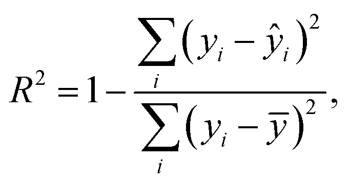
Spectra were obtained with an InVia Raman microscope with a 532 nm excitation laser, 1800 mm−1 grating and a spatial resolution of 1 μm from Renishaw, Gloucestershire, UK.For the analysis of the spectra a baseline subtraction was carried out followed by fitting of the 2D band with a single Voigt profile. For this fit the coefficient of determination R2 was calculated as usual by using
AFM measurements
AFM measurements were performed under ambient conditions using a NanoWizard 3 System (NanoWizard 3, JPK Instruments) in tapping mode with a PPP-NCHR AFM probe.Results and discussion
Graphene and graphite show four peaks in the Raman spectrum as depicted in Fig. 1. The D band around 1350 cm−1 originates from transverse optical phonons around the Brillouin zone corner K. It is due to the breathing modes of the six-atom rings of graphene and requires a defect for its activation. For both graphite and graphene, the D peak is small indicating a low defect density of the used materials. The faint peak at around 2450 cm−1 is assigned to a combination of a D phonon and an acoustic longitudinal phonon (D′′) and thus called D + D′′. The G band around 1590 cm−1 is due to first-order Raman scattering by doubly degenerate in-plane vibration modes (in-plane optical transverse and longitudinal phonons) at the Brillouin zone centre. The 2D band at around 2680 cm−1 is due to second-order Raman scattering by in-plane transverse optical phonons near the boundary of the Brillouin zone and is closely linked to the electronic band structure.16 In the case of SLG the 2D band is symmetric. With increasing layer number a splitting of the electronic band structure at the K point occurs leading to a broadening of the 2D band.16,19 The band structure approaches that of graphite at 10 layers4,11 at which point the Raman 2D band becomes indistinguishable from that of graphite. The 2D band of graphite consists of 2 components and is strongly asymmetric (see Fig. 1). This difference of the Raman 2D band shape can be used to confidently distinguish between graphene and graphite. While SLG can be fitted with one Lorentzian peak and graphite with two based on their band structure, the case of FLG is complicated, since the electronic structure and the underlying phonon scattering processes are more complex.27 The 2D band shape is also affected by doping and stress22,28 causing a broadening and influencing the peak shape, making an exact fit with multiple components difficult. Therefore, as a more straightforward approach we are using the basic difference between the asymmetric 2D band shape of graphite and the symmetric band shape of graphene. By fitting the 2D band with a single, symmetric Voigt profile this symmetry can be evaluated. Since the 2D band of FLG is still mostly symmetric18,19,29 this approach also includes FLG. Therefore, it allows us to determine the content of FLG versus graphite and thus the exfoliation efficiency of production methods.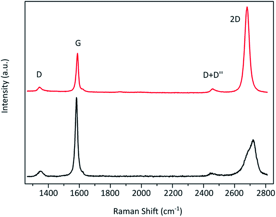 | ||
| Fig. 1 Raman spectrum of CVD grown SLG (red) and graphite (black). | ||
In Fig. 2 the Raman 2D band of CVD grown SLG and that of graphite are shown, fitted with one Voigt peak. To judge the symmetry, we looked at the fit's coefficient of determination R2. It is an indication of how well the fit approximates the data. In the case of the highly symmetric peak of SLG the R2 value is nearly 1 (Fig. 2a). The more asymmetric, the more the fit deviates from the data leading to a low R2 value for graphite. Looking at the statistical distribution of R2 values of over 100 spectra of each sample (Fig. 3), there is a clear difference between graphene and graphite. SLG shows consistently R2 values above 0.985 with most of them being between 0.998 and 1.0. The slight deviations are due to noise of the data and non-intentional doping and stress of the graphene sample. The graphite sample on the other hand generally exhibits R2 values below 0.985, where spectra with clearly two components in the 2D band have a very low value (see Fig. 2b). In the case of a nearly symmetrical shape the value comes close to 0.985 (see Fig. 2c). Therefore, this value of 0.985 marks the transition of symmetric to asymmetric 2D peak shapes and thus can be used as a benchmark to differentiate between graphite and graphene, and by extension, FLG.
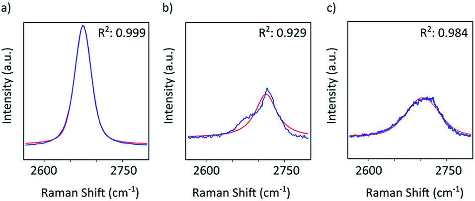 | ||
| Fig. 2 Raman 2D band of (a) SLG and (b) and (c) graphite. All plots show the measured data in blue and the Voigt profile fit in red together with the resulting coefficient of determination R2. | ||
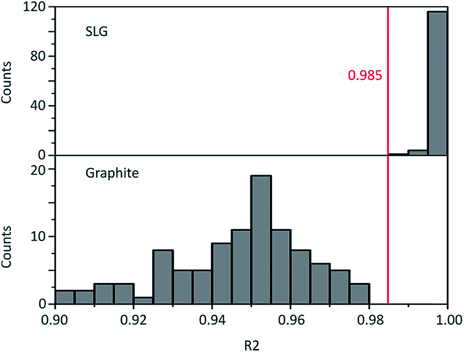 | ||
| Fig. 3 Histogram of the Raman 2D band fit coefficient R2 of SLG and graphite. Their distributions are significantly different with a p-value below 0.05 as determined by a two-sample t-test. | ||
To verify the effectiveness of this approach and its applicability to the evaluation of the graphene content of flakes from graphite exfoliation the Raman fitting was correlated to AFM thickness determination. Flakes produced by exfoliation of graphite were investigated. As with all exfoliation methods the resulting material contains flakes of varying thickness and thus both graphite and graphene flakes. These flakes were prepared on a silicon substrate with a 300 nm oxide layer. Then spatially resolved μ-Raman measurement and 2D band fitting were carried out along with AFM measurement. The resulting Raman image obtained from the 2D band fit's coefficient of determination R2 is shown in Fig. 4b with the corresponding AFM images Fig. 4c. R2 values below the graphite benchmark of 0.985 are depicted in blue, values above in red, and areas with no flakes in black. The map matches well with the optical microscopy and AFM measurement. The long thick graphite flake has a height of more than 40 nm and is thus more than 10 layers thick. It displays R2 values below 0.985 as expected. The same is the case for the other flake at the bottom of the image, which with more than 12 nm is also graphite. The area surrounding the graphite flake exhibits R2 values above 0.985 indicating graphene flakes with less than 10 layers. Their detailed AFM image and profiles can be seen in the ESI.† Their heights were determined to be 3 nm or less. Considering a hydration layer between the graphene flake and substrate of 0.5–1.5 nm![[thin space (1/6-em)]](https://www.rsc.org/images/entities/char_2009.gif) 1,30 and a graphene layer thickness of around 0.4 nm1,30 these flakes consist of about 5 layers or fewer. Thus the AFM height measurements are in accordance with the Raman R2 distinction method. However, there are areas on both graphite flakes (marked with green circles in Fig. 4) where the R2 value is above 0.985 and thus indicating graphene, which seems to be in contradiction with the AFM measured heights. But in the AFM error signal image (Fig. 4d), which offers better visual contrast, it can be seen that in these areas thinner flakes are lying on top of the graphite flakes (circled in green). While Raman spectroscopy is a surface sensitive method, penetration and detection depths are still around 50 nm and thus more than the thickness of those FLG flakes. However, it was found that FLG gives a higher Raman intensity than graphite.31 Therefore, these overlying graphene flakes likely dominate the Raman 2D signal. The histogram of the R2 values for this area is shown in the ESI.† The R2 value distribution of the investigated FLG flakes was found to be significantly different from the determined threshold value of 0.985 with a p-value below 0.05 as determined by a one-tailed, one-sample t-test. From the R2 analysis in correlation with AFM measurements we can conclude that the established threshold of 0.985 can be used to distinguish FLG from graphite.
1,30 and a graphene layer thickness of around 0.4 nm1,30 these flakes consist of about 5 layers or fewer. Thus the AFM height measurements are in accordance with the Raman R2 distinction method. However, there are areas on both graphite flakes (marked with green circles in Fig. 4) where the R2 value is above 0.985 and thus indicating graphene, which seems to be in contradiction with the AFM measured heights. But in the AFM error signal image (Fig. 4d), which offers better visual contrast, it can be seen that in these areas thinner flakes are lying on top of the graphite flakes (circled in green). While Raman spectroscopy is a surface sensitive method, penetration and detection depths are still around 50 nm and thus more than the thickness of those FLG flakes. However, it was found that FLG gives a higher Raman intensity than graphite.31 Therefore, these overlying graphene flakes likely dominate the Raman 2D signal. The histogram of the R2 values for this area is shown in the ESI.† The R2 value distribution of the investigated FLG flakes was found to be significantly different from the determined threshold value of 0.985 with a p-value below 0.05 as determined by a one-tailed, one-sample t-test. From the R2 analysis in correlation with AFM measurements we can conclude that the established threshold of 0.985 can be used to distinguish FLG from graphite.
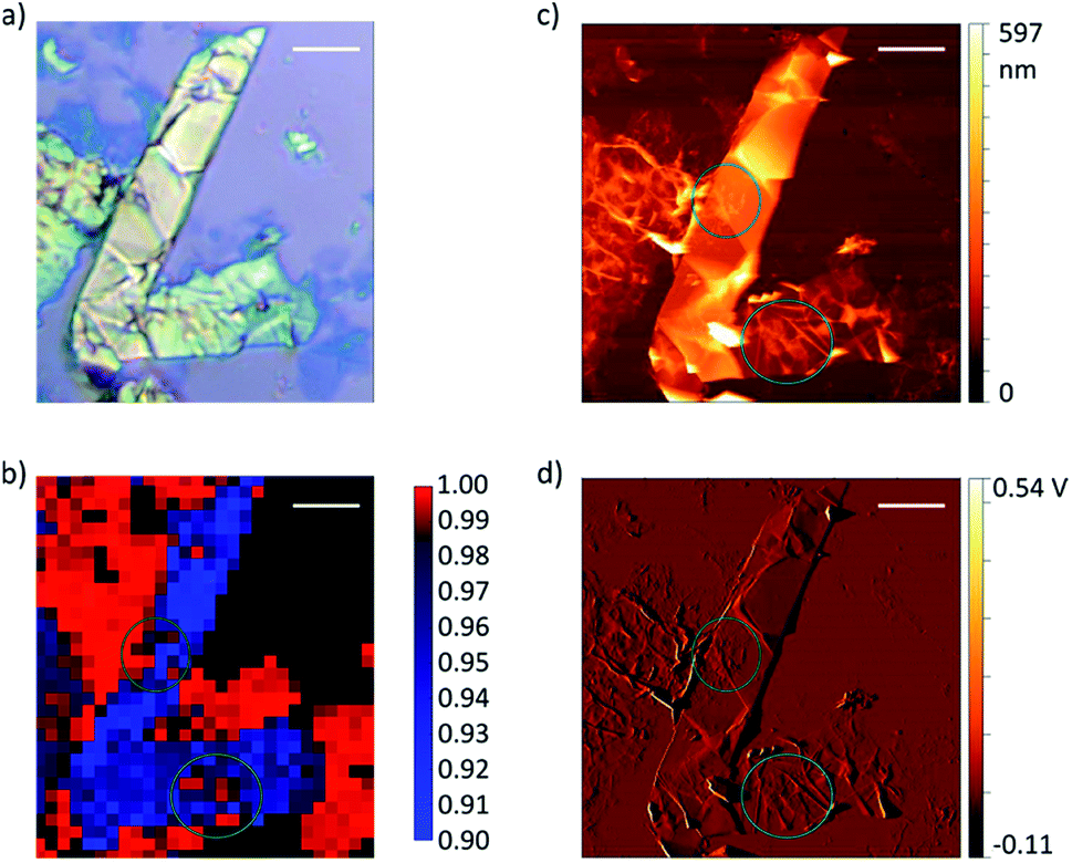 | ||
| Fig. 4 Graphite and graphene flakes on SiO2 (300 nm)/Si. (a) shows the optical microscope image of that area, and (b) shows the coefficient of determination R2 of the Raman 2D band fit with values considered as graphite in blue, as graphene in red and the substrate in black. (c) and (d) depict the AFM measured height and error signal respectively. Scale bars are 5 μm. | ||
Since for this analysis there is no need for a specific underlying substrate nor the careful separation of graphene flakes, its great advantage is the applicability to thick films or powder samples, in which graphene flakes are usually readily available and handled. This not only supersedes additional preparation steps but also allows flexible integration in processing lines. In Fig. 5 the R2 histogram of the same material containing both FLG and graphite flakes measured in powder form is shown. It exhibits a broader distribution of R2 values both below and above 0.985 with separate distributions visible resulting from the presence of both graphene and graphite flakes. Using the R2 distinction we can determine the graphite content and exfoliation efficiency of the production method.
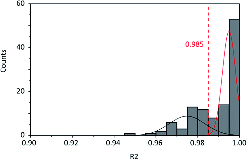 | ||
| Fig. 5 Histogram of R2 from the 2D band fit of partially exfoliated flakes, containing both graphite and graphene flakes. The black and red lines represent the distribution of graphite and graphene flakes to guide the eye. Their distributions are significantly different with a p-value below 0.05 as determined by a two-sample t-test. | ||
Conclusions
We demonstrated a straightforward approach to confidently distinguish between graphene (less than 10 layers) and graphite based on Raman spectroscopy and analysis of the 2D band for symmetry using a Voigt peak fit. The resulting value of the coefficient of determination R2 offers a gauge with a limit of more than 0.985 indicating graphene. We evaluated our method using AFM measurements and found good agreement. The advantage of this method is its independency from the substrate and the possibility to measure powdered bulk graphene flakes while also being more robust concerning nonintentional stress and doping.Conflicts of interest
There are no conflicts to declare.Acknowledgements
We gratefully acknowledge funding by the Sustainability Centre Freiburg (project G-ONET).References
- K. S. Novoselov, A. K. Geim, S. V. Morozov, D. Jiang, Y. Zhang, S. V. Dubonos, I. V. Grigorieva and A. A. Firsov, Science, 2004, 306, 666–669 CrossRef CAS.
- K. F. Mak, L. Ju, F. Wang and T. F. Heinz, Solid State Commun., 2012, 152, 1341–1349 CrossRef CAS.
- C. Lee, X. Wei, J. W. Kysar and J. Hone, Science, 2008, 321, 385–388 CrossRef CAS PubMed.
- A. K. Geim and K. S. Novoselov, Nat. Mater., 2007, 6, 183–191 CrossRef CAS PubMed.
- B. Mendoza-Sánchez, B. Rasche, V. Nicolosi and P. S. Grant, Carbon, 2013, 52, 337–346 CrossRef.
- F. Torrisi, T. Hasan, W. Wu, Z. Sun, A. Lombardo, T. S. Kulmala, G.-W. Hsieh, S. Jung, F. Bonaccorso, P. J. Paul, D. Chu and A. C. Ferrari, ACS Nano, 2012, 6, 2992–3006 CrossRef CAS PubMed.
- J. Li, M. M. Naiini, S. Vaziri, M. C. Lemme and M. Östling, Adv. Funct. Mater., 2014, 24, 6524–6531 CrossRef CAS.
- X. Li, Y. Zhu, W. Cai, M. Borysiak, B. Han, D. Chen, R. D. Piner, L. Colombo and R. S. Ruoff, Nano Lett., 2009, 9, 4359–4363 CrossRef CAS PubMed.
- International Organization for Standardization, Nanotechnologies – Vocabulary – Part 13: Graphene and related two-dimensional (2D) materials, 2017, ISO/TS 80004-13:2017 Search PubMed.
- A. Bianco, H.-M. Cheng, T. Enoki, Y. Gogotsi, R. H. Hurt, N. Koratkar, T. Kyotani, M. Monthioux, C. R. Park, J. M. Tascon and J. Zhang, Carbon, 2013, 65, 1–6 CrossRef CAS.
- B. Partoens and F. M. Peeters, Phys. Rev. B: Condens. Matter Mater. Phys., 2006, 74 Search PubMed.
- V. Palermo, I. A. Kinloch, S. Ligi and N. M. Pugno, Adv. Mater., 2016, 28, 6232–6238 CrossRef CAS PubMed.
- Z. H. Ni, H. M. Wang, J. Kasim, H. M. Fan, T. Yu, Y. H. Wu, Y. P. Feng and Z. X. Shen, Nano Lett., 2007, 7, 2758–2763 CrossRef CAS.
- L. Gao, W. Ren, F. Li and H.-M. Cheng, ACS Nano, 2008, 2, 1625–1633 CrossRef CAS.
- K. Nagashio, T. Nishimura, K. Kita and A. Toriumi, Appl. Phys. Express, 2009, 2, 025003 CrossRef.
- A. C. Ferrari, J. C. Meyer, V. Scardaci, C. Casiraghi, M. Lazzeri, F. Mauri, S. Piscanec, D. Jiang, K. S. Novoselov, S. Roth and A. K. Geim, Phys. Rev. Lett., 2006, 97, 187401 CrossRef CAS PubMed.
- A. C. Ferrari, Solid State Commun., 2007, 143, 47–57 CrossRef CAS.
- D. Graf, F. Molitor, K. Ensslin, C. Stampfer, A. Jungen, C. Hierold and L. Wirtz, Nano Lett., 2007, 7, 238–242 CrossRef CAS PubMed.
- Y. Hao, Y. Wang, L. Wang, Z. Ni, Z. Wang, R. Wang, C. K. Koo, Z. Shen and J. T. L. Thong, Small, 2010, 6, 195–200 CrossRef CAS PubMed.
- B. Tang, H. Guoxin and H. Gao, Appl. Spectrosc. Rev., 2010, 45, 369–407 CrossRef CAS.
- W. Xueshen, L. Jinjin, Z. Qing, Z. Yuan and Z. Mengke, J. Nanomater., 2013, 2013, 1–6 CrossRef.
- A. Das, S. Pisana, B. Chakraborty, S. Piscanec, S. K. Saha, U. V. Waghmare, K. S. Novoselov, H. R. Krishnamurthy, A. K. Geim, A. C. Ferrari and A. K. Sood, Nat. Nanotechnol., 2008, 3, 210–215 CrossRef CAS PubMed.
- T. M. G. Mohiuddin, A. Lombardo, R. R. Nair, A. Bonetti, G. Savini, R. Jalil, N. Bonini, D. M. Basko, C. Galiotis, N. Marzari, K. S. Novoselov, A. K. Geim and A. C. Ferrari, Phys. Rev. B: Condens. Matter Mater. Phys., 2009, 79, 424 CrossRef.
- Y. K. Koh, M.-H. Bae, D. G. Cahill and E. Pop, ACS Nano, 2011, 5, 269–274 CrossRef CAS.
- M. Knapp, R. Hoffmann, V. Cimalla and O. Ambacher, Nanomaterials, Basel, Switzerland, 2017, vol. 7 Search PubMed.
- R. Hoffmann, S. Roscher and C. E. Nebel, PCT/EP2016/073451, 2016.
- J. S. Park, A. Reina, R. Saito, J. Kong, G. Dresselhaus and M. S. Dresselhaus, Carbon, 2009, 47, 1303–1310 CrossRef CAS.
- Z. H. Ni, H. M. Wang, Z. Q. Luo, Y. Y. Wang, T. Yu, Y. H. Wu and Z. X. Shen, J. Raman Spectrosc., 2010, 41, 479–483 CrossRef CAS.
- Z. H. Ni, H. M. Wang, Y. Ma, J. Kasim, Y. H. Wu and Z. X. Shen, ACS Nano, 2008, 2, 1033–1039 CrossRef CAS PubMed.
- M. Temmen, O. Ochedowski, M. Schleberger, M. Reichling and T. R. J. Bollmann, New J. Phys., 2014, 16, 53039 CrossRef.
- Z. Ni, Y. Wang, T. Yu and Z. Shen, Nano Res., 2008, 1, 273–291 CrossRef CAS.
Footnote |
| † Electronic supplementary information (ESI) available. See DOI: 10.1039/c8ay02619j |
| This journal is © The Royal Society of Chemistry 2019 |