
 Open Access Article
 This Open Access Article is licensed under a
 Creative Commons Attribution 3.0 Unported Licence
Characterisation of thin boron-doped diamond films using Raman spectroscopy and chemometrics†
Peter
Knittel
 *a,
Robert
Stach
b,
Taro
Yoshikawa
a,
Lutz
Kirste
a,
Boris
Mizaikoff
b,
Christine
Kranz
b and
Christoph E.
Nebel
a
*a,
Robert
Stach
b,
Taro
Yoshikawa
a,
Lutz
Kirste
a,
Boris
Mizaikoff
b,
Christine
Kranz
b and
Christoph E.
Nebel
a
aFraunhofer IAF, Institute for Applied Solid State Physics, Tullastraße 72, 79108 Freiburg, Germany. E-mail: peter.knittel@iaf.fraunhofer.de
bUlm University, Institute of Analytical and Bioanalytical Chemistry, Albert-Einstein-Allee 11, 89081 Ulm, Germany
First published on 26th December 2018
Abstract
Diamond coatings are characterised by outstanding mechanical and chemical robustness and hence, thin diamond layers doped with boron are particularly interesting for transparent electrodes, e.g., for spectroelectrochemical applications. In this study, we present a non-destructive chemometric method to determine thickness and boron concentration of as-deposited heavily doped diamond films on silicon substrates, which may be used, e.g., as electroactive infrared transparent windows. Using partial least-squares regression, we readily predicted these parameters with high accuracy from Raman spectra after calibration with a set of diamond films, previously characterised by secondary ion mass spectrometry. Due to the Fano resonance caused by the boron incorporation into the diamond lattice, which is observable in the Raman spectrum, a precise determination of the boron concentration is possible. In addition, for diamond films below the wavelength of the used Raman laser, we were able to determine the thickness of the as-grown films and gain information on the underlying substrate.
Introduction
Apart from its excellent robustness and the chemical inertness, a wide optical window from the near-ultraviolet (UV) to the far-infrared (IR) makes diamond particularly attractive as a transparent functional material.1 Nowadays, diamond is routinely synthesised using, e.g., microwave plasma enhanced chemical vapour deposition (MWCVD).2 By incorporation of boron, electrical conductivity can be achieved and tuned.3 Apart from the robustness, these boron-doped diamond (BDD) electrodes show excellent electrochemical properties namely a wide electrochemical window in aqueous solution, low background currents, and are less prone to fouling even under physiological conditions.4 Thus, they are commonly used for electroanalytical applications like heavy metal detection,5 pH sensing,6 electrochemical conversions,7 and other emerging areas.8 For such applications, the boron concentration plays an important role as it influences the electroanalytical performance.9,10 In addition, boron incorporation into the diamond lattice largely influences the transmission properties as observable from the dark colour of doped diamond films.Especially in the IR range, the conductivity plays a major role for the transmission properties. Heavily doped layers (>1021 atoms per cm3) have nearly metallic conductivity (100 S cm), and hence they are strong IR absorbers arising from the complex refractive index.11 Nevertheless, when using nanometer-sized films, the influence on transmission properties can be minimized drastically which paves the way for the manufacturing of transparent contacts and electrodes, e.g., for spectroelectrochemical applications.12 Up to now only a few studies on optically transparent electrodes (OTE) have been conducted, e.g., for spectroelectrochemical measurements on the ferrocene redox couple,13 or a multi-analytical platform for atomic force microscopy combined with IR measurements and electrochemistry.14 A reason for that may be the rather challenging fabrication of such OTEs, which afford well-controlled growth conditions and high reproducibility concerning uniformity, thickness, and dopant concentration.
We recently succeeded in growing ultrathin, pinhole-free diamond layers with thicknesses down to 50 nm.15 Such films are highly attractive for conductive coatings on optically transparent substrates. However, as they are grown within the early stages of the diamond synthesis, controlling both, the dopant concentration as well as the thickness is challenging. To ensure successful growth and reliable quality, a fast and non-destructive characterisation method is mandatory.
Commonly these parameters are obtained using secondary-ion mass spectrometry (SIMS), which even provides a depth profile of dopants in the grown diamond layer, but is destructive.16 The boron concentration may also be determined using cathodoluminescence, which affords a sophisticated, expensive setup,17 or Mott–Schottky analysis, where interpretation is challenging and parasitic capacitance may readily spoil the measurement.18 Apart from that, other methods have been established including Raman spectroscopy that has been used, e.g., to study the influence of boron incorporation on the diamond Raman line at 1332 cm−1. The dopant concentration can be estimated using the Fano-resonance caused by the boron incorporation.19,20
In a similar approach and in order to provide a fast, non-destructive and non-invasive method for the detection of both, the boron concentration and the thickness of thin boron doped diamond layers grown on IR transparent samples like silicon, we have developed a chemometric method based on partial least squares regression (PLSR) using Raman spectra of the as-grown diamond layers.21,22 For this purpose, a set of diamond films was grown and characterised by SIMS measurements. This set was used to develop and validate a chemometric model. Applying a PLSR model to a dataset in the present size, potentially decreases the number of variables by taking into account the most relevant variances for a number of features within the spectral data. Thus, the model is capable of both, predicting thickness and the dopant concentration simultaneously within a few seconds and high accuracy using the recorded Raman spectral data.
To further optimize the spectral calibration set in terms of size and avoiding collinearities, it was calculated via an experimental design.23 Additionally, the model was found to be sensitive to characteristics of the substrate, e.g., the conductivity of underlying silicon wafer, which helps to characterise the coated element as a whole.
Experimental
Sample preparation
As substrates prime grade 4′′ silicon wafers were used: low-doped with a resistivity in the range of 10–50 Ω cm and heavily doped with a resistivity of 0.01–0.02 Ω cm, both p-type, using boron as dopant (Si-Mat, Germany). Nanodiamond seeding was carried out using 4 nm hydrogen-terminated nanodiamonds (G01 grade, Plasmachem GmbH, Germany) following a procedure described elsewhere.24,25 Briefly, as-received nanodiamonds are hydrogen-terminated by annealing in H2 atmosphere and then dispersed in 10−3 M KCl aqueous solution. A pulsed ultrasonic treatment is used to break up agglomerates and the resulting solution is further centrifuged for 8 h at 40 kg RCF to separate agglomerates and obtain a seeding solution mainly consisting of individual nanodiamond particles (as confirmed via dynamic light scattering). All substrates were RCA cleaned before use, then immersed into the seeding solution and treated in an ultrasonic bath for 5 min. After rinsing with ultrapure water, the wafers were spin-dried and loaded into the reactor.MWCVD growth
Diamond growth was carried out in an ellipsoidal MPCVD reactor using purified gases (hydrogen, methane, and trimethylborane (TMB)).2 The used reactor design can load samples up to 6′′. For all grown samples the growth conditions were identical at 9 kW microwave power, 750 °C substrate temperature, 50 mbar pressure and a methane concentration of 2% in H2. By varying the B/C ratio (300–2000 ppm), i.e., TMB concentration and the deposition time, a set of 15 diamond films were grown (1–11, C1–C4), of which 4 films were grown on IR non-transparent, conductive silicon denoted as C1 to C4, as shown in Table 1.| ID | Thickness/nm | B concentration/1020 cm−3 | Substrate resistivity/Ω | Roughness RMS/nm |
|---|---|---|---|---|
| 1 | 60 | 7.47 | 4 | 12.9 |
| 2 | 100 | 24.7 | 20 | 15.0 |
| 3 | 165 | 33.3 | 10 | 20.1 |
| 4 | 200 | 21.7 | 7 | 30.9 |
| 5 | 220 | 23.2 | 9 | 28.9 |
| 6 | 270 | 21.8 | 13 | 29.4 |
| 7 | 300 | 16.2 | 8 | 36.0 |
| 8 | 450 | 14.2 | 10 | 40.4 |
| 9 | 470 | 17.1 | 7.5 | 41.4 |
| 10 | 520 | 32.3 | 7 | 35.6 |
| 11 | 620 | 30.4 | 4 | 42.5 |
| C1 | 90 | 18.9 | 0.02 | 16.2 |
| C2 | 240 | 24.6 | 0.06 | 31.7 |
| C3 | 245 | 30.7 | 0.09 | 30.8 |
| C4 | 370 | 6.39 | 0.05 | 39.0 |
Characterisation and data processing
The as-grown samples were characterised using SIMS measurements (Atomika 4500, Cameca, France) to obtain thickness and dopant concentration. Also the substrate resistivity was measured using a 4-point probe (MCP-T-700, Mitsubishi Chemical Analytech, Japan). These measurements served as a reference for the chemometric model. Additionally, the films were characterised by atomic force microscopy (NanoWizard III, JPK Instruments, Germany) and transmission IR spectroscopy (Vertex 70, Bruker, Germany) (Fig. S1,†2).For the chemometric model, Raman spectra were recorded with a Raman microscope (InVia, Renishaw, UK) using a laser with a wavelength of 532 nm. All samples were measured at least 3 times (2 s exposure, 5 spectra averaged) at 3 independent spots of the individual diamond-coated samples. The PLSR was then carried out using the PLS-Toolbox (Eigenvector Research, USA) and MATLAB (MathWorks, USA). Data processing was kept at a minimum including a baseline correction (automatic weighted least squares), taking the decadic logarithm, and auto scaling as prerequisite for PLSR. Eight latent variables (LVs) were selected, which contain approx. 88% variance within the calibration data set. The number of LVs is based on the cumulative variance captured by the model in order to achieve a maximum predictability without taking artefacts and noise into account. This validation was carried out via a random data split of 41 samples out of the dataset (calibration set has 162 samples).21 For the calibration set, an experimental design algorithm was applied via the mixexp software package for R statistics, i.e., a x-vertices design.23
Results and discussion
Diamond film growth
For this study, a set of diamond films were grown, which was further characterised in detail by SIMS, AFM, IR and Raman spectroscopy. Growth parameters were optimized for the used substrates in terms of growth temperature, sp2-content and film uniformity. For an IR transparent electrode, the diamond film should show good conductivity and low absorption in the spectral window of interest. Thus, the calibration set was chosen in a range of 5 × 10²⁰ to 3 × 10²¹ atoms per cm3 (2800–17![[thin space (1/6-em)]](https://www.rsc.org/images/entities/char_2009.gif) 000 ppm) for the boron concentration with a targeted film thickness of 50–600 nm. In order to study the influence of the underlying substrate on the chemometric model, diamond films were also grown on 4 conductive silicon wafers (0.01–0.02 Ω cm). Due to the short growth times, the synthesis of thin diamond layers is challenging. Depending on the reactor type and growth parameters, constant conditions are not reached until the end of the process. This is clearly visible in the average growth rate obtained after different growth times (Fig. 1a). For the used reactor, the rate increases in a linear manner within the first 6 h of growth.
000 ppm) for the boron concentration with a targeted film thickness of 50–600 nm. In order to study the influence of the underlying substrate on the chemometric model, diamond films were also grown on 4 conductive silicon wafers (0.01–0.02 Ω cm). Due to the short growth times, the synthesis of thin diamond layers is challenging. Depending on the reactor type and growth parameters, constant conditions are not reached until the end of the process. This is clearly visible in the average growth rate obtained after different growth times (Fig. 1a). For the used reactor, the rate increases in a linear manner within the first 6 h of growth.
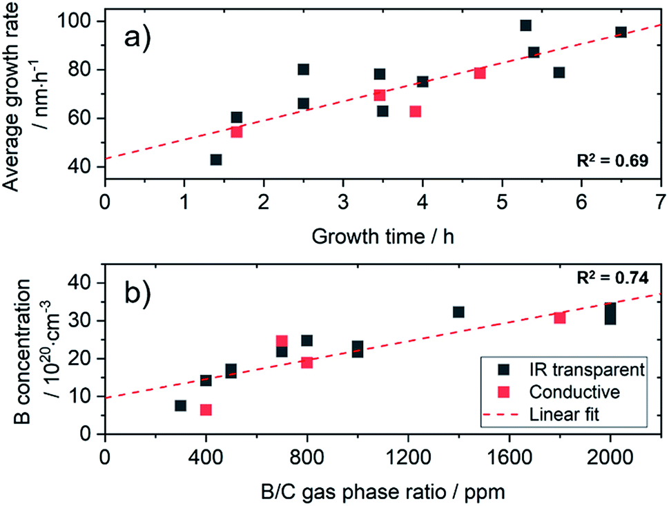 | ||
| Fig. 1 (a) Time dependence of the average growth rate for thin BDD layers (60–620 nm) and (b) resulting sample boron concentration in relation to the B/C gas phase concentration. (Data obtained from SIMS measurements). | ||
However, significant variations occur (R2 = 0.69), which make a fast and reliable characterisation mandatory. In our case, when using 4′′ wafers, constant growth rates are not obtained before a thickness of 2 μm, which corresponds to a growth time of approx. 24 h. Using a limited growth model, this can be fitted and enables reproducible growth of diamond films with a thickness above 1 μm with an error margin of less than 2% (Fig. S2†). Interestingly, in our experiments the amount of the dopant gas (TMB) did not show strong influence on the growth rate for these heavily doped diamond films (Fig. S3†). However, when changing conditions and dopant concentrations, this may be different.26
The total amount of B incorporated into the diamond lattice correlates with the amount of TMB in the gas phase (Fig. 1b), but variations for the thin layers can be expected (R2 = 0.74).
All grown diamond films used in this study and their characteristics are summarised in Table 1.
Characterisation
In order to assess the chemometric analysis for determining thickness and dopant concentration directly after synthesis of diamond films, the as-grown samples were used for all characterisation methods without further treatment. AFM measurements confirmed good crystallinity of the films as well as an increasing RMS roughness with increasing thickness as expected due to the continued growth of the single crystallites (Table 1, Fig. S1†). IR measurements confirmed low absorbance in a wide range from 5000 to 500 cm−1 (Fig. 2).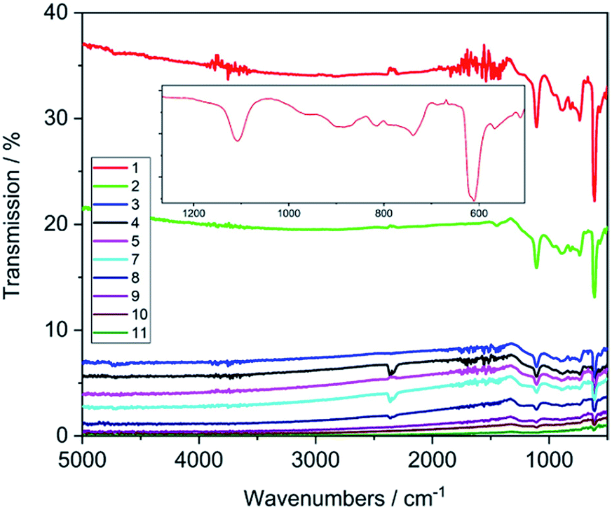 | ||
| Fig. 2 IR-transmission spectra of the synthesised diamond films. Inset shows a zoomed view of sample 1 in the fingerprint region. (C1–C4 samples are left out due to the conductive silicon substrate used for these films, which completely absorbs the IR). | ||
The transmission data is homogeneous over the whole measurement range and shows a strong dependence on the thickness of the diamond film. Plotting the absorbance of the films at 2750 cm−1vs. the thickness, a linear dependence can be clearly observed (Fig. S4†), which indicates that the change in conductivity induced by the different dopant concentration is not significant for the deposited diamond films.
In the recorded spectra only a few bands are visible originating from the silicon substrate (611, 738, 891 cm−1, phonon bands, 1085 cm−1, Si–O). Samples with conductive silicon substrates (C1–C4) completely absorbed the IR light (data not shown).
Raman characterisation on the diamond films was carried out at different locations of the samples using a laser wavelength of 532 nm. Only negligible variations were observed for the individual spectra recorded at the different spots of the same sample. Selected spectra from Table 1 are shown in Fig. 3a.
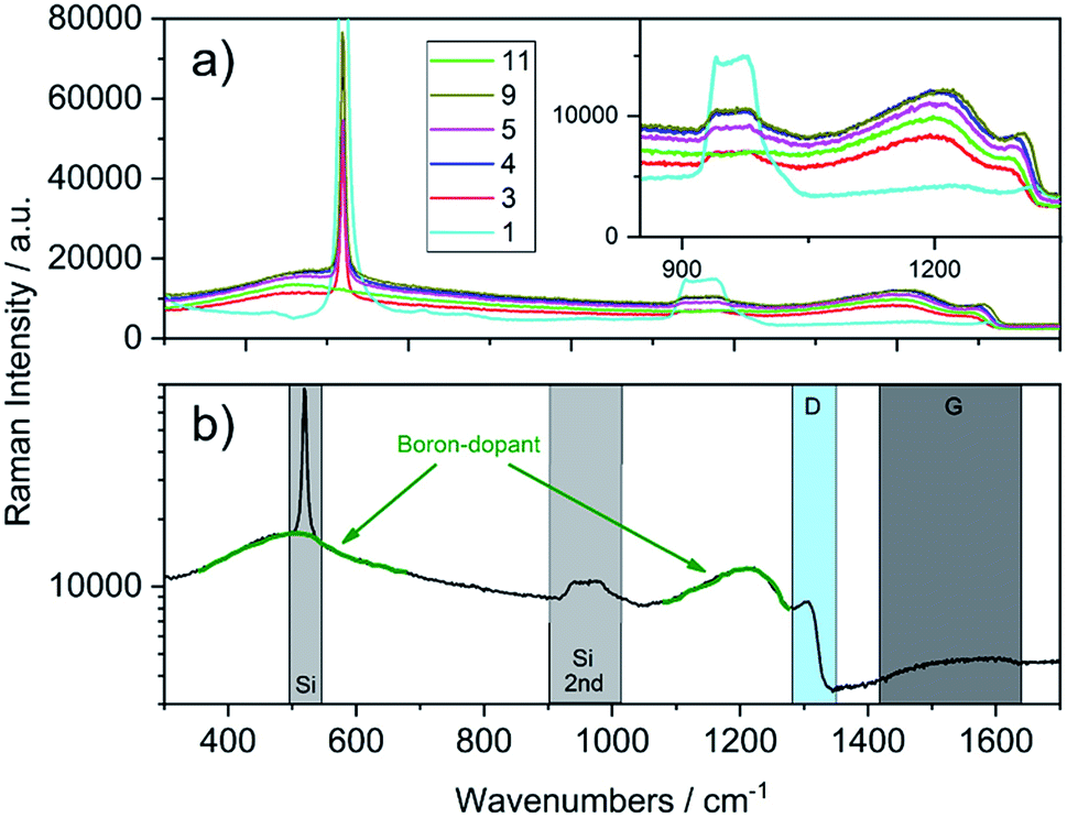 | ||
| Fig. 3 (a) Raman spectra recorded of the as-grown diamond films (inset shows the region of the diamond phonon line). (b) Single spectrum of the sample 7 (see Table 1, 300 nm, 16.2 × 10²⁰ B/cm−3) with highlighted regions for bands corresponding to silicon, diamond and boron-doping (note: intensity is plotted in logarithmic scale for better presentation). | ||
In contrast to the IR spectra, independent from the thickness, the traces are shifted to higher or lower intensity and both materials, silicon and BDD show characteristic bands. The single spectrum in Fig. 3b shows the regions of interest for the two materials. Silicon shows a sharp band at 520 cm−1 and a wide band from 920 to 1045 cm−1, which correspond to the one-phonon peak and the two-phonon overtone, respectively.27 The diamond single phonon line is located at 1332 cm−1; however, due to boron doping this line undergoes a Fano resonance, leading to a peak shift, a decrease in intensity and a broadening (D region in Fig. 3b). Apart from that, 2 wide bands at around 500 and 1200 cm−1 are observed, which can be assigned to boron-dimer vibrations and symmetry breaking of the diamond lattice.20 Additional information on the quality of the grown diamond is obtained from the region between 1400 and 1600 cm−1, where the G-band assigned to sp2-carbon impurities is observed. Depending on the thickness of the diamond film, the signals from the underlying silicon are different in intensity, decreasing with deposited film thickness.
For example, sample 11 with a thickness of 620 nm lacks bands from the underlying substrate. Using these spectra, the PLSR was carried out using the whole set of diamond films. Without taking the substrate resistivity into account, it was observed that the prediction of dopant concentration reaches a root mean square error of prediction (RMSEP) of 1.74 × 10²⁰ (six LVs according to variance captured). However, after including the substrate resistivity into the model, the prediction of boron concentration can be carried out with an RMSEP of 1.46 × 10²⁰. Fig. 4 shows the predicted values from the model plotted versus the obtained results from SIMS. From the randomly selected validation set, a RMSEP for the B concentration of 1.46 × 10²⁰ atoms per cm3 and 36.57 nm for the thickness are obtained. Table 2 summarises the results of the PLSR. According to that, from the characteristic features in the spectrum, the B concentration for these heavily doped films can be accurately predicted, in accordance with literature results.28
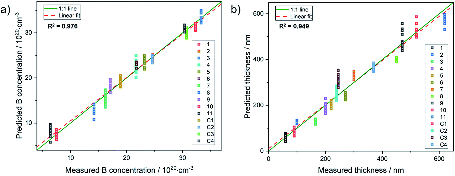 | ||
| Fig. 4 Results from PLSR: (a) measured concentration vs. predicted values from the chemometric model and (b), predicted thickness vs. measured values for the diamond films. | ||
| B concentration | Thickness | Substrate resistivity | |
|---|---|---|---|
| Without taking the substrate into account | |||
| R 2 | 0.961 | 0.950 | |
| RMSEC | 1.54 × 10²⁰ | 31.63 | |
| RMSECV | 1.63 × 10²⁰ | 34.62 | |
| RMSEP | 1.74 × 10²⁰ | 37.8 | |
|
|||
| Taking the substrate into account | |||
| R 2 | 0.976 | 0.949 | 0.869 |
| RMSEC | 1.16 × 10²⁰ | 32.26 | 1.77 |
| RMSECV | 1.42 × 10²⁰ | 34.52 | 2.39 |
| RMSEP | 1.46 × 10²⁰ | 36.57 | 2.12 |
However, for the film thickness where no characteristic peak is present, the resulting prediction accuracy is close to the mean value of the roughness RMS (30 nm) of the diamond film set and hence very close to the theoretical maximum.
Apart from that, taking the substrate into account, the model also predicts the resistivity with an accuracy of approx. 2 Ω. This can be used to determine the characteristic of the whole diamond-coated element.
Conclusions
In conclusion, we demonstrated a chemometric model, which is able to obtain boron concentration and thickness with high accuracy from Raman spectra, which reflects a significant advantage due to the short analysis times of a few seconds compared to other techniques such as SIMS. This analysis can be carried out on as-grown samples without further preparation steps. The characterisation method is non-destructive and non-invasive, leaving the diamond film unaltered for further processing. Thus, it is ideally suited for fast and automated characterisation of as-grown films after diamond synthesis, which is prone to variations in the early growth stages, i.e., for thin film growth. Additionally, substrate parameters can be included into the model to characterise a diamond-coated element as a whole. From this observation, we are confident that the described approach can be readily adapted to other materials, e.g. quartz,12 freestanding layers,13 or intrinsic diamond. Using Raman microscopy, also laterally resolved data on thickness and B concentration, e.g., for microstructured OTEs with thin BDD layers, can be obtained.Conflicts of interest
There are no conflicts to declare.Acknowledgements
The authors acknowledge financial support from the Baden-Württemberg Stiftung (Photokon) and the Federal Ministry of Education and Research (BMBF – PHOIBE: 13N13722). We thank T. Fuchs for assistance with SIMS measurements, D. Luick is thanked for her support with IR measurements, P. Krebs and M. Härtelt for helpful discussion.Notes and references
- S. E. Coe and R. S. Sussmann, Diamond Relat. Mater., 2000, 9, 1726–1729 CrossRef CAS.
- M. Füner, C. Wild and P. Koidl, Appl. Phys. Lett., 1998, 72, 1149–1151 CrossRef.
- J.-P. Lagrange, A. Deneuville and E. Gheeraert, Diamond Relat. Mater., 1998, 7, 1390–1393 CrossRef CAS.
- J. V. Macpherson, Phys. Chem. Chem. Phys., 2015, 17, 2935–2949 RSC.
- V. Bezerra dos Santos, E. L. Fava, O. D. Pessoa-Neto, S. R. Bianchi, R. C. Faria and O. Fatibello-Filho, Anal. Methods, 2014, 6, 8526–8534 RSC.
- S. Fierro, N. Mitani, C. Comninellis and Y. Einaga, Phys. Chem. Chem. Phys., 2011, 13, 16795 RSC.
- N. Ikemiya, K. Natsui, K. Nakata and Y. Einaga, ACS Sustainable Chem. Eng., 2018, 6, 8108–8112 CrossRef CAS.
- J. H. T. Luong, K. B. Male and J. D. Glennon, Analyst, 2009, 134, 1965 RSC.
- R. Bogdanowicz, A. Fabiańska, L. Golunski, M. Sobaszek, M. Gnyba, J. Ryl, K. Darowicki, T. Ossowski, S. D. Janssens, K. Haenen and E. M. Siedlecka, Diamond Relat. Mater., 2013, 39, 122–127 CrossRef.
- K. Cinková, K. Kianičková, D. M. Stanković, M. Vojs, M. Marton and L. Švorc, Anal. Methods, 2018, 10, 991–996 RSC.
- T. Chen, T. Ma and R. C. Barker, Appl. Phys. Lett., 1983, 43, 901–903 CrossRef CAS.
- J. Stotter, J. Zak, Z. Behler, Y. Show and G. M. Swain, Anal. Chem., 2002, 74, 5924–5930 CrossRef CAS PubMed.
- S. Haymond, J. K. Zak, Y. Show, J. E. Butler, G. T. Babcock and G. M. Swain, Anal. Chim. Acta, 2003, 500, 137–144 CrossRef CAS.
- D. Neubauer, J. Scharpf, A. Pasquarelli, B. Mizaikoff and C. Kranz, Analyst, 2013, 138, 6746 RSC.
- T. Yoshikawa, F. Gao, V. Zuerbig, C. Giese, C. E. Nebel, O. Ambacher and V. Lebedev, Diamond Relat. Mater., 2016, 63, 103–107 CrossRef CAS.
- M. A. Pinault-Thaury, F. Jomard, C. Mer-Calfati, N. Tranchant, M. Pomorski, P. Bergonzo and J. C. Arnault, Appl. Surf. Sci., 2017, 410, 464–469 CrossRef CAS.
- H. Kawarada, Y. Yokota, Y. Mori, K. Nishimura and A. Hiraki, J. Appl. Phys., 1990, 67, 983–989 CrossRef CAS.
- O. Almora, C. Aranda, E. Mas-Marzá and G. Garcia-Belmonte, Appl. Phys. Lett., 2016, 109, 173903 CrossRef.
- R. Locher, J. Wagner, F. Fuchs, M. Maier, P. Gonon and P. Koidl, Diamond Relat. Mater., 1995, 4, 678–683 CrossRef CAS.
- A. N. Utyuzh, Y. A. Timofeev and A. V. Rakhmanina, Inorg. Mater., 2004, 40, 926–931 CrossRef CAS.
- R. G. Brereton, Chemometrics, John Wiley & Sons, Ltd, Chichester, UK, 2003 Search PubMed.
- P. Geladi and B. R. Kowalski, Anal. Chim. Acta, 1986, 185, 1–17 CrossRef CAS.
- J. A. Cornell, Experiments with Mixtures, John Wiley & Sons, Inc., Hoboken, NJ, USA, 2002, vol. 185 Search PubMed.
- T. Yoshikawa, V. Zuerbig, F. Gao, R. Hoffmann, C. E. Nebel, O. Ambacher and V. Lebedev, Langmuir, 2015, 31, 5319–5325 CrossRef CAS PubMed.
- J. Hees, A. Kriele and O. A. Williams, Chem. Phys. Lett., 2011, 509, 12–15 CrossRef CAS.
- Y. Zou and K. Larsson, J. Phys. Chem. C, 2016, 120, 10658–10666 CrossRef CAS.
- K. Uchinokura, T. Sekine and E. Matsuura, Solid State Commun., 1972, 11, 47–49 CrossRef CAS.
- P. W. May, W. J. Ludlow, M. Hannaway, P. J. Heard, J. A. Smith and K. N. Rosser, Diamond Relat. Mater., 2008, 17, 105–117 CrossRef CAS.
Footnote |
| † Electronic supplementary information (ESI) available. See DOI: 10.1039/c8ay02468e |
| This journal is © The Royal Society of Chemistry 2019 |