
 Open Access Article
 This Open Access Article is licensed under a Creative Commons Attribution-Non Commercial 3.0 Unported Licence
Chemical imaging of human teeth by a time-resolved Raman spectrometer based on a CMOS single-photon avalanche diode line sensor
Jere
Kekkonen
 *a,
Mikko A. J.
Finnilä
b,
Jarkko
Heikkilä
c,
Vuokko
Anttonen
cd and
Ilkka
Nissinen
a
*a,
Mikko A. J.
Finnilä
b,
Jarkko
Heikkilä
c,
Vuokko
Anttonen
cd and
Ilkka
Nissinen
a
aCircuits and Systems Research Unit, University of Oulu, 90014 Oulu, Finland. E-mail: jere.kekkonen@oulu.fi; ilkka.nissinen@oulu.fi
bResearch Unit of Medical Imaging, Physics and Technology, University of Oulu, 90220 Oulu, Finland. E-mail: mikko.finnila@oulu.fi
cDepartment of Cariology, Endodontology and Pediatric Dentistry, University of Oulu, 90220 Oulu, Finland. E-mail: vuokko.anttonen@oulu.fi; jarkko.heikkila@student.oulu.fi
dMedical Research Center, Oulu University Hospital and University of Oulu, 90220 Oulu, Finland. E-mail: vuokko.anttonen@oulu.fi
First published on 12th September 2019
Abstract
Raman spectroscopy is a powerful analytical tool to be used in many biomedical applications and could be potentially translated into clinical work. The challenge of Raman spectroscopy in biomedical applications is the high inherent fluorescence of biological samples. One promising method to suppress the fluorescence background is to use pulsed lasers and time-gated detectors but the complexity of time-gated systems has hindered their widespread usage. We present here chemical imaging of human teeth by means of a new kind of compact and practical fluorescence-suppressed Raman spectrometer based on a time-resolved 16 × 256 CMOS single-photon avalanche diode (SPAD) line sensor with an integrated 256-channel 3-bit on-chip time-to-digital converter. The chemical images were constructed by utilizing a simple unsupervised machine learning algorithm (k-means clustering). The high quality of Raman spectra measured with the time-resolved CMOS SPAD-based Raman spectrometer was verified by comparing the spectra to those collected with a commercial conventional continuous wave (CW) Raman spectrometer. The spectra measured by using the time-resolved CMOS SPAD-based Raman spectrometer had 4.4–8.8 times higher signal to peak-to-peak noise ratio values than the spectra from the CW Raman spectrometer when the same radiant exposure (∼300 J mm−2) was used with both spectrometers. This paper shows in practice the potential of time-resolved CMOS SPAD-based Raman spectroscopy in the field of biomedicine and we expect that the presented technology could pave the way for the development of new kind of compact and practical fluorescence-suppressed Raman spectrometers to be used both in biomedical research and clinical settings.
Introduction
The condition of our teeth does not only indicate the state of our oral health, but it also can offer information on other health issues such as diabetes history, cardiovascular disease, renal insufficiency and even neurobehavioral functioning.1–4 Therefore, the tooth structure and chemistry has been studied extensively with various techniques such as synchrotron microprobe X-ray fluorescence, particle-induced X-ray emission (PIXE), secondary ion mass spectrometry (SIMS) and microcomputer tomography.4–7 These complex and expensive techniques are mainly used in basic research and not in clinical practice. However, the recent advancements in laser and optical engineering have enlarged dentists’ clinical toolboxes with, for example, the novel light-emitting diode and laser fluorescence-based devices to analyse the condition and chemical changes of teeth.8 Another very promising and powerful optical tool to characterizes tooth tissues is Raman spectroscopy.9 Besides dentistry, Raman spectroscopy has shown its potential in many other biomedical applications since it can nondestructively and quantitively resolve the chemical and molecular composition of a sample or even biochemical changes in cells, tissues and body fluids.10 This may reveal novel biomarkers with diagnostic or even prognostic value in clinical use. In dentistry, Raman spectroscopy has been used in the early detection and characterization of dental caries, analysis of fluorosis-affected teeth and chemical profiling of adhesive/caries-affected dentin interface, for example.11–15 Raman spectroscopy have major advantages over other optical spectroscopy techniques, such as IR spectroscopy, when considering biological specimens. These include minimal sample preparation and the weak Raman interference with water.10,16 In addition, compared to the more conventional dentistry research and medical imaging modalities, such as PIXE, SIMS, computed tomography and magnetic resonance imaging, the advantage of Raman spectroscopy is the capability to provide accurate chemical images and near real-time molecular information with a lower cost.16,17Besides the many advantages, Raman spectroscopy has its own drawbacks that have hampered the technique to show its full potential in dentistry and overall in the biomedical field. The first one is the faint nature of Raman signal since approximately one in every 108 of the incident photons gets shifted from its original frequency due to Raman scattering.18 Thus, a great effort has been made over the past decades to improve the Raman instrumentation and analysis methods to exploit the faint Raman signal.19 Despite the advancements made, long signal acquisition times might be still required in some cases to compensate for the insufficient signal-to-noise ratio (SNR) leading to an unacceptable measurement time in a clinical setting. Another big factor reducing the SNR of the Raman signal is the high fluorescence background of biological samples that can partly or even totally mask the weaker Raman signal. Fluorescence emission can be considered as a competing phenomenon for the Raman scattering because it does not contain as detailed information on the molecular structure of a sample as Raman scattering does. Strong fluorescence background causes also problems in Raman analyses of teeth, especially when caries-affected teeth are measured.12,20–22 A commonly used method to suppress the problematic fluorescence background both generally and specifically in Raman analyses of teeth is to use longer excitation wavelengths in the near-infrared region of the electromagnetic spectrum.12,20,23 The disadvantage of this technique is that also the already faint Raman signal weakens to the fourth power of the wavelength and thus, the SNR tends to stay low, especially when highly fluorescent samples, such as caries-affected teeth, are measured.20,24 Another common method is to photobleach the samples for several seconds or even minutes before the acquisition of the spectral data but the obvious problem of this technique is its time-consuming nature.22
One very promising method to suppress the fluorescence background without weakening the Raman signal or increasing the measurement time is based on the time response difference between the Raman scattering and fluorescence emission. The Raman scattering is an instant process whereas a typical lifetime of fluorescence emission is around 10 ns.18,25 Therefore, the fluorescence background can be suppressed by illuminating the sample by a short-pulsed laser instead of conventional continuous wave (CW) laser and by enabling the collection of the photons from the sample only during the laser pulses by means of a time-gated detector as depicted in Fig. 1. The fluorescence suppression obtained by this time gating technique is approximately proportional to the ratio between the time gate width and the fluorescence lifetime of the sample.24 Thus, the widths of the laser pulse and time gate should be in the sub-nanosecond range to gain meaningful fluorescence suppression (a factor of 10 or more) when samples having nanosecond-scale fluorescence lifetimes are measured. Two examples of commonly used techniques to implement time-gated detectors are ultra-fast gated charge-coupled devices (ICCDs) and Kerr gates with detectors.21,26,27 The disadvantages of these techniques are that they are complex, expensive and not portable, which have hindered their widespread use and clinical implementation and restricted their use mainly into research laboratories.
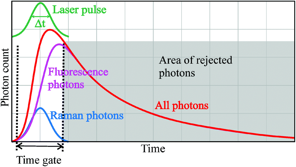 | ||
| Fig. 1 Time distributions of a laser pulse, fluorescence emission and Raman scattering and principle of fluorescence suppression by means of time gating. | ||
A recently proposed solution for the restricting challenges of time gating techniques is to use time-gated single-photon avalanche diodes (SPADs) fabricated in complementary-metal–oxide-semiconductor (CMOS) technology as the detector of a fluorescence-suppressed Raman spectrometer.28,29 SPADs are suitable for Raman spectroscopy because they can digitally detect single photons. The principle of SPAD-based Raman spectroscopy is the same as in any other time-correlated single-photon counting (TCSPC) measurement when the photon detection probability is markedly less than one as it is in Raman spectroscopy.30 Advantages of CMOS SPAD-based sensors include that SPADs can be time-gated to the photon detection mode only during the laser pulse more easily compared to ICCDs, for instance. In addition, time gate width short as 50 ps has been already achieved with CMOS technology.31 CMOS technology makes it also possible to integrate all the necessary TCSPC electronics into a single integrated circuit with a SPAD array further reducing the size and complexity of the whole device.31–35 Time-correlated CMOS SPAD detector circuits are also mass producible and thus cost-effective. All these benefits of CMOS SPAD-based Raman spectroscopy are favourable when the translation of the technique to clinics is considered since the clinical implementation is influenced by practical, logistical and financial factors. Furthermore, time-resolved CMOS SPAD sensors enable to implement novel functionalities for Raman spectroscopy, such as Raman radar and Raman depth-profiling operations, in a practical and compact way, which might in the future open novel application possibilities for Raman spectroscopy in various fields of science.36,37
In this paper, we demonstrate the capability of a fluorescence-suppressed Raman spectrometer based on a time-resolved 16 × 256 CMOS SPAD line sensor with an integrated 256-channel 3-bit on-chip time-to-digital converter (TDC)31 to form chemical images of extracted human teeth. This is the first time, to the best of our knowledge, that CMOS SPAD-based Raman spectroscopy is used to chemically image human teeth. The chemical images are constructed by using a simple unsupervised machine learning algorithm (k-means clustering) to classify the spectral data based on several Raman peak intensity ratios. The tooth samples are also analysed by using a commercially available conventional CW Raman spectrometer with the same radiant exposure as a reference method to show the advantages of the developed time-resolved CMOS SPAD-based Raman spectrometer.
Experimental
Tooth samples
A Finnish law on medical use of human organs, tissues and cells (Finlex §20) declares that tissue samples taken to detect or treat a disease or to detect the cause for death, can be donated and used in medical research, development of methods, quality control and teaching with the consent of the unit responsible for getting the sample, if in donation or use no personal identifications are used. The teeth in this study had been extracted from public health care patients in the City of Oulu, Finland, to treat dental caries, periodontitis or pericoronitis. After extraction, the teeth were donated to the University of Oulu for research and education by officers of the City of Oulu. The identity of patients cannot be tracked in any case and informed consent was obtained from all human subjects.In total, three tooth samples (labelled from now on as tooth 1–3, see Fig. 4(a–c)) were included into this proof-of-concept study to investigate the potential of time-resolved CMOS SPAD-based Raman spectroscopy in dentistry applications. The roots of the teeth were removed so that the cut surface was located apically from the enamel-cement junction. After this, the crown was cut in two halves using a sample saw suitable for this purpose (IsoMet Low Speed, Buehler, Illinois, USA) The more suitable half was chosen for Raman analysis. The selected crown halves were cast in metallurgical resin (Buehler, EpoThin 2, Illinois, USA) with minimal tissue penetration and low peak temperature. Measurements surface were polished by first grinding with sandpapers by successively reducing grades and finally polished with suspension of 0.05 mm γ-alumina slurry (MetPrep Ltd, Coventry, UK). One crown half (tooth 3) was analysed without the resin cast.
Measurement setups
A block diagram of the developed time-resolving CMOS SPAD-based Raman spectrometer and its principled timing diagram are shown in Fig. 2(a) and (b), respectively. The excitation source of the spectrometer is a pulsed laser (Teem Photonics, Meylan, France, model ANG-500P-CHS) that has a wavelength, bandwidth, pulse width (full width at half maximum), pulse energy and pulse rate of 532 nm, 0.11 nm, 160 ps, 0.5 μJ and 350 kHz, respectively. A small portion of the laser pulses is guided to an optical detector by means of a beam splitter. The optical detector, which is coupled with a comparator, generates a logic level trigger signal that is passed through an off-chip digital delay unit to the 16 × 256 CMOS SPAD line sensor in order to bias the SPADs to the Geiger mode synchronously with the laser pulse (trigger and bias signals in Fig. 2(a)). The line sensor has an integrated 256-channel 3-bit on-chip TDC (one channel per spectral point) to measure the time-of-arrivals of backscattered Raman photons (reflectance configuration with zero source-to-detector distance).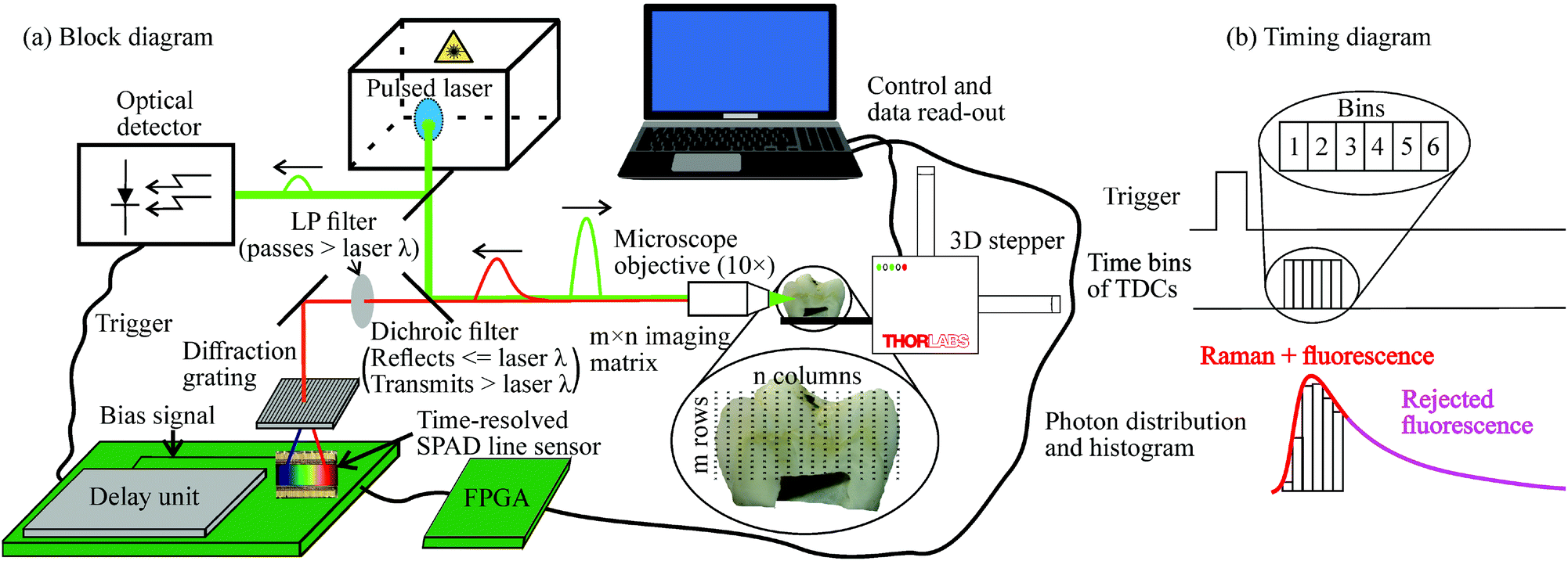 | ||
| Fig. 2 (a) A block diagram of the time-resolving Raman spectrometer based on a 16 × 256 CMOS SPAD line sensor with an integrated 256-channel 3-bit on-chip time-to-digital converter and (b) its principled timing diagram. The bias signal of the bins 1–6, i.e. of the time gate, can be delayed with the delay unit to synchronize the electrical and optical signals of the system enabling the photon collection only during the time when the Raman echo pulse from the sample reaches the detector to gain efficient fluorescence suppression. | ||
The histogram shown in Fig. 2(b) starts to form after several thousand laser pulses have been shot to the sample. The bins of the TDC numbered as 1–6 are stabilized by a reference-locked delay line resulting in a bin size of ∼100 ps and thus the total time gate width of ∼600 ps. The bias signal of the bins 1–6 can be delayed with the digital delay unit to synchronize the electrical and optical signals of the system enabling the photon collection only during the time when the Raman echo pulse from the sample reaches the detector. In other words, this means that the time gate (bins 1–6) collect all the backscattered Raman photons from the sample but only a small part of the total fluorescence emission and other background radiation caused by ambient light resulting in effective fluorescence and background suppressions as depicted in Fig. 2(b). In addition, there is a longer unstabilized bin 0, which is used to collect the background photons arriving before the Raman pulse and to help to adjust the timing of the actual time gate (bins 1–6), and an overrange bin 7, which detects the SPAD quenching signal generated by the CMOS logic to end an ongoing measurement cycle.
Majority of the laser pulse energy is guided through a microscope objective (Olympus Plan N, 10×/0.25 NA, spot size after objective ∼150 μm) to illuminate the sample that is placed on a sample holder connected to a 3D stepper motor to enable the scanning of the sample in XY-plane. Backscattered photons from the sample are guided through a dichroic and a longpass filters, which block the Rayleigh scattered photons (filters transmit only wavelengths longer than the laser wavelength), and a diffraction grating to the CMOS SPAD line sensor. The diffraction grating diverges the incoming photons so that the position of each SPAD row corresponds to a specific range of wavenumbers. The line sensor has a pitch of 35.2 μm and thus a wavenumber resolution of ∼6 cm−1. The controlling of the detector electronics and the data read-out from the detector chip was done by using a field-programmable gate array control circuit (FPGA in Fig. 2) connected to a computer.
All the data post-processing was done by using custom MATLAB scripts. Data post-processing included removal of the dark count noise of the SPADs, correction of the nonidealities of the SPAD line sensor (including filtering by a mean filter with a window size of 2) and compensation for the residual fluorescence within the time gate by a method earlier described by Nissinen et al.31 In addition, from the spectra of the teeth samples cast in resin were subtracted a reference spectrum of resin to compensate for the effects of resin on the spectra of the tooth samples. The spectral accuracy of the sensor has been shown to be within the spectral resolution (∼6 cm−1) with various standard Raman samples, such as 50/50 mixture of toluene/acetonitrile, TiO2 and ethanol.31,36,37 A detailed description of the 16 × 256 CMOS SPAD sensor with the integrated 256-channel 3-bit on-chip TDC is given in the article by Nissinen et al.31
The reference Raman set-up was a commercial confocal CW Raman imaging microscope (Thermo Fisher Scientific, USA, model DXR™2xi) equipped with a 10× objective (Olympus Plan N, 10×/0.25 NA). The CW laser of the reference spectrometer has a wavelength, average power and spot size of 532 nm (same as used with the time-resolved CMOS SPAD-based Raman spectrometer), 10 mW and 2.6 μm, respectively. The wavenumber resolution of the CW Raman spectrometer was 2 cm−1. The post-processing of the spectra measured by means of the CW Raman spectrometer was also performed by using custom MATLAB scripts, including baseline correction (polynomial curve fitting) and filtering of the data (mean filtering with the window size of 10).
Scanning of the tooth samples
The tooth samples were scanned in XY-plane in the measurements conducted by using the time-resolved CMOS SPAD-based Raman spectrometer to be able to form the 2D chemical images of the samples. The step size of the scanning both in X and Y direction was 250 μm. The imaging area and thus, the number of columns and rows in the imaging matrix varied between the samples so that the total number of pixels in the matrixes varied from 738 to 770. At each pixel, 10 million laser pulses were shot to the sample resulting in acquisition time of ∼29 s per pixel with the laser repetition rate of 350 kHz and thus, the overall scanning time varied from 5 h 57 min to 6 h 12 min (plus the short time that it takes to move the sample between two subsequent pixels).The reference spectra measured with the CW Raman spectrometer were collected only from selected pixel matching with the clustering results. The acquisition time for the reference Raman spectra was set to 0.17 s (6 Hz) in order to have about the same radiant exposure per a pixel as with the time-resolved Raman spectrometer to be able to compare the performance of the spectrometers. These high radiant exposures are still safe to use but a further rise of the exposure would have caused a risk to damage the samples. It should be also noted that the use of the same radiant exposure values with different laser spot sizes results in a different number of photons shot to the samples having further impact on the number of backscattered photons (both the Raman and fluorescence photons) and thus, on the shot noise SNR. In addition, other issues, such as the efficiency of the optical paths (both the excitation and collection sides), also affect the shot noise SNR making the equal comparison between the different sensor technologies a major challenge. Keeping all these issues in mind, we decided to use signal to peak-to-peak noise ratio (SNRpp) instead of the common shot noise SNR to define the spectral quality. Besides, the peak-to-peak noise in the time-resolved SPAD line sensor is not dominated by the shot noise but by the distortion caused by the timing inhomogeneities and other sensor non-idealities.31 This distortion is directly proportional to the number of shot photons meaning that number of shot photons does not have a direct impact to the SNRpp values with the time-resolved Raman setup.
Formation of the chemical images of the tooth samples
A Raman spectrum of a cross-sectioned sound dentin measured by using the time-resolved CMOS SPAD-based Raman spectrometer is shown in Fig. 3, which also shows the Raman assignments of sound dentin. At first, several Raman peak intensity ratios were computed and these intensity ratios were PO4(ν1) to amide III, PO4(ν1) to amide I, PO4(ν1) to CH2 and PO4(ν1) to PO4(ν2). These ratios were selected because they reflect crystallinity and mineralization of the tooth samples.9 These ratios alongside with the residual fluorescence intensity within the 600 ps time gate were used as the input data (5 × 1 column vector) when the pixels were clustered depending on the tooth sample either to four or five chemically different groups. The residual fluorescence intensity was determined from the data to which only the dark count noise removal was applied. In addition, the residual fluorescence intensity was weighted by a factor of nine in the clustering to increase the effect of fluorescence intensity because only the residual fluorescence emission within the 600 ps time gate was captured. The chemical characteristics of different clusters are discussed alongside the resulted chemical images in the Results & discussion section. | ||
| Fig. 3 Raman spectrum of a cross-sectioned sound dentin measured with the time-resolved CMOS SPAD-based Raman spectrometer. The Raman assignments are taken from articles by Carden et al.39 and Pascart et al.40 | ||
We used k-means clustering, which is a simple unsupervised machine learning algorithm, for identifying chemically similar areas.38 In a nutshell, the k-means clustering can be divided into five steps: 1. Number (k) of clusters and initial cluster centres are defined (normally in the k-means algorithm the initial cluster centres are chosen randomly but here they were selected knowingly) 2. The distance (i.e. difference) of each pixel to the cluster centres is computed 3. The pixels are clustered into clusters to which their distance is the smallest 4. The cluster centres are recomputed 5. The second and third steps are done again and if the optimal clustering is not achieved, i.e. the assignments of the pixels to the clusters still change, the cluster centres are recomputed, and the algorithm is repeated starting from the second step. The distance of the pixels in the clustering was quantified by using the city block distance (aka taxicab geometry, Manhattan distance and L1 distance), which is the sum of absolute differences between the corresponding elements in two column vectors, i.e. between the elements in a cluster centre column vector (the different Raman peak ratios of the cluster centre) and the elements in an input column vector (the different Raman peak ratios at a certain pixel). The used distance metric was chosen instead of more commonly used distance metrics, such as the cosine distance, simply because it offered better clustering results and thus better chemical images for this kind of input data (column vectors consisting of Raman peak ratios).
Results & discussion
Chemical images of human teeth constructed by using the time-resolved CMOS SPAD-based Raman spectrometer and k-means clustering algorithm
Photographs of the tooth samples and their chemical images constructed by using the time-resolved CMOS SPAD-based Raman spectrometer and k-means clustering algorithm are shown in Fig. 4(a–c) and (d–f), respectively. In total, five chemically different clusters (plus one overrange cluster) were identified from the three tooth samples and example spectra from the areas covered by these clusters are shown in Fig. 6(a–e). The example spectra of clusters 1–4 are from tooth 1 and the example spectrum of cluster 5 is from tooth 2. The average Raman peak ratios used in the clustering are shown in Table 1. | ||
| Fig. 4 (a–c) Photographs of the tooth samples and (d–f) their chemical images constructed by using the time-resolved CMOS SAPD-based Raman spectrometer and k-means clustering algorithm. The numbers indicate the different clusters. | ||
| Cluster | Fluor. Int (a.u.) | PO4(ν1) | PO4(ν1) | PO4(ν1) | PO4(ν1) |
|---|---|---|---|---|---|
| PO4(ν2) | CH2 | Amide I | Amide III | ||
| Cluster 1 (enamel) | 0.021 | 6.54 | NaN | NaN | NaN |
| Cluster 2 (DEJ) | 0.016 | 6.40 | 16.33 | 10.84 | 27.63 |
| Cluster 3 (dentin I) | 0.009 | 6.11 | 8.93 | 7.36 | 14.93 |
| Cluster 4 (dentin II) | 0.010 | 6.27 | 8.60 | 5.98 | 12.82 |
| Cluster 5 (caries) | 0.035 | 7.17 | NaN | NaN | NaN |
Cluster 1 represents sound tooth enamel and its main characteristics that separate it from the other clusters are the high intensity of phosphate peaks and the lack of the CH2 and amide I and III peaks. This is because the enamel tissue is highly mineralized (almost 100%) hydroxyapatite (Ca10(PO4)6(OH)2) and the cluster represents healthy tissue sample. Cluster 2 represents the transition area between the dentin and enamel containing the dentino-enamel junction (DEJ) transition zone although the borderline of this cluster in tooth 2 is not as strict as with the teeth 1 and 3.41 The main characteristics of this cluster that separate it from clusters 1 (sound enamel), 3 and 4 (sound dentin I and II) are the fluorescence intensity and the higher PO4(ν1) to CH2 and PO4(ν1) to amide I and III ratios as shown in Table 1. These results are explained by the fact that the enamel is mineralized hydroxyapatite whereas mineral content of dentine is approximately 70% (weight) or 45% (volume), when the rest is mainly type I collagen (90%). In addition, the characteristics of cluster 2 (DEJ) could be partly explained by the possible partial volume artefact caused by the laser beam illuminating both the areas of the enamel and dentin at the same time (spot size ∼150 μm).
As already mentioned, both clusters 3 and 4 represent sound dentin and the characteristics separating them from clusters 1 (sound enamel) and 2 (DEJ) are the PO4(ν1) to CH2 and PO4(ν1) to amide I and III ratios. The main differences between the sound dentin clusters 3 and 4 is that the fluorescence intensity in cluster 4 (sound dentin II) is higher than in cluster 3 (sound dentin I) and the PO4(ν1) to CH2 and PO4(ν1) to amide I and III ratios are lower in cluster 4 (sound dentin II) than in cluster 3 (sound dentin I). The main reason why these ratios are lower in cluster 4 (sound dentin II) is that the intensity of PO4(ν1) peak is lower in cluster 4 (sound dentin II) than in cluster 3 (sound dentin I) indicating lower concentration of mineralized hydroxyapatite in cluster 4 (sound dentin II) than in cluster 3 (sound dentin I) and thus, lower mineral to organic ratio. Despite these differences between clusters 3 and 4 (sound dentin I and II), both of them were classified as clinically sound dentin by an experienced dentist.
The characteristics of clusters 1–3 are similar for all the tooth samples. The cluster 4 (sound dentin II) was identified only from tooth 1. Besides the clusters 1–4, two more clusters that were not present in tooth 1 were identified from teeth 2 and 3. Cluster 5 mainly represent caries-affected enamel (caries verified by a dentist with expertise and years of experience in caries detection and assessment) and the main characteristic separating it from the other clusters is the high fluorescence intensity, which is a commonly used marker to detect carries-affected dental tissue.8 Another characteristic feature of this cluster is the higher PO4(ν1) to PO4(ν2) ratio compared to the other clusters. Because the caries-affected areas are mainly located in enamel, the cluster 5 (caries-affected enamel) is also missing the CH2 and amide I and III peaks. It appears that even initial caries lesions cause changes in the composition of a tooth, which can be detected in Raman signatures.
Lastly, cluster 6 is just an overrange cluster that was used to identify the situations where the scanning went over the borderlines of a sample. The obvious characteristic of this background clusters is that it is missing all the spectral features of tooth tissue.
Comparison of Raman spectra measured by using the time-resolved CMOS SPAD-based Raman spectrometer and commercial reference CW Raman spectrometer
Example raw Raman spectra (i.e. spectra without any post-processing, such as dark count correction and filtering) of sound dentin (cluster 3) measured both with the time-resolved Raman spectrometer and CW reference Raman spectrometer with about the same radiant exposures (∼300 J mm−2) are shown in Fig. 5(a) and (b), respectively. These figures demonstrate the effectiveness of the fluorescence rejection achieved with the time-resolved Raman spectrometer. In addition, Fig. 5(a) shows the sawtooth-like distortion of the spectra caused by the timing inhomogeneities of the time-resolved SPAD line sensor. | ||
| Fig. 5 Example Raw Raman spectra of sound dentin (cluster 3) measured with (a) time-resolved CMOS SPAD-based Raman spectrometer and (b) commercial reference CW Raman spectrometer with about the same radiant exposures (300 J mm−2). | ||
Example post-processed Raman spectra of clusters 1–5 measured with both the time-resolved CMOS SAPD-based Raman spectrometer and commercial reference CW Raman spectrometer are shown in Fig. 6(a–e) and in Fig. 6(d–f). In Fig. 6(a–f) is also marked the SNRpp of each example Raman spectrum. The SNRpp here indicates the ratio between the Raman signal at 953 cm−1 (the highest Raman peak, PO4(ν1)) and the computed peak-to-peak noise amplitude. The peak-to-peak noise amplitude was calculated from the root mean square noise by first computing baseline corrected standard deviation (σ) for a short part of the measured signal without Raman peaks (wavenumber range ∼720–800 cm−1) and then multiplying the σ by six in order the cover 99.7% of the whole signal (assuming that the noise is normally distributed).
 | ||
| Fig. 6 Example post-processed Raman spectra from the areas covered by clusters 1–5 measured with (a–e) time-resolved CMOS SPAD-based Raman spectrometer (TR Raman) and (f–i) commercial reference CW Raman spectrometer (CW Raman). The radiant exposure was about the same (∼300 J mm−2) with both Raman spectrometer setups and the SNRpp indicates the ratio between Raman signal at 953 cm−1 and computed peak-to-peak noise amplitude (see text for details). The intensity of each spectrum was normalized by its maximum value to make the spectra more comparable. | ||
As can be seen from the spectra and SNRpp values in Fig. 6(a–f), the spectra measured by using the time-resolved CMOS SPAD-based Raman spectrometer have significantly less noise and thus 4.4–8.8 times higher SNRpp values (depending on measurement location in tooth cross sections) than the spectra measured by using the commercial reference CW Raman spectrometer. The noise in the example Raman spectra of clusters 2, 4 and 5 (DEJ, sound dentin 2 and carries-affected enamel) measured by using the CW Raman spectrometer is so high that it might decrease the reliability to derive the different Raman peak ratios for clustering and thus, also decrease the reliability of the clustering when this radiant exposure is used. The higher noise in the spectra measured by using the CW Raman spectrometer results from that in the CW Raman spectroscopy, besides the Raman photons also all the fluorescence photons are collected and thus, the Raman signal is masked by the fluorescence background decreasing the SNRpp. The SNRpp behaves similarly in the example spectra measured both by CW Raman spectrometer and time-resolved CMOS SPAD-based Raman spectrometer. The SNRpp is the highest in the example spectra measured from the sound enamel and the lowest in the example spectra measured from the carries-affected tissue and this finding is in line with the earlier studies.9 The window sizes used in the filtering of the CW and time-resolved data were different (10 vs. 2 adjacent spectral points, respectively) and this has a direct effect on the noise suppression, but the mean filtering has also effect on the signal amplitude and thus, the window size difference does not have a significant effect on the observed SNRpp differences (window sizes were selected so that the best possible SNRpp values could be reached with both datasets). All in all, the results of this section show the advantages of time-resolved CMOS SPAD-based Raman spectrometer over the commercially available CW Raman spectrometer when about the same radiant exposure is used with both spectrometers.
On the other hand, the acquisition time for a single spectrum with the reference CW Raman spectrometer was significantly shorter than the acquisition time with the time-resolved CMOS SPAD-based Raman spectrometer (0.17 s vs. 29 s) in order to obtain about the same radiant exposure values with both Raman spectrometers and the main reason for this shorter acquisition time was the smaller laser spot size (2.6 μm vs. 150 μm). The SNRpp of the spectra measured by using the reference CW Raman spectrometer could have been easily increased by increasing the acquisition time and thus, the number of photons shot to the samples, but this would also have increased the radiant exposure and caused a risk to damage the samples. Likewise, the acquisition time for a single spectrum measured by using the time-resolved CMOS SPAD-based Raman spectrometer could have been decreased, or the SNRpp of the spectra increased, by design the optical paths so that a smaller spot size could be used efficiently (both the efficiencies of the excitation and collection sides must be considered). Downside of using a small laser spot is that the excitation intensity (power transferred per unit area) might get too high, especially in the case of pulsed laser due to high peak powers, causing damages to biological tissues or other sensitive materials. Moderate decreasing of the acquisition time in the measurement conducted by using the time-resolved CMOS SPAD-based Raman spectrometer probably would have not caused significant decrease of the SNRpp because the main noise source with these signal levels (both Raman and fluorescence background) is not the shot noise but in fact the noise caused by the timing inhomogeneities, such as the timing skew, of the CMOS SPAD line sensor and this noise is not so strongly dependent on the acquisition time (i.e. on the number of shot photons) as the shot noise is.31 Therefore, the reduction of these nonidealities is obviously one of the main issues in the further development of the sensor circuit to obtain high quality Raman spectra of challenging samples with short enough acquisition times for clinical settings. Another important issue in sensor development is the reduction of the dark counts that can be done by utilizing the more modern CMOS technologies and SPAD structures with lower dark count rates, such as presented in ref. 42 and 43. The development work of time-resolved CMOS SPAD-based Raman spectrometers for biomedical applications is currently active also in other research groups.35
Conclusions
This paper presented successful chemical imaging of human teeth by using a time-resolved Raman spectrometer based on a 16 × 256 CMOS SPAD line sensor with an integrated 256-channel 3-bit on-chip TDC. The chemical images were constructed by using a simple unsupervised machine learning algorithm (k-means clustering) to classify the spectral data based on several Raman peak intensity ratios. This is the first time, to the best of our knowledge, when a time-resolved CMOS SPAD-based Raman spectrometer is used to chemically image human teeth. Biological tissues are challenging samples for Raman spectroscopy due to their strong fluorescence background. The successful chemical imaging of human teeth shows the effectiveness of fluorescence suppression achieved with the time-resolved CMOS SPAD-based Raman spectrometer. The high quality of the spectra measured by using the time-resolved CMOS SPAD-based Raman spectrometer was verified by comparing the spectra to those measured from the same areas of tooth cross sections by using a commercial CW Raman spectrometer with about the same radiant exposure (∼300 J mm−2). The SNRpp (signal to peak-to-peak noise ratio) of the Raman spectra measured by using the time-resolved CMOS SPAD-based Raman spectrometer were 4.4–8.8 times higher than the SNRpp of the spectra measured by using the reference CW Raman spectrometer. The SNRpp obtained by using the CW Raman spectrometer with the used measurement settings is too low to reliably construct the chemical images by the same procedure as used here with the time-resolving CMOS SPAD-based Raman spectrometer.This paper demonstrated in practice the potential of time-resolved CMOS SPAD-based Raman spectroscopy in the field of biomedicine and more precisely in the field of dentistry. Authors believe that the technology presented in this paper could pave the way for the development of new kind of compact, practical and cheap fluorescence-suppressed Raman spectrometers based on time-resolved CMOS SPAD sensors to be used in both biomedical research and clinical settings. The future research topics besides the sensor development are to find the clinically significant applications most benefiting of the time-resolved CMOS SPAD-based Raman spectroscopy. Potential applications could be, for instance, analysis of moles and diagnostics of skin cancer. In addition, the depth-profiling capability achieved with the time-resolved sensor could be utilized to detect noninvasively deep subsurface skin abnormalities.
Conflicts of interest
There are no conflicts of interest to declare.Acknowledgements
This work was supported by the Academy of Finland under Contract 314404 and Contract 292609.Notes and references
- G. W. Taylor, M. C. Manz and W. S. Borgnakke, Compend. Contin. Educ. Dent., 2004, 25, 188–190 Search PubMed , 192.
- K. J. Joshipura, C. W. Douglass and W. C. Willett, Ann. Periodontol., 1998, 3, 175–183 CrossRef CAS PubMed.
- H. L. Needleman, A. Schell, D. Bellinger, A. Leviton and E. N. Allred, N. Engl. J. Med., 1990, 322, 83–88 CrossRef CAS PubMed.
- A. F. Marques, J. P. Marques, C. Casaca and M. L. Carvalho, Spectrochim. Acta, Part B, 2004, 59, 1675–1680 CrossRef.
- I. D. Svalbe, M. A. Chaudhri, K. Traxel, C. Ender and A. Mandel, Nucl. Instrum. Methods Phys. Res., Sect. B, 1984, 3, 651–653 CrossRef.
- V. Balter and R. Reynard, Bone, 2007, 42, 229–234 CrossRef PubMed.
- G. Plotino, N. M. Grande, R. Pecci, R. Bedini, C. H. Pameijer and F. Somma, J. Am. Dent. Assoc., 2006, 137, 1555–1561 CrossRef PubMed.
- J. Rodrigues, I. Hug, K. W. Neuhaus and A. Lussi, J. Biomed. Opt., 2011, 16, 107003 CrossRef PubMed.
- R. Ramakrishnaiah, G. U. Rehman, S. Basavarajappa, A. A. Al Khuraif, B. H. Durgesh, A. S. Khan and I. U. Rehman, Appl. Spectrosc. Rev., 2015, 50, 332–350 CrossRef CAS.
- K. Kong, C. Kendall, N. Stone and I. Notingher, Drug Delivery Rev., 2015, 89, 121–134 CrossRef CAS PubMed.
- A. C. Ko, L. Choo-Smith, M. Hewko, L. Leonardi, M. G. Sowa, C. C. S. Dong, P. Williams and B. Cleghorn, J. Biomed. Opt., 2005, 10, 031118 CrossRef PubMed.
- T. Buchwald and Z. Buchwald, Analyst, 2019, 144, 1409–1419 RSC.
- S. Yang, B. Li, A. Akkus, O. Akkus and L. Lang, Analyst, 2014, 139, 3107–3114 RSC.
- V. Zavala-Alonso, J. P. Loyola-Rodríguez, H. Terrones, N. Patiño-Marín, G. A. Martínez-Castañón and K. Anusavice, J. Oral Sci., 2012, 54, 93–98 CrossRef CAS PubMed.
- Y. Wang, P. Spencer and M. P. Walker, J. Biomed. Mater. Res., Part A, 2007, 81, 279–286 CrossRef PubMed.
- C. Krafft and V. Sergo, J. Spectrosc., 2006, 20, 195–218 CrossRef CAS.
- A. Chaichi, A. Prasad and R. M. Gartia, Biosensors, 2018, 8, 107 CrossRef PubMed.
- E. B. Hanlon, R. Manoharan, T. Koo, K. E. Shafer, J. T. Motz, M. Fitzmaurice, J. R. Kramer, I. Itzkan, R. R. Dasari and M. S. Feld, Phys. Med. Biol., 2000, 45, R59 CrossRef PubMed.
- L. A. Nafie, J. Raman Spectrosc., 2018, 49, 1874–1906 CrossRef CAS.
- W. Hill and V. Petrou, Appl. Spectrosc., 2000, 54, 795–799 CrossRef CAS.
- M. Mukhin, S. Sen, N. A. Kouklin, A. Skliarov, D. B. Dhuru, A. M. Iacopino and V. V. Yakovlev, Lasers in Dentistry XIII, SPIE, San Jose, 2007 Search PubMed.
- H. Salehi, E. Terrer, I. Panayotov, B. Levallois, B. Jacquot, H. Tassery and F. Cuisinier, J. Biophotonics, 2013, 6, 765–774 CAS.
- M. L'Heureux, Spectroscopy, 2015, 30, 44–49 Search PubMed.
- R. P. Van Duyne, D. L. Jeanmaire and D. F. Shriver, Anal. Chem., 1974, 46, 213–222 CrossRef CAS.
- J. R. Lakowizc, Principles of Fluorescence Spectroscopy, Springer, United States, 2006 Search PubMed.
- D. V. Martyshkin, R. C. Ahuja, A. Kudriavtsev and S. B. Mirov, Rev. Sci. Instrum., 2004, 75, 630–635 CrossRef CAS.
- P. Matousek, M. Towrie, C. Ma, W. M. Kwok, D. Phillips, W. T. Toner and A. W. Parker, J. Raman Spectrosc., 2001, 32, 983–988 CrossRef CAS.
- I. Nissinen, J. Nissinen, A. Länsman, L. Hallman, A. Kilpelä, J. Kostamovaara, M. Kögler, M. Aikio and J. Tenhunen, 2011 Proceedings of the European Solid-State Device Research Conference (ESSDERC), IEEE, Helsinki, 2011 Search PubMed.
- J. Kostamovaara, J. Tenhunen, M. Kögler, I. Nissinen, J. Nissinen and P. Keränen, Opt. Express, 2013, 21, 31632–31645 CrossRef PubMed.
- L. Pancheri and D. Stoppa, 2009 Proceedings of ESSCIRC, IEEE, Athens, 2009 Search PubMed.
- I. Nissinen, J. Nissinen, P. Keränen, D. Stoppa and J. Kostamovaara, IEEE Sens. J., 2018, 18, 3789–3798 CAS.
- I. Nissinen, A. Länsman, J. Nissinen, J. Holma and J. Kostamovaara, 2013 Proceedings of the ESSCIRC, IEEE, Bucharest, 2013 Search PubMed.
- K. Ehrlich, A. Kufcsák, S. McAughtrie, H. Fleming, N. Krstajic, C. J. Campbell, R. K. Henderson, K. Dhaliwal, R. R. Thomson and M. G. Tanner, Opt. Express, 2017, 25, 30976–30986 CrossRef CAS PubMed.
- Y. Maruyama, J. Blacksberg and E. Charbon, IEEE J. Solid-State Circuits, 2014, 49, 179–189 Search PubMed.
- A. Usai, N. Finlayson, C. D. Gregory, C. J. Campbell and R. K. Henderson, Optical Biopsy XVII: Toward Real-Time Spectroscopic Imaging and Diagnosis, SPIE, San Francisco, 2019 Search PubMed.
- J. Kekkonen, J. Nissinen, J. Kostamovaara and I. Nissinen, Sensors, 2018, 18, 3200 CrossRef PubMed.
- J. Kekkonen, J. Nissinen and I. Nissinen, IEEE Sens. J., 2019, 19, 6711–6720 Search PubMed.
- J. MacQueen, Proceedings of the Fifth Berkeley Symposium on Mathematical Statistics and Probability, University of California Press, Berkeley, 1967 Search PubMed.
- A. Carden and M. D. Morris, J. Biomed. Opt., 2000, 5, 259–268 CrossRef CAS PubMed.
- T. Pascart, G. Falgayrac, H. Migaud, J. Quinchon, L. Norberciak, J. Budzik, J. Paccou, A. Cotten, G. Penel and B. Cortet, Sci. Rep., 2017, 7, 97 CrossRef PubMed.
- S. N. White, M. L. Paine, W. Luo, M. Sarikaya, H. Fong, Z. Yu, Z. C. Li and M. L. Snead, J. Am. Ceram. Soc., 2000, 83, 238–240 CrossRef CAS.
- E. A. G. Webster, L. A. Grant and R. K. Henderson, IEEE Electron Device Lett., 2012, 33, 1589–1591 Search PubMed.
- H. Xu, L. Pancheri, G. D. Betta and D. Stoppa, Opt. Express, 2017, 25, 12765 CrossRef CAS PubMed.
| This journal is © The Royal Society of Chemistry 2019 |