
 Open Access Article
 This Open Access Article is licensed under a Creative Commons Attribution-Non Commercial 3.0 Unported Licence
Electronic transport in CdSe nanoplatelet based polymer fibres†
Jan F.
Miethe‡
,
Anja
Schlosser‡
,
J. Gerrit
Eckert
,
Franziska
Lübkemann
and
Nadja C.
Bigall
 *
*
Institute of Physical Chemistry and Electrochemistry, Leibniz Universität Hannover, Callinstr. 3a, D-30167 Hannover, Germany. E-mail: nadja.bigall@pci.uni-hannover.de
First published on 3rd October 2018
Abstract
One of the most significant objectives in the field of nanotechnology is the transfer of specific properties of smaller nanoparticle building blocks into larger units. In this way, nanoscopic properties can be linked to the macroscopic addressability of larger systems. Such systems might find applications in fields like photoelectrochemical sensing or solar energy harvesting. Our work reports on the novel synthesis of hybrid semiconductor/polymer fibres, which are based on stacks of 4 monolayer (ML) thick CdSe nanoplatelets (NPLs) encapsulated into a polymer shell. The polymer encapsulation not only enables the water transfer of the NPL stacks but also allows the preparation of photoelectrodes by linking the fibres to surface modified indium tin oxide (ITO) glass slides. By applying electrochemical techniques like intensity modulated photocurrent spectroscopy (IMPS), it was possible to prove the motion of charge carriers inside the nanoplatelet stacks and by this the electronic addressibility of them.
Introduction
The development of synthesis routes to obtain cadmium chalcogenide nanoplatelets (NPLs) with precise control of their thickness in the dimension of monolayers (MLs) is one of the most regarded breakthroughs in the field of nanochemistry in the last decade.1,2 Tailoring the NPL thickness and hence the degree of quantum confinement allows excellent control of the size of the band gap and by this the absorption properties.3–5 One of the most significant qualities of in particular 4 ML NPLs is the good monodispersity in the lateral dimensions of the platelets. The fact that the platelets are not bending, in contrast to other known nanoparticles of comparable aspect ratios, allows the formation of platelet stacks, which are several magnitudes larger than the NPLs themselves.6–13 The NPL stacks show desirable attributes for applications like photoelectrochemical sensing, such as exciton transport in the stack direction.12,13 However, for further handling and application it is necessary to prepare electrode interfaces by connecting the stacks to solid surfaces. Since NPL stacks obtained by simple precipitation with a non-solvent are not linkable to an electrode and dissolve under dilution with an electrolyte, encapsulation into a polymer is a practical approach to overcome the named obstacles.14–20 Poly(maleic anhydride-alt-1-octadecene) (PMAO) is a suitable polymer for the coating of NPL stacks as it is dissolvable in organic NPL solutions and, in addition, enables the phase transfer of encapsulated particles to aqueous solutions. Our experimental results not only show the possibility of the formation of semiconductor-polymer hybrid nanofibres but also prove the existence of a driving force that is introduced by adding the polymer. The responsible effect is, by our estimation, depletion attraction related.21–23 The phase transfer via PMAO has the benefit that carboxyl-groups are developed via anhydride ring opening. These functional groups can be linked to (3-aminopropyl)trimethoxysilane (APTMS) functionalised electrodes in slightly basic solution. To prove the appropriability of the performed preparation, it is necessary to investigate the charge transport across the aligned NPLs in more detail and gain a deeper understanding of the influencing factors. To now, the in-stack exciton transport has mainly been examined by means of (time-resolved) photoluminescence emission spectroscopy.12,13 It should be noted, that these measurements are indirect in two aspects.12,13 At first, photons are detected rather than the charge carrier itself. In addition, a decrease in the fluorescence quantum yield due to the charge carrier movement is measured as the raw signal. The dynamics of charge carriers inside single nanoparticles (NPs) and other nanoscopic structures can also be investigated by intensity modulated photocurrent spectroscopy (IMPS), which is not limited to fluorescent samples.24–26 Under application of this technique, the motion of charge carriers can be directly proven by detecting the photocurrent generated by the sample.24,27In this work, we show the preparation of NPL stack based electrodes required for IMPS measurements. Our photoelectrochemical experiments reveal that photocurrents generated by the material can be measured even through thin polymer shells. The presented IMPS experiments on the kinetics of photocurrent generation are, to the best of our knowledge, so far the only non-fluorescence related proof of exciton transport between stacked NPLs.
Experimental
Chemicals
Cadmium nitrate tetrahydrate (Cd(NO3)2·4H2O, >98%), sodium myristate (Na(myr), >99%), 1-octadecene (ODE, 90%), cadmium acetate dihydrate (Cd(OAc)2·2H2O, >98%), oleic acid (OLA, 90%), n-hexane (≥99%), tetrahydrofuran (THF, 99.9%, anhydrous), acetonitrile (ACN, 99.9%, anhydrous), poly(maleic anhydride-alt-1-octadecene) (PMAO, Mn 30![[thin space (1/6-em)]](https://www.rsc.org/images/entities/char_2009.gif) 000–50000), potassium hydroxide (KOH, >85%), ammonium hydroxide (NH4OH, 28–30%), hydrogen peroxide (H2O2, 30%), toluene (99.7%), (3-aminopropyl)trimethoxy-silane (APTMS, 97%), and chloroform-d (99.8 atom%) were purchased from Sigma Aldrich. Methanol (MeOH, ≥99.8%), and ethanol (EtOH, ≥99.8%) were purchased from Roth. Selenium (60 mesh, 99.999%) was purchased from Alfa Aesar. All chemicals were used as received without further purification.
000–50000), potassium hydroxide (KOH, >85%), ammonium hydroxide (NH4OH, 28–30%), hydrogen peroxide (H2O2, 30%), toluene (99.7%), (3-aminopropyl)trimethoxy-silane (APTMS, 97%), and chloroform-d (99.8 atom%) were purchased from Sigma Aldrich. Methanol (MeOH, ≥99.8%), and ethanol (EtOH, ≥99.8%) were purchased from Roth. Selenium (60 mesh, 99.999%) was purchased from Alfa Aesar. All chemicals were used as received without further purification.
Synthesis procedures
To separate the desired 4 ML thick NPLs from NPLs with other thicknesses and quantum dots, a number of size-selective precipitation steps were performed. At first, 50 mL of EtOH was added to the synthesis product and the solution was centrifuged for 10 min at 3773g. The supernatant mainly contained 3 ML NPLs and was therefore discarded while the precipitate was suspended in 60 mL of hexane and centrifuged again for 10 min at 3773g. To the supernatant which only contained 4 ML NPLs, 20 mL of EtOH was added and the solution was centrifuged for 10 min at 3773g. Afterwards, the precipitate was redispersed in 3 mL of hexane yielding a colloidally stable, yellowish brown solution.
The obtained hybrid structures were separated from non-coated single NPLs and excess polymer by centrifugation. At first, the reaction solution was centrifuged for 10 min at 96g. The either colourless or light-yellow supernatant, depending on the reaction conditions, was discarded while the precipitate was suspended in 1 mL of THF. The suspension was afterward centrifuged again for 10 min at 96g. The colourless supernatant was discarded, and the hybrid structures were redispersed in 1 mL of aqueous KOH (pH 8.8) by sonication.
:1:5 volume parts of ammonium hydroxide:hydrogen peroxide:water (24 h at 70 °C). Subsequently, the glass slides were carefully rinsed with water, isopropanol, and toluene, and then dipped into a solution of 0.25 v/v% APTMS in toluene. The solution was kept at 70 °C for 2 hours. Following this, the slides were rinsed with toluene to remove all non-surface-bound APTMS.
Nanoparticle coated electrodes were produced by immersing the functionalised glass slides into diluted solutions of the respective particles. Solutions of pure 4 ML NPLs were prepared by mixing 150 μL of a NPL solution in THF (2200 mg L−1 Cd ion concentration) with 12 mL of THF. Solutions of hybrid structures were KOH based (whole reaction product in 12 mL of KOH pH 8.8). The glass slides were stored in the nanoparticle solutions for 2 (hybrid structures) and 10 days (pure NPLs). Afterwards, the glass slides were rinsed with the respective solvent and the nanoparticles on the non-ITO coated side were removed with a solvent soaked wipe.
Characterisation methods
Electrochemical methods
Electrochemical measurements were carried out using a ModuLab XM ECS potentiostat from Solatron, a Hameg HMF 2525 frequency generator from Rohde und Schwarz, a 7270 general purpose DSP lock-in amplifier from Signal Recovery, a chopper of type C-995 manufactured by Terahertz Technologies Inc., and a Czerny–Turner monochromator of type MSH-300 connected to a 80 W Xe-lamp from LOT-Quantum Design. A Si-photodiode of type FDS100 purchased from ThorLabs was applied to measure the photon flux of the 468 nm LED (Fig. S8, ESI†) and the Xe-lamp monochromator setup (Fig. S12, ESI†). In order to avoid photocurrents which are too high to be processed by the lock-in amplifier, an OD1 and an OD2 grey filter were inserted between the light source and the photodiode. The applied reference electrodes were purchased from BASi (type RE-5B) and are based on Ag/AgCl and a 3 M NaCl electrolyte. Every potential mentioned was measured in relation to this electrode type. As the counter electrode, a platinum wire was applied. ITO glass was purchased from VisionTek Systems Ltd.The geometrical area of the working electrode, which was in touch with the electrolyte, is a circle with a diameter of 5 mm and an area of 0.2 cm2. All measurements were performed in 0.5 M Na2SO3 solution with a pH value of 9.6.
Three different photoelectrochemical experiments were performed to characterise the prepared photoelectrodes. In addition to external photocurrent quantum efficiency (EPQE) spectra, intensity modulated photocurrent spectra (IMPS), and linear sweep voltammograms (LSVs) with alternating on–off illumination were measured. Impedance measurements were carried out as a non-photoelectrochemical experiment (no illumination).
Results and discussion
Synthesis and characterisation of CdSe NPL/polymer fibres
First, we synthesised quasi-quadratic 4 ML thick CdSe NPLs emitting at 516 nm following a slightly modified procedure previously reported in the literature.29 TEM investigations (Fig. 2A) of the purified NPLs reveal that nearly monodisperse NPLs with edge lengths of 16.2 nm ± 2.3 nm for the longer edge and 13.2 nm ± 1.7 nm for the shorter edge were obtained. In the UV/vis spectrum (Fig. S1, ESI†), no other than two sharp peaks at 481 nm and 513 nm are visible, corresponding to the light hole–electron and the heavy hole–electron transition, respectively.4 It can therefore be concluded, that neither platelets with thicknesses other than 4 ML, nor other nanoparticle species like quantum dots are present.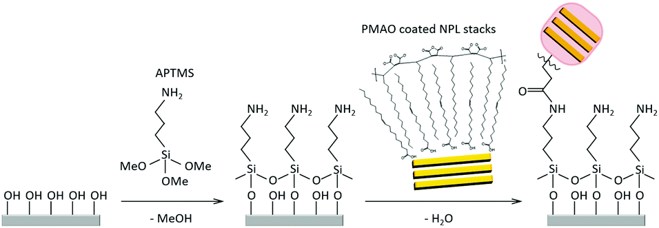 | ||
| Fig. 1 Schematic drawing of the immobilisation process of NPL/polymer hybrid structures onto ITO coated glass electrodes. After a cleaning and hydrophilisation step, the ITO coated glass surfaces are functionalised in a solution consisting of 0.25 v/v% of APTMS in toluene. Subsequently, the electrodes were rinsed carefully with toluene, dried, and then put into diluted solutions of the hybrid structures in KOH. We propose that peptide bonds are formed between the hybrid structures and the APTMS coated ITO glass surface. Notable amounts of hybrid structures were only deposited onto the electrode if KOH was present. | ||
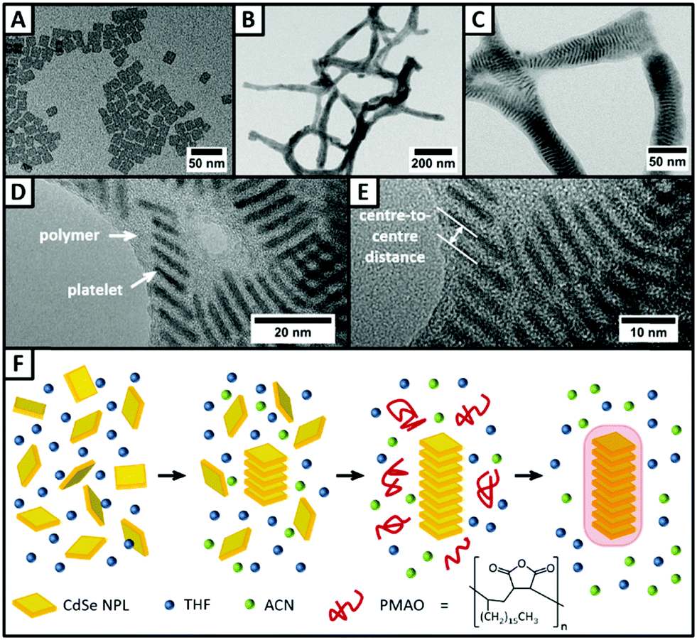 | ||
| Fig. 2 (A) TEM micrograph of the 4 ML thick CdSe NPLs. (B and C) TEM images of NPL–polymer hybrid structures in (B) lower magnification and (C) higher magnification. (D and E) HR-TEM images illustrating the fine structure of the fibres. The CdSe NPLs stand on one of their edges perpendicular to the TEM grid and appear darker. Lattice plains of the NPLs are visible, confirming the crystallinity of the particles. The NPL stacks are surrounded by a polymer shell, which appears in a lighter grey than the NPLs. (F) Schematic representation of the proposed mechanism underlying the hybrid structure formation. | ||
The synthesised NPLs then served as building blocks for the synthesis of NPL–polymer fibres, which could be obtained following a procedure for the synthesis of magnetic nanobeads15 with slight modifications. Quasi-quadratic NPLs with a thickness of 4 MLs were chosen as building blocks, as they were already employed in the synthesis of highly anisotropic NPL superstructures.8,13,30 However, NPLs with other shapes and thicknesses can be applied likewise, and result in similar fibre-like superstructures (Fig. S4, ESI†). Fig. 2B and C shows TEM micrographs of the as-synthesised fibres consisting of 4 ML thick quasi-quadratic NPLs and PMAO in different magnifications. The lower magnification TEM image (Fig. 2B) illustrates the fibre-like structure of the polymer encapsulated NPL stacks. The obtained fibres can reach lengths of up to several micrometres, while their thickness was observed to be lower than 50 nm. The fine structure of the fibres can be seen more in detail in the higher magnification TEM image (Fig. 2C). Inside the polymer shell, the NPLs appear to be well-ordered in stacks, with up to three stacks being parallel to each other. Within the stacks, uniform distances between the single NPLs of about 3.94 nm ± 0.23 nm (centre-to-centre) are observed. Hence, the surfaces of two neighbouring inorganic NPLs are 2.74 nm apart, assuming a platelet thickness of 1.2 nm.4 The calculated value is only slightly higher than the length of a fully stretched oleic acid molecule (2.5 nm),2 indicating that there is a strong interaction between the oleic acid ligands of two NPLs. The measured NPL–NPL distance is, to the best of our knowledge, amongst the lowest distances between stacked oleic acid-coated NPLs reported so far (Table S1, ESI†). In order to investigate the influence of the polymer on the NPL–NPL distance within the stacks, we varied the amount of polymer solution added during the polymer shell growth experiment. TEM micrographs (Fig. 3) reveal the strong dependence of the fibre structure on the polymer amount. If no polymer is added, as a matter of course, no polymer shells are visible (Fig. 3 top). Moreover, the NPL stacks are less ordered with lots of NPLs lying flat on the TEM grid (Fig. 3 white circles). The distances between the stacked platelets can be derived from high resolution TEM images (Fig. 2D and E). Centre-to-centre distances of 4.42 nm ± 0.28 nm were measured. In addition, some more samples with different polymer amounts were synthesised and investigated by TEM (Fig. 3). If low amounts of polymer are employed (lower than 300 μL), no polymer shells are visible in the TEM micrographs. Moreover, the resulting superstructures are not transferable to aqueous media and can be re-dispersed as single particles by addition of THF. The distances between the NPLs in the polymer-free stacks are slightly larger than in the polymer coated superstructures and were determined to be 4.27 nm ± 0.33 nm, 4.28 nm ± 0.30 nm, and 4.42 nm ± 0.28 nm for 150 μL, 50 μL, and 0 μL of the polymer solution, respectively. If 750 μL of polymer solution is added during the experiment, lower NPL–NPL distances of 3.66 nm ± 0.26 nm were observed, while the thickness of the polymer shell around the platelet stacks did not increase distinctly (in comparison to the original procedure, in which 300 μL of polymer solution was used). It needs to be noted that, due to the low TEM contrast differences between the polymer, the platelets, and the background, no precise determination of the polymer shell thickness was possible. The decrease in the NPL–NPL distance due to polymer encapsulation indicates that a second driving force besides the addition of an antisolvent is involved in the formation process of highly-ordered fibres. In a solution consisting of macromolecules and platelet-shaped nanoparticles, attractive forces between the nanoparticles occur, if their distance is small enough and a certain polymer concentration is reached.21–23 If the macromolecules are not able to access the space between the platelets, the platelets are pushed closer together by an entropic force comparable to the osmotic pressure, the so-called depletion attraction.21–23 On this basis, a mechanism for the formation of the NPL/polymer fibres can be proposed (Fig. 2F). It needs to be noted that, similar to our previous observation employing quasi-spherical magnetic nanoparticles and the same polymer as in the present work,15 for the formation of NPL–polymer hybrid structures a transfer of the NPLs from a hexane medium to a tetrahydrofuran (THF) medium is necessary, in order to prevent polymer aggregation and flocculation during polymer encapsulation. During the first step of the fibre synthesis, small stacks of NPLs are formed by the addition of acetonitrile (ACN). ACN is not able to remove oleic acid ligands from the surface of CdSe nanoparticles,31 but leads to a change in the polarity of the solution and consequently to a reduction of the repulsion between the NPL ligands.32 In the second step, a specific amount of the polymer PMAO, dissolved in a mixture of THF and ACN, is added. The applied polymer molecules consist of approximately 80–150 monomer units and are therefore too large, even if they are coiled, to fit into the spaces between the pre-stacked NPLs. However, the aliphatic chains of the polymer are still able to interact with the native ligands of the NPLs. The interaction leads to the formation of a polymer shell around the NPL stacks with the polymeric anhydride groups facing the surrounding solution. Through the addition of water, a certain proportion of the anhydride rings are opened,15 so that the resulting fibres are soluble in aqueous media.
 | ||
| Fig. 3 TEM micrographs of stacked NPLs partially encapsulated into a polymer shell. The amount of polymer solution added during the experiment increases from top to bottom. If less than 300 μL of polymer solution is added, no polymer shell is formed. The white circles indicate the occurrence of unstacked NPLs. | ||
Characterisation of NPL/polymer fibre-coated electrodes
The so-incorporated functional groups do not only lead to water dispersibility of the fibres but also allow further modification, e.g. linkage to amino group functionalised ITO glass. A scheme explaining the electrode preparation process is shown in Fig. 1. The prepared photoelectrodes were afterward characterised by scanning electron microscopy (SEM, Fig. 4A and B) and UV/vis absorption spectroscopy (Fig. S6, ESI†). The SEM micrographs reveal that the fibres are adsorbed at the electrode surface as a whole rather than being destroyed during the deposition process. However, the major part of the surface of the electrode is not occupied and little accumulations of fibres are present.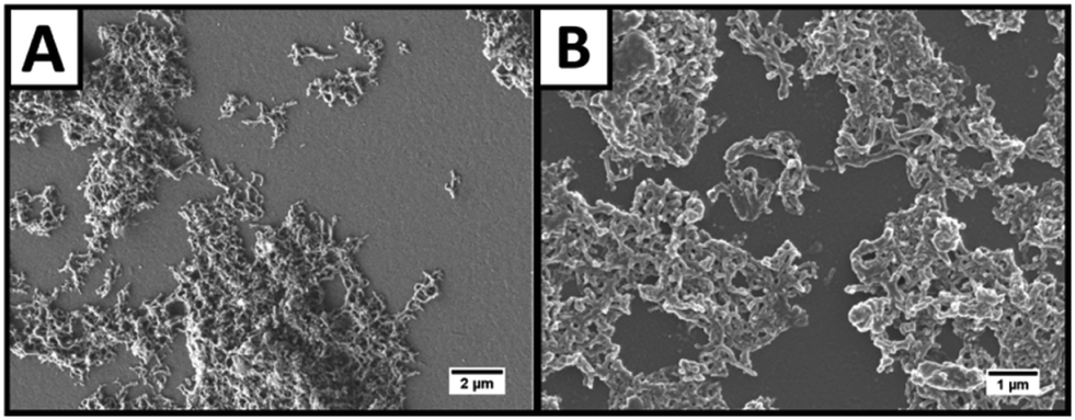 | ||
| Fig. 4 (A and B) SEM micrographs of NPL/polymer hybrid structures at the surface of an APTMS functionalized ITO coated glass electrode in lower (A) and higher (B) magnification. In both images, the elongated shape of the fibres is clearly visible. | ||
It is reasonable to compare the photoelectronic properties of the semiconductor/polymer hybrid material to those of pristine NPLs. All photoelectrochemical measurements were carried out in a self-built measurement cell, which was already applied and described in our previous work.26 Schemes of the applied measurement setup are given in the ESI† (Fig. S11 and S13). For all investigations, a 0.5 M solution of Na2SO3 was used, which acts as a hole scavenger and is therefore able to preserve metal chalcogenides from photocorrosion.33 The chemical photoreactions in this electrolyte system are well understood.24,26 At a bias potential of 150 mV, at which the external photocurrent quantum efficiency (EPQE) spectra were measured, the photooxidation of sulphite ions to sulphate ions takes place. In Fig. 5A and B, the photocurrents of single nanoplatelets as well as the photocurrents of the NPL/polymer hybrid structures are shown in comparison to the UV/vis absorption spectra, which were measured against the pure ITO electrodes. It can be derived that the spectra of the NPL/polymer hybrid structures and the photocurrent spectra of both the hybrid and the single NPLs resemble significantly the UV/vis absorption spectra of the NPLs. If the UV/vis absorption spectra of the single CdSe NPLs and of the fibres are regarded, considerable differences in the peak heights of the two absorption features can be recognised. This phenomenon was reproducibly observed for all samples we investigated. In the work of Antanovich et al.7 a similar phenomenon was shown. They observed an intensity reduction of the absorption peak corresponding to the heavy hole–electron transition as well as a redshift of the absorption bands due to an exchange of the NPL surface ligands, especially if ligands with highly polar headgroups were introduced. However, this effect is in our case only present when the structures are linked to the ITO surface. Hence, the effect of the changing peak heights could originate from an interaction of the semiconductor/polymer hybrid fibres with ITO. The change of the electric environment and the formation of peptide bonds, which could lead to a change of the polymer, are maybe responsible for this effect. As shown in Fig. 5A and B, the EPQE spectra of both systems match well with the UV/vis absorption spectra of the materials, as it is expectable for thin layers of semiconductor nanoparticles.26,34 Only in the case of the hybrid material, a mismatch of the photocurrent and the absorption spectra at wavelengths below 425 nm is recognisable. This difference is caused by the contribution of the semiconductor ITO to the photocurrent, which is at the same order of magnitude in the case of the NPL/polymer hybrid structures, since they have generally lower photocurrent intensities. Note that this contribution of ITO is not observed for the single NPLs, which have a more than one order of magnitude larger photocurrent at comparable optical densities. The platelets inside the fibres are coated by an electrically insulating PMAO shell, which certainly increases the tunnelling barrier between semiconductor, electrolyte, and electrode, and thus lowers the EPQE. Even though tunnelling of electrons from nanoparticles to electrode surfaces across organic molecules with lateral dimensions of 1 to 3 nm has already been shown in the literature,35–37 an explanation for the existence of a tunnelling current in the system could also be an incompletely closed polymer shell. Impedance spectra of the electrodes are supporting this thesis (Fig. S10, ESI†). It is apparent, that the introduction of the polymer into the system increases the occurring resistance of the photoelectrodes. The electrochemical equilibrium of photoreduction and oxidation seems not to be affected in a distinct way by the shell, since the direction of the occurring net photocurrent in linear sweep voltammograms is not changed (Fig. S9, ESI†).26 Under excitation with a 468 nm LED only photocurrent, which is based on platelet illumination, is observable (Fig. 5A and B). To characterise the charge carrier transport across the fibres, IMPS was applied. In this technique, the photon flux of a LED is modulated with a sine wave function, in our case in a frequency range of 10 kHz to 1 Hz by applying an AC voltage to the LED (Fig. S14, ESI†).25 The IMPS complex plane plot of pristine NPLs shows an almost perfect semicircle (Fig. 5C). This semicircle is based on the common concept of photon generated excitons trapped in surface states of the particle.38,39 The excitons can undergo two competing processes, which are the charge transfer of the electron and hole to the electrode and electrolyte, or the recombination of both.24,34 In the case of the fibres, a clear elongation of the IMPS signal can be recognised (Fig. 5D). This is explainable with the superposition of many semicircles, which are attributed to charge transfer between NPLs competing with semiconductor–electrolyte transfer and exciton recombination. Even at a frequency of 1 Hz, the elongated IMPS of the semiconductor/polymer hybrid is not returning to the direction of the real axis. This implies that the system is still not in the steady state in the investigated time domain. The lifetime of trapped charge carriers undergoing NPL–NPL transfer therefore seems to be in the time regime of milliseconds to at least several seconds. Similar results regarding the lifetime of trapped electrons were already obtained for other semiconductor nanoparticle-based devices.40 It has to be mentioned that fluorescence lifetime related studies about exciton transport in NPL stacks carried out by Rowland et al. and Guzelturk et al. are often related to non-trapped excitons undergoing recombination under photoemission.12,13 This distinct category of excitons is characterized by a typically much shorter lifetime, in particular lifetimes between 1.7 and 3.5 ns have been reported for 4 ML thick CdSe NPLs.7,13
 | ||
| Fig. 5 (A and B) Comparison of the wavelength dependent photocurrent efficiency (black) and the UV/vis absorption of pristine 4 ML CdSe NPLs on ITO (A), and of NPL/polymer hybrid structures on ITO (B). The absorption of pure ITO was subtracted from the UV/vis absorption spectra. The photocurrent spectra in both cases are superpositions of the contribution of ITO and that of (A) the NPLs and (B) the NPL/polymer hybrid structures. (C and D) Intensity modulated photocurrent spectra of pristine 4 ML CdSe NPLs on ITO (C), and of NPL/polymer hybrid structures on ITO (D). The spectra were recorded in a frequency range between 10 kHz and 1 Hz. | ||
Conclusions
In summary, we demonstrated the encapsulation of stacked 1D confined NPLs in a polymer, which protects them against dilution-induced dissolution and destruction during phase transfer to aqueous media. Our microscopic investigations clearly reveal the beneficial effect of the chosen polymer for the preservation of an anisotropic structural shape of the obtained highly ordered semiconductor stacks. Moreover, we were able to immobilise the NPL/polymer fibres as a whole on conductive glass electrodes. The polymer shell was observed to support the interconnection between the NPLs but to decrease the electric interplay with the environment. This circumstance is reflected in the different photocurrent kinetics of pristine NPLs and NPL/polymer hybrid structures. The charge carrier kinetics of the fibres, which is not explainable by a single transfer mechanism, reveals a multistep electronic conduction. The conjunction of monodisperse semiconductor nanocrystals into larger arrays is elementary for signal transport and thus a key step in the development of nanoparticle-based photoelectrochemical sensors. Thereby, a connection of large amounts of particles to a limited electrode or chip area on one side, and to an electrolyte as the medium to be analysed on the other side, could be realised. Additionally, the polymer itself could be chemically modified to gain attractive interaction with the analyte or repulsion to impeding substances.Conflicts of interest
There are no conflicts to declare.Acknowledgements
The authors are grateful for financial support from the German Federal Ministry of Education and Research (BMBF) within the framework of the program NanoMatFutur, support code 03X5525, and the European Research Council (European Union's Horizon 2020 research and innovation program, grant agreement 714429). A. S. is thankful for financial support from the Hannover School for Nanotechnology (hsn). Furthermore, the authors would like to acknowledge the Laboratory of Nano and Quantum Engineering (LNQE) at the Leibniz Universität Hannover for support. The authors moreover thank Pascal Rusch for TGA measurements, Vanessa Harms for recording the NMR spectra, and Armin Feldhoff as well as Jürgen Caro for providing the SEM and XRD facilities.References
- S. Ithurria and B. Dubertret, J. Am. Chem. Soc., 2008, 130, 16504–16505 CrossRef CAS PubMed.
- M. D. Tessier, B. Mahler, B. Nadal, H. Heuclin, S. Pedetti and B. Dubertret, Nano Lett., 2013, 13, 3321–3328 CrossRef CAS PubMed.
- A. W. Achtstein, A. Antanovich, A. Prudnikau, R. Scott, U. Woggon and M. Artemyev, J. Phys. Chem. C, 2015, 119, 20156–20161 CrossRef CAS.
- S. Ithurria, M. D. Tessier, B. Mahler, R. P. S. M. Lobo, B. Dubertret and A. L. Efros, Nat. Mater., 2011, 10, 936–941 CrossRef CAS PubMed.
- S. Naskar, J. F. Miethe, S. Sánchez-Paradinas, N. Schmidt, K. Kanthasamy, P. Behrens, H. Pfnür and N. C. Bigall, Chem. Mater., 2016, 28, 2089–2099 CrossRef CAS.
- B. Abécassis, M. D. Tessier, P. Davidson and B. Dubertret, Nano Lett., 2014, 14, 710–715 CrossRef PubMed.
- A. Antanovich, A. Prudnikau, A. Matsukovich, A. Achtstein and M. Artemyev, J. Phys. Chem. C, 2016, 120, 5764–5775 CrossRef CAS.
- M. D. Tessier, L. Biadala, C. Bouet, S. Ithurria, B. Abecassis and B. Dubertret, ACS Nano, 2013, 7, 3332–3340 CrossRef CAS PubMed.
- S. Jana, T. N. T. Phan, C. Bouet, M. D. Tessier, P. Davidson, B. Dubertret and B. Abécassis, Langmuir, 2015, 31, 10532–10539 CrossRef CAS PubMed.
- S. Jana, M. de Frutos, P. Davidson and B. Abécassis, Sci. Adv., 2017, 3, e1701483 CrossRef PubMed.
- E. Beaudoin, B. Abecassis, D. Constantin, J. Degrouard and P. Davidson, Chem. Commun., 2015, 51, 4051–4054 RSC.
- C. E. Rowland, I. Fedin, H. Zhang, S. K. Gray, A. O. Govorov, D. V. Talapin and R. D. Schaller, Nat. Mater., 2015, 14, 484–489 CrossRef CAS PubMed.
- B. Guzelturk, O. Erdem, M. Olutas, Y. Kelestemur and H. V. Demir, ACS Nano, 2014, 8, 12524–12533 CrossRef CAS PubMed.
- M. G. Soliman, B. Pelaz, W. J. Parak and P. Del Pino, Chem. Mater., 2015, 27, 990–997 CrossRef CAS.
- N. C. Bigall, C. Wilhelm, M. L. Beoutis, M. García-Hernandez, A. A. Khan, C. Giannini, A. Sánchez-Ferrer, R. Mezzenga, M. E. Materia, M. A. Garcia, F. Gazeau, A. M. Bittner, L. Manna and T. Pellegrino, Chem. Mater., 2013, 25, 1055–1062 CrossRef CAS.
- Z. Fan, M. K. Serrano, A. Schaper, S. Agarwal and A. Greiner, Adv. Mater., 2015, 27, 3888–3893 CrossRef CAS PubMed.
- L. W. E. Starmans, D. Burdinski, N. P. M. Haex, R. P. M. Moonen, G. J. Strijkers, K. Nicolay and H. Grüll, PLoS One, 2013, 8, 1–9 CrossRef PubMed.
- N. C. Bigall, A. Curcio, M. P. Leal, A. Falqui, D. Palumberi, R. Di Corato, E. Albanesi, R. Cingolani and T. Pellegrino, Adv. Mater., 2011, 23, 5645–5650 CrossRef CAS PubMed.
- S. Wilhelm, T. Hirsch, W. M. Patterson, E. Scheucher, T. Mayr and O. S. Wolfbeis, Theranostics, 2013, 3, 239–248 CrossRef CAS PubMed.
- T. Pellegrino, L. Manna, S. Kudera, T. Liedl, D. Koktysh, A. L. Rogach, S. Keller, J. Rädler, G. Natile and W. J. Parak, Nano Lett., 2004, 4, 703–707 CrossRef CAS.
- S. Asakura and F. Oosawa, J. Chem. Phys., 1954, 22, 1255–1256 CrossRef CAS.
- S. Asakura and F. Oosawa, J. Polym. Sci., 1958, 33, 183–192 CrossRef CAS.
- T. G. Mason, Phys. Rev. E: Stat., Nonlinear, Soft Matter Phys., 2002, 66, 060402 CrossRef CAS PubMed.
- S. G. Hickey and D. J. Riley, Electrochim. Acta, 2000, 45, 3277–3282 CrossRef CAS.
- L. Dloczik, O. Ileperuma, I. Lauermann, L. Peter, E. A. Ponomarev, E. A. Ponomarev, G. Redmond, N. J. Shaw and I. Uhlendorf, J. Phys. Chem. B, 1997, 101, 10281–10289 Search PubMed.
- J. F. Miethe, F. Lübkemann, J. Poppe, F. Steinbach, D. Dorfs and N. C. Bigall, ChemElectroChem, 2018, 5, 175–186 CrossRef CAS.
- E. a. Ponomarev and L. M. Peter, J. Electroanal. Chem., 1995, 396, 219–226 CrossRef.
- M. D. Tessier, P. Spinicelli, D. Dupont, G. Patriarche, S. Ithurria and B. Dubertret, Nano Lett., 2014, 14, 207–213 CrossRef CAS PubMed.
- B. Abécassis, M. D. Tessier, P. Davidson and B. Dubertret, Nano Lett., 2014, 14, 710–715 CrossRef PubMed.
- B. Abécassis, M. D. Tessier, P. Davidson and B. Dubertret, Nano Lett., 2014, 14, 710–715 CrossRef PubMed.
- A. Hassinen, I. Moreels, K. De Nolf, P. F. Smet, J. C. Martins and Z. Hens, J. Am. Chem. Soc., 2012, 134, 20705–20712 CrossRef CAS PubMed.
- B. Abécassis, ChemPhysChem, 2016, 17, 618–631 CrossRef PubMed.
- M. J. Berr, A. Vaneski, C. Mauser, S. Fischbach, A. S. Susha, A. L. Rogach, F. Jäckel and J. Feldmann, Small, 2012, 8, 291–297 CrossRef CAS PubMed.
- S. G. Hickey, D. J. Riley and E. J. Tull, J. Phys. Chem. B, 2000, 104, 7623–7626 CrossRef CAS.
- R. Koole, P. Liljeroth, C. De Mello Donegá, D. Vanmaekelbergh and A. Meijerink, J. Am. Chem. Soc., 2006, 128, 10436–10441 CrossRef CAS PubMed.
- F. P. Zamborini, M. C. Leopold, J. F. Hicks, P. J. Kulesza, M. A. Malik and R. W. Murray, J. Am. Chem. Soc., 2002, 124, 8958–8964 CrossRef CAS PubMed.
- I. Willner, F. Patolsky and J. Wasserman, Angew. Chem., Int. Ed., 2001, 40, 1861–1864 Search PubMed.
- D. Klotz, D. S. Ellis, H. Dotan and A. Rothschild, Phys. Chem. Chem. Phys., 2016, 18, 23438–23457 RSC.
- J. Li and L. M. Peter, J. Electroanal. Chem., 1985, 193, 27–47 CrossRef CAS.
- A. Pockett, G. E. Eperon, N. Sakai, H. J. Snaith, L. M. Peter and P. J. Cameron, Phys. Chem. Chem. Phys., 2017, 19, 5959–5970 RSC.
Footnotes |
| † Electronic supplementary information (ESI) available. See DOI: 10.1039/c8tc03879a |
| ‡ These authors contributed equally. |
| This journal is © The Royal Society of Chemistry 2018 |