Colloidal tin sulfide nanosheets: formation mechanism, ligand-mediated shape tuning and photo-detection†
Received
25th May 2018
, Accepted 7th August 2018
First published on 9th August 2018
Abstract
Colloidal materials of tin(II) sulfide (SnS), as a layered semiconductor with a narrow band gap, are emerging as a potential alternative to the more toxic metal chalcogenides (PbS, PbSe, CdS, and CdSe) for various applications such as electronic and optoelectronic devices. We describe a new and simple pathway to produce colloidal SnS nanosheets with large lateral sizes and controllable thicknesses, as well as single-crystallinity. The synthesis of the nanosheets is achieved by employing tin(II) acetate as the tin precursor instead of harmful precursors such as bis[bis(trimethylsilyl)amino] tin(II) and halogen-involved precursors like tin chloride, which limits their large-scale production. We successfully tuned the morphology between squared nanosheets with lateral dimensions from 150 to about 500 nm and thicknesses from 24 to 29 nm, and hexagonal nanosheets with lateral sizes from 230 to 1680 nm and heights ranging from 16 to 50 nm by varying the ligands oleic acid and trioctylphosphine. The formation mechanism of both shapes has been investigated in depth, which is also supported by DFT simulations. The optoelectronic measurements show their relatively high conductivity with a pronounced sensitivity to light, which is promising in terms of photo-switching, photo-sensing, and photovoltaic applications and also due to their reduced toxicity.
Introduction
Two-dimensional (2D) metal chalcogenides serve as building blocks in various applications, including catalysis, batteries, solar cells, optoelectronics, and thermoelectric energy harvesting, owing to their unique size- and shape-dependent optical and electrical properties compared to 0D nanoparticles and also 1D nanorods.1–8 2D nanomaterials comprising lead or cadmium chalcogenides such as PbS, PbSe, CdS and CdSe have been intensively investigated. They exhibit tunable optoelectronic properties, which are often superior to their bulk counterparts.9–12 However, they also display high toxicity, which hampers their applicability. To mitigate this problem, further studies of more environmentally friendly and less toxic semiconductors are necessary. One promising class of materials are tin chalcogenides.13–15 In particular, tin(II) sulfide (SnS), a p-type semiconductor with an indirect bulk band gap of 1.07 eV and a direct band gap of 1.3 eV, shows both a high absorption coefficient and a good hole mobility.16,17 Typically, SnS adopts a layered orthorhombic (OR) crystal structure (space group: Pbnm). SnS can be described as a highly distorted rock salt structure with atomic double layers, which are covalently bonded in the plane and van der Waals bonded in the vertical b direction (a = 4.33 Å, b = 11.19 Å, and c = 3.98 Å). The latter is due to a chemically inert surface without any dangling bonds, which leads to its relatively high chemical stability and shows 2D morphology.18,19 Recently, theoretical and experimental studies showed the extraordinary properties of 2D SnS such as selected valleys’ optical excitation, ferroelectric and piezoelectric properties, which further motivate the development of cheap and safe methods for 2D morphology.20,21
Recently, several studies focused on the synthesis of 2D SnS nanostructures. However, most of the materials are produced by demanding physical methods such as physical vapor deposition, molecular beam epitaxy and mechanical exfoliation, which usually yield polydisperse, irregular-shaped SnS nanosheets (NSs).22–24 Compared to physical methods, colloidal syntheses can produce NSs from solution, assisted by surfactants to control their growth with uniform lateral dimensions, regular faceted edges and tunability. Such nanostructures can be processed by simple means, such as spin coating and drop casting,25 which is a prerequisite for efficient and inexpensive manufacture of super-assembled structures or deposition on flexible substrates for further applications.26 However, most of the published synthesis procedures for SnS (analogically SnSe) yield mainly nanocubes and nanoparticles.16,27,28 A few synthesis procedures of colloidal 2D SnS nanosheets have been reported so far, but most of them are synthesized with halogen involved tin precursors (e.g. tin(IV) tetrachloride pentahydrate, tin(II) chloride) or with the assistance of hexamethyldisilazane (HMDS) for 2D nanomaterial formation.16,29–31
For the colloidal synthesis of 2D SnS NSs in the present work, tin(II) acetate was used as the tin precursor, which can be partly converted into the corresponding Sn–oleate complex during the conditioning step in the presence of oleic acid and can partly serve as the ligand for NS formation. In this process, no halogen ions are involved (e.g. through tin(II) chloride or tin(IV) chloride). Halogen ions in the synthesis of SnS NSs have been reported to be fully complexed by HMDS and be completely removed to avoid the inhibition of the formation of SnS NSs.31,32 Thus, the introduction of chloride ions is not necessary. The precursor bis[bis(trimethylsilyl)amino] tin(II) has been reported to yield rectangular NSs with a size of 7 μm × 20 nm.33 However, this type of tin precursor is very flammable with low stability and high reactivity. Here, we introduce a halogen- and HMDS-free synthesis of NSs, involving no flammable precursor as well. This shows that oleic acid (OA) and trioctylphosphine (TOP) amounts have strong control over shape and size (150–1680 nm). Based on experimental data and DFT calculations, we rationalize the shape changes in SnS NSs and propose an approach where the shape can be tuned between squared and hexagonal. The samples’ crystal phase can be obtained as single-crystalline OR without other phases being involved (e.g. pseudotetragonal phase from byproducts). We investigated the detailed mechanism of ligand–facet interactions to form NSs with different sizes and shapes, as well as the function of the precursors. Eventually, by contacting individual NSs, their performance in terms of conductivity and photoconductivity has been investigated, revealing their outstanding optoelectronic properties.
Experimental section
Materials
Tin(II) acetate (TA, 100%), oleic acid (OA, technical grade, 90%), trioctylphosphine (TOP, 97%), diphenyl ether (DPE, Reagent plus, ≥99%), toluene, and dimethylformamide (DMF) were purchased from Sigma-Aldrich and were all used as-received without additional purification. Thioacetamide (TAA, ACS Reagent Grade, 99%) was bought from Fisher Scientific (Acros Organics). Thioacetamide, trioctylphosphine and tin(II) acetate were all stored in a glovebox.
Synthesis of square-like 2D SnS nanosheets
In a typical synthesis procedure, a round-bottom three-necked 50 mL flask fitted with a condenser, a septum and a thermocouple was used. 59.2 mg (0.25 mmol) of TA, 0.2 mL (0.64 mmol) of OA and 0.5 mL of TOP (1.0 mmol) were dissolved in 10 mL of DPE. The mixture was degassed and dried under vacuum for 2 h at 75 °C, partially transforming tin acetate into tin oleate and removing the free acetic acid from the system as well. After the vacuum step, the mixture was heated to 230 °C under the nitrogen flow. After temperature stabilization (15 min), 19.5 mg (0.26 mmol) of TAA in 0.2 mL of DMF was injected rapidly into the reaction solution. After 5 min, the heating mantle was removed and the resulting solution was allowed to cool to room temperature. The resultant nanostructures were then purified by centrifugation with toluene at 4000 rpm for 3 min (2–3 times). The product could then be re-suspended in toluene for further characterization or storage. To investigate the influence of different parameters, the other reaction parameters are kept constant.
Characterization
Transmission electron microscopy (TEM) images and selected area electron diffraction (SAED) patterns were obtained using a JEOL-1011 operated at 100 kV. All the TEM samples were prepared by dropping 10 μL of diluted toluene dispersion onto carbon-coated TEM grids followed by solvent evaporation under ambient conditions. The high-resolution (HR) TEM images were obtained using a Philips CM300 UT microscope operated at 200 kV. The X-ray diffraction (XRD) patterns were obtained using a Philips X’Pert System in Bragg–Brentano geometry, together with a copper anode at an X-ray wavelength of 0.154 nm. The samples were prepared by drop casting of a well-suspended NS solution on silicon substrates. The surface topology data were obtained using an atomic force microscope (AFM) from JPK Instruments in intermittent contact mode. The samples were prepared by drop-casting a diluted NS suspension on a silicon chip. The samples were also measured by scanning electron microscopy (SEM) using a LEO GEMINI 1550 microscope for morphological information.
Device preparation
SnS NSs suspended in toluene were spin-coated on silicon wafers with a 300 nm thermal silicon oxide layer as the gate dielectric. The highly doped silicon was used as the back gate. The individual NSs were contacted by e-beam lithography followed by thermal evaporation of Ti/Au (1/55 nm) and the lift-off process.
Device measurements
Immediately after device fabrication, the samples were transferred to a probe station (Lakeshore Desert) connected to a semiconductor parameter analyzer (Agilent B1500a). All the measurements have been performed in a vacuum at room temperature. The vacuum chamber has a view port above the sample which is used for sample illumination. For illumination of the NSs, a red laser (627 nm, 1–16 mW) with a spot size of 2 mm was used.
DFT simulations
In order to evaluate the adsorption energies of the ligands on different crystal facets, simulations based on density functional theory (DFT) were employed. For that, the crystal geometry had been kept fixed to the experimental values for OR–SnS and the ligands were free to relax by geometry optimization. We used the versatile software package CP2K with the PADE LDA functional, the DZVP basis set, and a corresponding GTH-PADE potential. An individual SnS nanocrystal with 224 Sn and 224 S atoms and the respective ligand molecules are simulated under periodic boundary conditions where the box dimensions are sufficiently large to avoid their interactions between neighboring virtual molecular structures.
Results and discussion
In the following we discuss the influence of various parameters on the synthesis of SnS nanosheets. This allows drawing conclusions on the formation mechanism and their crystallography. Eventually, we demonstrate their optoelectronic responses.
Synthesis of colloidal square-like SnS nanosheets
TA, OA and TOP in DPE were degassed at 75 °C and then heated to a reaction temperature of 230 °C under a nitrogen flow, followed by the hot injection of TAA, as sulfide precursor, to obtain fast nucleation and growth of 2D NSs. To guarantee the repeatability of the procedure, we kept the injection volume constant (0.2 mL) for all experiments. During preheating and degassing phases, TA as the tin precursor was partly transformed to tin oleate in the presence of OA. When tin(II) chloride was used as the precursor, only irregularly shaped NSs and byproducts were formed with an otherwise unchanged procedure (Fig. S1, ESI†). A TEM image of square-like SnS NSs with a lateral size of approximately 460 nm is shown in Fig. 1a. SAED (Fig. 1b) patterns reveal their single-crystallinity due to the well-ordered dot pattern, which matches the list of reflections of OR–SnS bulk (the International Centre for Diffraction Data (ICDD) card 00-039-0354), respectively showing the diffraction planes (200), (101), and (002). The X-ray diffractogram (Fig. 1c) of the capillary powder sample is also consistent with the crystallography for OR–SnS bulk. For the drop-casted SnS NS films, two pronounced peaks (040) and (080) are observed, representing the highly textured [010] orientation, which corresponds to the thickness. The Scherrer analysis of the (040) peak in the film sample reveals a thickness of 29 nm for the sample shown in Fig. 1c. A SEM image (Fig. 1d) gives an overview on the morphology of the NSs, which shows the squared NSs with smooth surfaces and some squared NSs with truncated edges. An AFM image of the square-like SnS NSs is shown in Fig. S2 (ESI†) and the measured thickness is 31 nm.
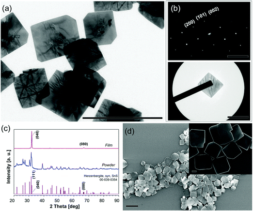 |
| | Fig. 1 (a) TEM image of square-like SnS NSs synthesized using the standard synthesis process. Scale bar = 1 μm. (b) SAED pattern of a single nanosheet and its corresponding TEM image. (c) XRD patterns of SnS NSs drop-casted on a Si wafer (thin film) and a powder sample in a capillary tube. (d) SEM images of SnS NSs (scale bar = 1 μm, inset: larger magnification: scale bar = 100 nm). | |
Influence of trioctylphosphine on the synthesis of square-like single-crystal SnS nanosheets
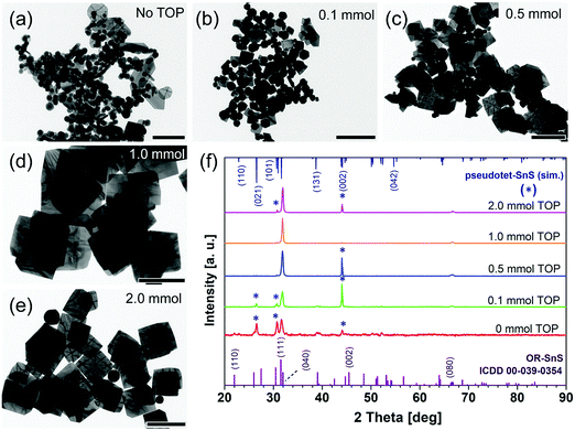
The synthesis of SnS NSs proceeds in two steps. First, the complexation of the tin precursor in the presence of OA happens before the injection of the second precursor. Second, the reaction between the tin and sulfur precursors takes place to form nuclei, which is followed by the growth process to produce SnS NSs. Theoretically, the crystal facets with a lower surface energy have a slower growth speed in order to minimize the total surface energy of the whole crystal based on the Gibbs–Curie–Wulff theorem and the Wulff construction.34,35 Furthermore, the reason for the anisotropic growth of 2D nanocrystals is mainly due to the different surface energies of the facets according to the selective adsorption of ligands. Thus, different growth speeds on each facet capped with certain ligands lead to the final shape of the nanostructures. When there is no TOP and no OA in the synthesis, SnS nanoparticles and squared nanoplatelets (≤100 nm) are obtained (Fig. S3, ESI†). This indicates that the acetate can facilitate the formation of 2D nanostructures without TOP or OA in the synthesis, which is also supported by DFT simulations on the adsorption energy in Table 1. They show that acetate (AA−) as the ligand binds strongly to the (100) and (101) side facets, and also binds strongly to the (010) facets, which could lead to truncated rectangular small nanoplatelets. However, it is shown that only acetate can mostly produce nanoparticles. When no TOP was involved in the synthesis, spherical nanoparticles and hexagonal NSs (Fig. 2a and Fig. S3b, ESI†) were synthesized with a constant amount of OA (0.64 mmol) and all other parameters remain unchanged. This is due to the strong bond of oleate on the (100) and (101) (or {101}) facets, which facilitate the hexagonal shape (elongated facet is (100), Fig. S3b, ESI†). A TEM image of the synthesis with 0.1 mmol TOP (Fig. 2b) shows that most of the products were nanoparticles, accompanied by small hexagonal-shaped and square-shaped nanoplatelets. The appearance of square-shaped nanocrystals is consistent with the simulation data for TOP, revealing that adsorption energies on the {101} facets are larger than others. By comparing the product with only OA ligands as shown in Fig. 2a, it is indicated that this small amount of TOP still exerts its influence to maintain the 2D square-shaped nanostructure formation (∼160 nm). More squared sheets with increased edge lengths of 240 nm were produced together with less irregular nanoparticles when 0.5 mmol of TOP was used (Fig. 2c). 1.0 mmol TOP led to larger (nearly 460 nm) squared sheets without byproducts. Further, doubling the amount of TOP made no significant difference. Therefore, TOP plays an important role in retaining the growth of square-shaped NSs with the acetate ligands, while OA facilitates the formation of hexagonal shaped nanostructures.
Table 1 Adsorption energies [eV] of ligand molecules on the (100), (101), (010) facets of SnS calculated by the density functional theory (DFT) method. The simulations were performed using the full version of acetate (AA−) and simplified molecules for TOP, OA and oleate (triethylphosphine (TEP) and tributylphosphine (TBP) for TOP, butyric acid (BA) for OA, and BA− (butyrate) for the oleate). The simplified TOP, OA and oleate molecules were used to enable reasonable calculation times and to avoid additional contributions by the adsorption of the side chains. Anyhow, simulations on different chain lengths (C2 and C4) show that the tendencies are similar
|
|
SnS-101 side facet (isotropic) |
SnS-100 side facet (anisotropic-zigzag) |
SnS-010 top facet (Top or down) |
| TEP (C2) |
1.834 |
1.842 |
0.651 |
| TBP (C4) |
2.061 |
2.060 |
0.772 |
| AA− (C2) |
3.661 |
4.453 |
2.506 |
| AA (C2) |
0.988 |
1.358 |
0.551 |
| BA− (C4) |
3.635 |
4.355 |
2.547 |
| BA (C4) |
1.076 |
1.120 |
0.623 |
 |
| | Fig. 2 (a–e) TEM images of 2D SnS nanostructures with different TOP amounts (0–2.0 mmol). Scale bar is 200 nm for (a) and 500 nm for (b–e). (f) Powder XRD patterns of SnS NSs. | |
The XRD data (Fig. 2f) show a more and more prominent (040) peak compared to other suppressed peaks with increasing amounts of TOP, which indicates that more squared and larger 2D nanostructures as well as less byproducts (such as nanoparticles or nanoplatelets) were produced. The intensity of the diffraction peak at 44.04° is reduced when the amount of TOP increases from 0.0 mmol to 2.0 mmol TOP. This diffraction peak does not match the standard diffraction pattern of OR–SnS bulk, but this peak is close to (220) of the zinc blend (ZB) phase (43.8°). Theoretically, ZB SnS is a metastable phase, which is only kinetically stable and protected by a certain specific energy barrier avoiding its transformation to OR–SnS.36,37 However, it can be better explained by convolutions of 43.9° and 44.1° of the pseudotetragonal (PT) structure, as it is a more stable crystal phase under given conditions.16 The XRD measurement for the powder sample in a capillary tube (Fig. S4, ESI†) more clearly demonstrates that the samples using 0.1 mmol of TOP show a mixture of OR and PT crystal structures, together with several small peaks (2Θ = 32.7° and 35.5°) stemming from the planes (12![[1 with combining macron]](https://www.rsc.org/images/entities/char_0031_0304.gif) ) and (031) of crystalline sulfur (ICDD card 01-072-2402). In addition, the peaks at 30.7° and 26.5° also stand for (101) and (021) of the PT structure. The SAED patterns also reveals that the nanosheets are of OR-type and the PT phase belongs to the byproduct (nanoparticle, Fig. S5a and b, ESI†). An increasing yield of crystalline SnS NSs could be obtained when we used TOP in amounts of up to 1.0 mmol in our case, with the gradual disappearance of PT particle products.
) and (031) of crystalline sulfur (ICDD card 01-072-2402). In addition, the peaks at 30.7° and 26.5° also stand for (101) and (021) of the PT structure. The SAED patterns also reveals that the nanosheets are of OR-type and the PT phase belongs to the byproduct (nanoparticle, Fig. S5a and b, ESI†). An increasing yield of crystalline SnS NSs could be obtained when we used TOP in amounts of up to 1.0 mmol in our case, with the gradual disappearance of PT particle products.
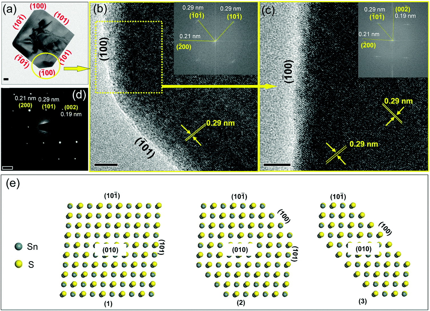
The thickness values calculated from the XRD data are in the range of 24 to 29 nm with increasing amounts of TOP (AFM shown in Fig. S6, ESI†). The SAED patterns of a single-truncated square sheet from the synthesized sample with 1.0 mmol TOP (Fig. 3) with two non-truncated diagonal corners and other two truncated corners are investigated. The HRTEM images (Fig. 3b, c and Fig. S7, ESI†) and the corresponding FFTs (inset) revealing the four planes corresponding to the four sides of the square-shaped sheet are the {101} planes. This is also confirmed by the electron diffraction patterns in Fig. 3d. The SAED patterns reveal the facets of (200), (002) and (101) which are also identified in the corresponding TEM images in Fig. 3a (SAED patterns are rotated with respect to the TEM image by instrumentation). The truncated facets are found to be the (100) and (00) facets. Fig. 3e shows models for SnS NSs with square shape (Fig. 3e(1)), truncated square shape (Fig. 3e(2)) and highly truncated or hexagonal shape (Fig. 3e(3)). The atomic arrangements of the (101) and (01) facets (Fig. 4a and b) show that the Sn and S atoms are alternatively ordered. In principle, each S (or Sn) atom in these facets has three bonds, from which one bond always forms a bond with S (or Sn) perpendicular to the facets. As L-type ligands, TOP prefers to bind to metal centers. Our DFT simulations (Table 1) show the interaction between TOP and Sn atoms on the (101) facet and also demonstrate that TOP binds to the {101} facets most strongly and it displays a weak preference for the (010) facet. Therefore, acetate ligands lead to squared 2D SnS nanoplatelets and TOP can help to maintain the square shape and enlarge the size of the nanoplatelets to large nanosheets.
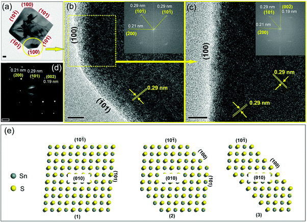 |
| | Fig. 3 (a) TEM image of a single SnS NS obtained using the standard synthesis method with two non-truncated diagonal corners and other two truncated corners. The HRTEM image reveals a lattice spacing of 0.29 nm (b and c), which is consistent with the spacing of {101} planes. The SAED patterns (d) show the lattice fringes of the (200), (002) and (101) crystal facets. The corresponding facets of (00) and (01) are recognized based on the FFT analysis in insets of (b and c), confirming the faceting in (a). A set of atomic models of SnS NSs with shapes changing from squared to hexagonal (e). All these three models drawn here contained two layered atoms and that was the reason why certain overlapping could be seen from the figure (grey Sn atoms overlap yellow S atoms, or yellow S atoms overlap grey Sn atoms). The scale bar is 50 nm in (a), 5 nm in (b and c), and 5 μm in (d). | |
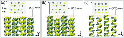 |
| | Fig. 4 (a–c) The atomic arrangements in the (101), (01) and (100) planes of SnS nanocrystals respectively. The top views of each model are also shown to demonstrate the exposed atoms on these three facets. | |
Influence of the oleic acid amount on the synthesis of square-like single-crystal SnS nanosheets
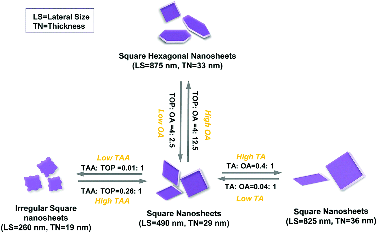
When only TOP and no OA is introduced in the synthesis, small squared sheets and nanoparticles both appear in the product (Fig. 5a and Fig. S8a, ESI†). This matches the simulation data for TOP, indicating that TOP can enhance the formation of (101)-facet square NSs (Fig. S8a, ESI†). Further, we investigated the influence of the OA amount on the morphology of synthesized SnS NSs, keeping TOP (1.0 mmol) and other parameters constant. The TEM images of the synthesis using 0.32–0.64 mmol of OA in Fig. 5a–c show a lateral size change from 180 nm to 380 nm and thickness increase from 16 nm to 29 nm (derived from XRD, no shape change, and still square-like sheets), together with a higher degree of uniformity in lateral size. Moreover, squared NSs as well as nanoparticles were observed with a low amount of OA (OA ≤ 0.64 mmol and TA![[thin space (1/6-em)]](https://www.rsc.org/images/entities/char_2009.gif) :OA ratio ≤ 1:2.5). This is due to the fact that the strong adsorption energy of TOP on (101) dominates (Table 1), which assist the formation of squared sheets with the original acetate in the synthesis. The simulations are performed using simplified molecules for OA and oleate (represented by butyric acid as BA and butyrate as BA−). The hexagonal shape starts to appear when the OA amount is larger than 2 mmol, which we consider as the minimum amount of OA for the formation of hexagonally shaped sheets. Lateral size and thickness values both increase highly (33 nm to 53 nm) when 12 times more OA than TA is applied (OA ≥ 3.2 mmol and TA:OA ratio ≥ 1:12). Based on the law of mass action, the higher the amount of OA, the higher the possibility for OA to bind to the surface of the crystals, substituting the oleate. OA (L-type ligand) is a weaker ligand than oleate (X-type ligand), which facilitates the monomers to react on the crystal surface compared to the case of oleate as the ligand, helping to grow larger and thicker sheets under otherwise unchanged conditions. Higher OA amounts (≥3.2 mmol) trigger the shape change from square-like to hexagonal nanostructures and strongly influence the size (TA:OA ratio ≥ 1:12, especially 1:25). Analysis of the lateral sizes calculated from TEM images (Fig. 5) shows a dramatic increase (from 160 nm to 1600 nm, OA was used from 0.32 mmol to 6.4 mmol). This confirms that OA plays a major role in the size and shape tuning from squared to hexagonal SnS NSs. This is due to the largest adsorption energy of neutral OA ligands (represented by butyric acid as BA, Table 1) on (100) facets compared to those on (101) or (010) facets, facilitating the formation of hexagonal NSs with elongated edges when there is an excess of OA ligands (≥3.2 mmol) (Fig. S8b, ESI,† with 6.4 mmol OA). The XRD measurements show a further pronounced (040) peak for higher OA amounts, indicating that a suitable quantity of OA could lead to stable OR–SnS nanostructures. The size and shape evolution of SnS NSs are sketched in Fig. 6, and this shows how OA with TOP influences the formation of SnS NSs.
:OA ratio ≤ 1:2.5). This is due to the fact that the strong adsorption energy of TOP on (101) dominates (Table 1), which assist the formation of squared sheets with the original acetate in the synthesis. The simulations are performed using simplified molecules for OA and oleate (represented by butyric acid as BA and butyrate as BA−). The hexagonal shape starts to appear when the OA amount is larger than 2 mmol, which we consider as the minimum amount of OA for the formation of hexagonally shaped sheets. Lateral size and thickness values both increase highly (33 nm to 53 nm) when 12 times more OA than TA is applied (OA ≥ 3.2 mmol and TA:OA ratio ≥ 1:12). Based on the law of mass action, the higher the amount of OA, the higher the possibility for OA to bind to the surface of the crystals, substituting the oleate. OA (L-type ligand) is a weaker ligand than oleate (X-type ligand), which facilitates the monomers to react on the crystal surface compared to the case of oleate as the ligand, helping to grow larger and thicker sheets under otherwise unchanged conditions. Higher OA amounts (≥3.2 mmol) trigger the shape change from square-like to hexagonal nanostructures and strongly influence the size (TA:OA ratio ≥ 1:12, especially 1:25). Analysis of the lateral sizes calculated from TEM images (Fig. 5) shows a dramatic increase (from 160 nm to 1600 nm, OA was used from 0.32 mmol to 6.4 mmol). This confirms that OA plays a major role in the size and shape tuning from squared to hexagonal SnS NSs. This is due to the largest adsorption energy of neutral OA ligands (represented by butyric acid as BA, Table 1) on (100) facets compared to those on (101) or (010) facets, facilitating the formation of hexagonal NSs with elongated edges when there is an excess of OA ligands (≥3.2 mmol) (Fig. S8b, ESI,† with 6.4 mmol OA). The XRD measurements show a further pronounced (040) peak for higher OA amounts, indicating that a suitable quantity of OA could lead to stable OR–SnS nanostructures. The size and shape evolution of SnS NSs are sketched in Fig. 6, and this shows how OA with TOP influences the formation of SnS NSs.
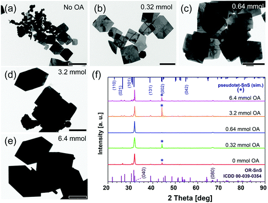 |
| | Fig. 5 (a–e) The shape and size change of SnS nanoparticles to nanosheets synthesized using various OA amounts (0–6.4 mmol). Scale bars correspond to 500 nm, 200 nm, 500 nm, 1 μm, and 1 μm respectively from (a) to (e). (f) Powder XRD patterns of SnS NSs from (a) to (e). | |
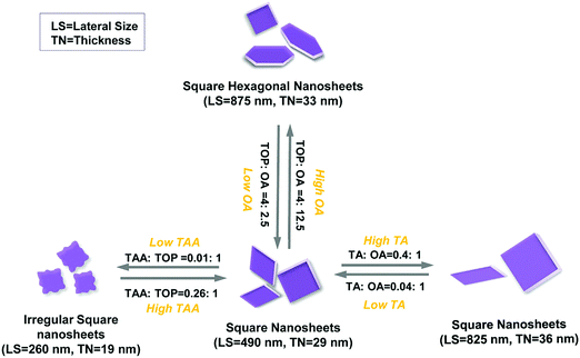 |
| | Fig. 6 The schematic illustration of the formation and shape evolution of SnS nanostructures. LS = lateral size and TN = thickness. | |
Effect of the precursor amount
The amounts of precursors will define the numbers of nuclei for further growth. We found that with an increase in the amount of tin precursor, there is a dramatic drop in size (Fig. 7). When 0.025 mmol of TA is used, the lateral size reaches 826 nm, along with a thickness of 36 nm (Fig. 7). In the cases of lower TA amounts (<0.25 mmol), larger and thicker sheets are formed after the injection of the sulfide source. The lesser the amount of tin source, the lower the number of nuclei that can form, which then causes the formation of larger and thicker NSs. When the amount reaches 0.5 mmol TA, the nanoparticles appear due to excess amounts of acetate ligands. Different amounts of sulfur source are also investigated to elucidate the influence on the SnS NS synthesis (Fig. S9, ESI†). Considering the amount of sulfur precursor, the TEM images reveal that lower amounts (≤0.13 mmol) only lead to irregular shaped NSs. But these irregular sheets are still highly crystalline with OR crystal structures (Fig. S10, ESI†). This is attributed to the lack of sulfur monomers for further growth of NSs. The XRD measurements also demonstrate that with an increase in the amount of sulfur precursor, the (040) and (080) peaks are more pronounced and other peaks are more suppressed (Fig. S9, ESI†). When the amount of TAA reaches 0.26 mmol, lateral size and thickness begin to level off.
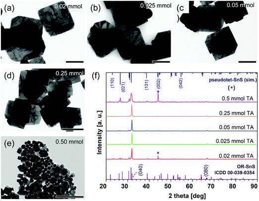 |
| | Fig. 7 (a–e) The shape and size change of 2D SnS nanoparticles to nanosheets synthesized using an amount of tin acetate from 0.02 mmol to 0.025, 0.05, 0.25, and 0.5 mmol. All scale bars correspond to 500 nm. (f) Powder XRD patterns of SnS NSs from (a) to (e). | |
Therefore, we propose a growth mechanism for the formation of 2D SnS nanosheets based on our approach. Firstly, tin ions are coordinated by acetate (Sn-acetate), as tridentate bridging ligands with certain chelating character, forming a strongly distorted trigonal bipyramid for the first coordination sphere.38 TAA thermally decomposes by hot injection, producing S2− for further reaction with Sn2+ ions. Therefore, SnS nuclei are formed after TAA decomposition, passivated by the ligands on the surface of nuclei. With the injection of the sulfur source, the acetate ligands trigger the formation of SnS nanoparticles and squared nanoplatelets (≤100 nm) without OA and TOP in the reaction due to the dominated passivation on the {101}, (100) and (010) facets by acetate. When OA was introduced in the synthesis (0.64 mmol), hexagonal sheets and small nanoparticle byproducts are obtained, whereas square sheets are prepared with TOP involved (1.0 mmol) in the synthesis without OA, because of strong bonds of oleate ligands on (100) and {101}. When OA is applied and the amount of OA is lower than 3.2 mmol together with 1.0 mmol TOP, Sn-acetate is partly replaced with Sn-oleate during the vacuum step, leading to the formation of still squared SnS NSs (∼460 nm) without byproducts. However, hexagonal NSs are formed when the OA amount is higher with a constant TOP amount. Thus, the shape of the NSs is due to the balance between TOP and OA, as well as the original acetate ligands. For that, tuning the amounts of TOP and OA can tune the shape between squared and hexagonal NSs. When the appropriate ratio of TOP/OA is used in the synthesis, the product can be obtained as pure OR–SnS nanosheets without PT-type byproducts.
Electrical measurements
In order to investigate the potential application of the nanosheets, we measured the conductivity and photoconductivity of individually contacted SnS NSs. Fig. 8a shows the I–V characteristics of the NSs in the dark and under different illumination powers. The dark conductivity of the NSs is relatively higher than comparable materials such as colloidal PbS nanosheets (7.9 S m−1, which is up to one order of magnitude higher than the conductivity of PbS nanosheets).39 Upon illumination of the sheets with a red laser (λ = 627 nm), the current increases, which is attributed to an increased carrier concentration due to the optical excitation and generation of electron–hole pairs. The sensitivity of the device, defined by (Iill − Idark)/Idark, reaches 0.95. Further, we calculated the spectral response Rλ and detectivity D* by employing the following equations.
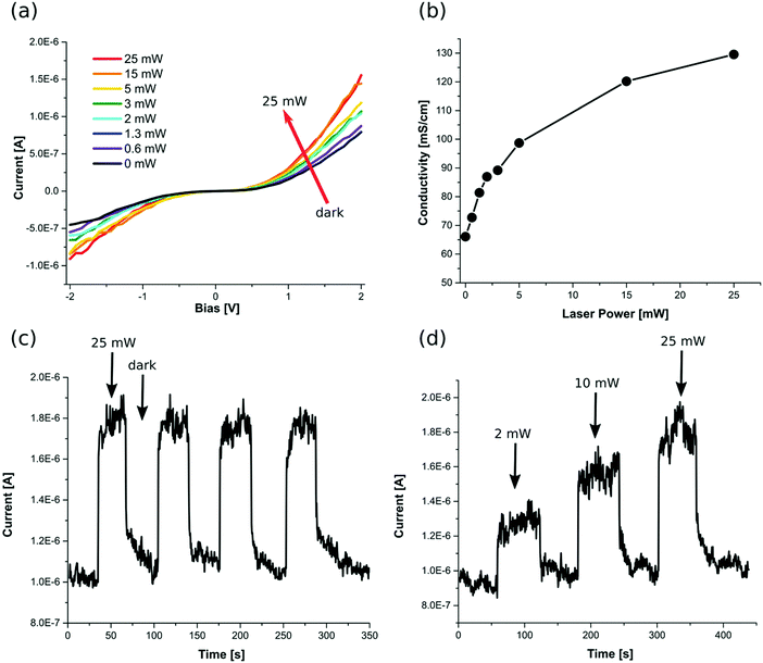 |
| | Fig. 8 The photo-electrical properties of the nanosheets: (a) I–V characteristics of the NSs in the dark and under illumination with the red laser (λ = 627 nm) of various intensities. Higher currents are achieved under illumination of higher powers (b) conductivity of the sheets in different laser powers. The photoconductivity increases upon increasing the power and saturates in higher powers. (c) Stability of the photo-current under intermittent illumination. By switching the 25 mW red laser on and off, stable photo-currents are achieved with fast transitions between the on-state and the off-state. (d) Intermittent illumination of the sheets with different powers. The photo-current can be tuned by the laser power, while the stability and the speed of the system are maintained. | |
In these equations, Iph is the photogenerated current, Plight is the laser power density (50 mW cm−1), A is the effective area of the device (0.5 μm2), and e is the elementary charge. The photodetectors based on our NSs exhibit a spectral response of ∼3 × 10³ AW−1 and a detectivity of ∼4 × 10⁹ Jones. The performance of these NSs is superior compared to previously reported works on this material under similar conditions.40 This is another proof for the high quality of the crystals and its low defect density.
Upon increasing the beam power, higher photocurrents are detected which are due to higher amounts of electron–hole pairs. However, as can be seen in Fig. 8b, the dependence of photoconductivity on the beam power experiences saturation in higher intensities. Upon intermittent illumination, we also demonstrate the stability of the photocurrent. Similar values are achieved for the photoconductivity under 25 mW illumination. Fast transitions between the on state and the off or dark state are observed (Fig. 8c), which is an important requirement for photo-detectors. This is a further indicator for the high quality of the crystals and the lack of defects.41 Also, using such measurements, a clear change in the photocurrent can be observed by changing the beam power, while stability and speed of the system remain unchanged (Fig. 8d). These measurements illustrate the potential of the produced SnS NSs for cost-effective non-toxic optoelectronics (e.g. photo-detectors).
Conclusion
A facile and simple colloidal method has been explored to synthesize large single-crystalline SnS NSs (size of 150–1680 nm and thickness of 16–50 nm) in the presence of oleic acid and trioctylphosphine as co-ligands together with two precursors, tin acetate and thioacetamide. Therefore, no metal halides (e.g. tin chloride) or flammable organo-metallic precursors are introduced. The two ligands OA (also oleate) and TOP are discovered to play a critical role in tuning the shape and size of the SnS NSs in addition to the original ligand, the acetate. The development of the final product involves the steps of instantaneous nucleation and anisotropic growth by the optimized balance of involved ligands. The NSs undergo a shape change between hexagonal sheets and square-like sheets by tuning their ligand quantity (acetate, oleate, OA, and TOP). The crystal phase can be optimized from PT structures (coming from nanoparticle byproducts) and OR crystal structures (coming from nanosheets) into single-crystalline nanosheets of OR structures only. The conductivity and photoconductivity measurements demonstrate their high potential for optoelectronic applications such as photo-sensors and photo-switches.
Conflicts of interest
There are no conflicts to declare.
Acknowledgements
The authors gratefully acknowledge financial support of the European Research Council via the ERC Starting Grant “2D-SYNETRA” (Seventh Framework Programme FP7, Project: 304980) and the China Scholarship Council (CSC), PRC. C. K. thanks the German Research Foundation DFG for financial support in the frame of the Cluster of Excellence “Center of ultrafast imaging CUI” and the Heisenberg scholarship KL 1453/9-2. We thank Stefan Werner (Universität Hamburg) for help with the HRTEM measurements.
References
- R. Lv, J. A. Robinson, R. E. Schaak, D. Sun, Y. Sun, T. E. Mallouk and M. Terrones, Acc. Chem. Res., 2014, 48, 56–64 CrossRef PubMed.
- H. Huang, Y. Cui, Q. Li, C. Dun, W. Zhou, W. Huang, L. Chen, C. A. Hewitt and D. L. Carroll, Nano Energy, 2016, 26, 172–179 CrossRef.
- F. Niu, J. Yang, N. Wang, D. Zhang, W. Fan, J. Yang and Y. Qian, Adv. Funct. Mater., 2017, 27 Search PubMed.
- Y. Tang, Z. Zhao, Y. Wang, Y. Dong, Y. Liu, X. Wang and J. Qiu, ACS Appl. Mater. Interfaces, 2016, 8, 32324–32332 CrossRef PubMed.
- O. C. Compton and F. E. Osterloh, J. Phys. Chem. C, 2008, 113, 479–485 CrossRef.
- A. Takagaki, M. Sugisawa, D. Lu, J. N. Kondo, M. Hara, K. Domen and S. Hayashi, J. Am. Chem. Soc., 2003, 125, 5479–5485 CrossRef PubMed.
- D. Voiry, J. Yang and M. Chhowalla, Adv. Mater., 2016, 28, 6197–6206 CrossRef PubMed.
- H. S. Im, Y. Myung, K. Park, C. S. Jung, Y. R. Lim, D. M. Jang and J. Park, RSC Adv., 2014, 4, 15695–15701 RSC.
- G. B. Bhandari, K. Subedi, Y. He, Z. Jiang, M. Leopold, N. Reilly, H. P. Lu, A. T. Zayak and L. Sun, Chem. Mater., 2014, 26, 5433–5436 CrossRef.
- Y. Peng, L. Shang, T. Bian, Y. Zhao, C. Zhou, H. Yu, L.-Z. Wu, C.-H. Tung and T. Zhang, Chem. Commun., 2015, 51, 4677–4680 RSC.
- W.-k. Koh, N. K. Dandu, A. F. Fidler, V. I. Klimov, J. M. Pietryga and S. V. Kilina, J. Am. Chem. Soc., 2017, 139, 2152–2155 CrossRef PubMed.
- J. S. Son, K. Park, S. G. Kwon, J. Yang, M. K. Choi, J. Kim, J. H. Yu, J. Joo and T. Hyeon, Small, 2012, 8, 2394–2402 CrossRef PubMed.
- W. J. Baumgardner, J. J. Choi, Y.-F. Lim and T. Hanrath, J. Am. Chem. Soc., 2010, 132, 9519–9521 CrossRef PubMed.
- D. Sun and R. E. Schaak, Chem. Mater., 2016, 29, 817–822 CrossRef.
- F. Ke, J. Yang, C. Liu, Q. Wang, Y. Li, J. Zhang, L. Wu, X. Zhang, Y. Han and B. Wu, J. Phys. Chem. C, 2013, 117, 6033–6038 CrossRef.
- A. J. Biacchi, D. D. Vaughn and R. E. Schaak, J. Am. Chem. Soc., 2013, 135, 11634–11644 CrossRef PubMed.
- A. Rabkin, S. Samuha, R. E. Abutbul, V. Ezersky, L. Meshi and Y. Golan, Nano Lett., 2015, 15, 2174–2179 CrossRef PubMed.
- N. Koteeswara Reddy, M. Devika and E. Gopal, Crit. Rev. Solid State Mater. Sci., 2015, 40, 359–398 CrossRef.
- H. Wiedemeier, H. Georg and G. V. Schnering, Z. Kristallogr. - Cryst. Mater., 1978, 148, 295–304 CrossRef.
- A. Rodin, L. C. Gomes, A. Carvalho and A. C. Neto, Phys. Rev. B, 2016, 93, 045431 CrossRef.
- S. Lin, A. Carvalho, S. Yan, R. Li, S. Kim, A. Rodin, L. Carvalho, E. M. Chan, X. Wang and A. H. C. Neto, Nat. Commun., 2018, 9, 1455 CrossRef PubMed.
- J. Xia, X.-Z. Li, X. Huang, N. Mao, D.-D. Zhu, L. Wang, H. Xu and X.-M. Meng, Nanoscale, 2016, 8, 2063–2070 RSC.
- S. Vishwanath, X. Liu, S. Rouvimov, L. Basile, N. Lu, A. Azcatl, K. Magno, R. M. Wallace, M. Kim and J.-C. Idrobo, J. Mater. Res., 2016, 31, 900–910 CrossRef.
- J. R. Brent, D. J. Lewis, T. Lorenz, E. A. Lewis, N. Savjani, S. J. Haigh, G. Seifert, B. Derby and P. O’Brien, J. Am. Chem. Soc., 2015, 137, 12689–12696 CrossRef PubMed.
- J. Tang and E. H. Sargent, Adv. Mater., 2011, 23, 12–29 CrossRef PubMed.
- D. V. Talapin, J.-S. Lee, M. V. Kovalenko and E. V. Shevchenko, Chem. Rev., 2009, 110, 389–458 CrossRef PubMed.
- X.-L. Gou, J. Chen and P.-W. Shen, Mater. Chem. Phys., 2005, 93, 557–566 CrossRef.
- B. K. Patra, S. Sarkar, A. K. Guria and N. Pradhan, J. Phys. Chem. Lett., 2013, 4, 3929–3934 CrossRef.
- A. de Kergommeaux, M. Lopez-Haro, S. Pouget, J.-M. Zuo, C. Lebrun, F. Chandezon, D. Aldakov and P. Reiss, J. Am. Chem. Soc., 2015, 137, 9943–9952 CrossRef PubMed.
- X. Liu, Y. Li, B. Zhou, X. Wang, A. N. Cartwright and M. T. Swihart, Chem. Mater., 2014, 26, 3515–3521 CrossRef.
- D. D. Vaughn, S.-I. In and R. E. Schaak, ACS Nano, 2011, 5, 8852–8860 CrossRef PubMed.
- M. M. Kobylinski, C. Ruhmlieb, A. Kornowski and A. Mews, J. Phys. Chem. C, 2018, 122, 5784–5795 CrossRef.
- Y. Zhang, J. Lu, S. Shen, H. Xu and Q. Wang, Chem. Commun., 2011, 47, 5226–5228 RSC.
-
S. Kudera, L. Carbone, L. Manna and W. J. Parak, Semiconductor nanocrystal quantum dots, Springer, 2008, pp. 1–34 Search PubMed.
- R. Li, X. Zhang, H. Dong, Q. Li, Z. Shuai and W. Hu, Adv. Mater., 2016, 28, 1697–1702 CrossRef PubMed.
- Z. Deng, D. Han and Y. Liu, Nanoscale, 2011, 3, 4346–4351 RSC.
- C. Gao, H. Shen and L. Sun, Appl. Surf. Sci., 2011, 257, 6750–6755 CrossRef.
- V. S. Stafeeva, A. S. Mitiaev, A. M. Abakumov, A. A. Tsirlin, A. M. Makarevich and E. V. Antipov, Polyhedron, 2007, 26, 5365–5369 CrossRef.
- T. Bielewicz, S. Dogan and C. Klinke, Small, 2015, 11, 826–833 CrossRef PubMed.
- J. Wang, G. Lian, Z. Xu, C. Fu, Z. Lin, L. Li, Q. Wang, D. Cui and C. P. Wong, ACS Appl. Mater. Interfaces, 2016, 8, 9545–9551 CrossRef PubMed.
- Z. Deng, D. Cao, J. He, S. Lin, S. M. Lindsay and Y. Liu, ACS Nano, 2012, 6, 6197–6207 CrossRef PubMed.
Footnote |
| † Electronic supplementary information (ESI) available: Further experimental data are presented. In particular, detailed TEM images of the shape and crystallographic structure of the nanosheets, AFM images to determine the height of the materials, and XRD measurements to determine the crystallographic phase. Further, SEM results are shown. See DOI: 10.1039/c8tc02559b |
|
| This journal is © The Royal Society of Chemistry 2018 |
Click here to see how this site uses Cookies. View our privacy policy here. 
 Open Access Article
 This Open Access Article is licensed under a Creative Commons Attribution-Non Commercial 3.0 Unported Licence
 a,
Mohammad Mehdi
Ramin Moayed
a,
Frauke
Gerdes
a,
Sascha
Kull
a,
Eugen
Klein
a,
Rostyslav
Lesyuk
ab and
Christian
Klinke
a,
Mohammad Mehdi
Ramin Moayed
a,
Frauke
Gerdes
a,
Sascha
Kull
a,
Eugen
Klein
a,
Rostyslav
Lesyuk
ab and
Christian
Klinke