Enhanced thermoelectric performance of Sn-doped Cu3SbS4†
Received
22nd May 2018
, Accepted 23rd June 2018
First published on 1st August 2018
Abstract
Cu3SbS4 is an earth-abundant and low-cost alternative thermoelectric material for medium temperature applications. Tin doping into Cu3SbS4 yields materials with high thermoelectric performance. The electronic structure of Sn-doped Cu3SbS4 was studied using both hybrid density functional theory (DFT) and the quasi-particle self-consistent GW (QSGW) approach. A synthesis method involving mechanical alloying (MA) and spark plasma sintering (SPS) was employed to produce dense and single phase Cu3SbS4 samples with very fine grain size. Previously unreported nano-scale twins on {112} planes were observed by transmission electron microscopy (TEM). All of the samples showed very low lattice thermal conductivity, which is attributed to their microstructures. Sn was found to substitute Sb successfully in Cu3SbS4 and work effectively as an acceptor dopant, leading to an enhanced power factor. A maximum zT value of 0.72 at 623 K was achieved in Cu3Sb1−xSnxS4 (x = 0.05), which is comparable to the Se analogue Cu3SbSe4.
1. Introduction
Global energy production is subject to considerable losses every year, mainly in the form of waste heat.1 Finding an effective way to harvest waste heat is of great importance to mitigate the rising issues related to energy resources and the environment. Thermoelectric generators (TEGs) based on the Seebeck effect can directly convert waste heat into electricity from a wide variety of heat sources.2 Unlike traditional heat pumps, TEGs are solid-state devices which are reliable, compact and emission-free. Currently, their applications are very restricted due to their relatively low conversion efficiency and high-cost. The conversion efficiency of a TEG is primarily determined by the dimensionless figure-of-merit, zT = α2ρ−1κ−1T, of the constituent thermoelectric (TE) material, where T is the absolute temperature, α is the Seebeck coefficient, ρ is the electrical resistivity, and κ is the thermal conductivity.2–5 In order to make a cost-effective TEG for the mass market, continuous efforts are being made to push up the zT value of known systems, but most of the good thermoelectric materials contain toxic, expensive and rare elements. Thus, exploring new TE materials from the viewpoints of low-cost, low-toxicity and earth-abundance is drawing increasing attention. In recent years, Cu-based sulfides, such as Cu12Sb4S13,6–8 Cu3SbS4,9–11 CuSbS2,12,13 CuCr2S4,14 Cu2SnS3,15,16 Cu3SnS4,17 CuFeS2,18–21 Cu5FeS4,22 Cu6Fe2SnS8,23 have been recognized as interesting and promising TE materials. Among these compounds, Cu3SbS4 has a simple zinc-blende related structure with a moderate band gap of ∼0.47 eV.24 It shows a large effective mass derived from its degenerate bands, which is favourable for high thermoelectric performance.25 In our previous work, a combined theoretical and experimental study of Cu3SbS4 revealed its low thermal conductivity and promising TE performance.9 The zT value of Cu3SbS4 was enhanced by Ge-doping on the Sb site, however, a competitive second phase of Cu2GeS3 was formed even at a very low dopant concentration (∼1.25%). To further explore the potential TE properties of Cu3SbS4, we report here a detailed study of Sn-doped Cu3SbS4. Although Sn has been previously reported as dopant in Cu3SbS4,11 a complex solid-reaction method was used and the samples contained SnO2 impurity and large voids (1 μm). A poor maximum zT value of 0.1 was obtained at 573 K. Based on our previous work on Cu3SbS4 and the reports on its analogue Cu3SbSe4,26,27 a better TE performance is expected for Sn-doped Cu3SbS4. Sn4+ and Sb5+ have similar ionic radii and Sn has one less valence electron than Sb, which suggests that Sn should be a good acceptor dopant in Cu3SbS4. In this work, we demonstrate high TE performance in Sn-doped Cu3SbS4 prepared by a combination of mechanical alloying (MA) and spark plasma sintering (SPS). This simple method produced samples of high-quality, high-purity and fine microstructures. Sn successfully substituted Sb and worked as a very effective p-type dopant in Cu3SbS4. This is further confirmed by detailed electronic structure calculations performed with hybrid DFT and validated with Quasi-particle Self-consistent GW (QSGW) calculations. Microstructural analysis reveals nano-twinning defects in Cu3SbS4, which have not previously been reported.
2. Experimental
2.1 Synthesis and characterization
Polycrystalline Cu3Sb1−xSnxS4 samples with nominal compositions corresponding to x = 0.00, 0.01, 0.03, 0.05, 0.10 and 0.15 were prepared by MA + SPS. Starting powders of Cu (99.5%, AlfaAesar), Sb (99.5%, AlfaAesar), Sn (99.999%, AlfaAesar), and S (reagent grade, purified by sublimation, Sigma-Aldrich) were loaded into a stainless steel jar with stainless steel balls and sealed in an inert atmosphere of argon. The powder mixture was milled at a rotation speed of 420 rpm for 20 h in a planetary ball mill machine (QM-3SP2, Nanjing University, China). The as-synthesized powders were sintered at 723 K for 3 min at a pressure of 50 MPa using an SPS furnace (FCT HPD 25, FCT System GmbH, Germany). The phases of the samples were examined using X-ray powder diffraction (XRD, PANalytical X'Pert Pro, Cu-Kα). The microstructures were observed using scanning electron microscopy (SEM, FEI, Inspect F, 10 kV) and transmission electron microscopy (TEM, Jeol JEM 2010, 200 kV). SEM images were taken of freshly fractured surfaces and TEM images were taken of the crushed powders. Bars of 3 mm × 3 mm × 15 mm were cut from the samples using a diamond saw for electrical resistivity (ρ) and Seebeck coefficient (α) measurements, which were performed using a ZEM-3 (ULVAC-RIKO, Japan) from ambient temperature to 623 K. The uncertainty of resistivity and Seebeck coefficient values is less than 5%. The room temperature Hall coefficient (RH) was measured using the Van der Pauw method (The Lake Shore 8400 Series HMS). The carrier concentration (n) was calculated as n = 1/eRH. The uncertainty of the Hall measurement increased with increasing conductivity of the sample and the largest uncertainty was estimated to be 10%. Thermal diffusivity was measured using the flash diffusivity method (LFA 457, Netzsch) up to 623 K. The specific heat capacity (Cp) was determined by a comparative method in the LFA 457, using Pyroceram 9606 as a reference sample. The uncertainty of thermal diffusivity and heat capacity measurements was less than 5%. The density was measured using the Archimedes method with an uncertainty of less than 1% and all the samples had a relative density greater than 98%. The thermal conductivity was calculated using the thermal diffusivity, specific heat capacity and density.
2.2 Computational methods
The theoretical calculations were performed within the density functional theory (DFT) using the projector augmented wave method (PAW) as implemented in the Vienna ab initio simulation package (VASP).28,29 The screened hybrid functional of Heyd, Scuseria and Ernzerhof (HSE06) and spin–orbit effects were also included in the calculations.30–33 A primitive cell of 8 atoms was used to describe the Cu3SbS4 crystal structure, while a supercell of 64 atoms (2 × 2 × 2) was built to model Sn-doped Cu3Sb1−xSnxS4 (x = 0.125), with a Sn atom substituted for an Sb atom. The Seebeck coefficient was computed within the constant relaxation time approximation using the Wannier interpolation scheme implemented in the BoltzWann code.34 Doping was simulated via a shift of the chemical potential. In order to benchmark the electronic structures obtained with HSE06, the band structure of Cu3SbS4 was also calculated with quasi-particle self-consistent GW (QSGW) as implemented in the Questaal package (The QUESTAAL code is freely available at http://www.questaal.org.), within a Full Potential Linear Muffin-Tin Orbital (FP-LMTO) framework.35–37 The smoothed LMTO basis used in this work includes atomic orbitals with l ≤ lmax = 4, with 4d orbitals of Sb and Cu added in the form of local orbitals. Since QSGW gives the self-consistent solution at the scalar relativistic level, we account for the spin–orbit coupling adding the operator HSO = L·S/2c2 as a perturbation not included in the self-consistency cycle. The QSGW calculations were performed using the HSE06 relaxed structure of Cu3SbS4.
3. Results and discussion
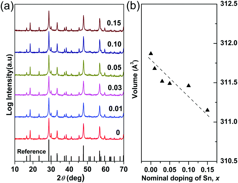
The X-ray powder diffraction patterns for the compositions studied in the Cu3Sb1−xSnxS4 system are shown in Fig. 1a. All of the compositions are phase pure (within the limits of the technique), exhibiting the tetragonal structure of Cu3SbS4 (PDF 00-035-0581). The unit cell volume generally decreased (Fig. 1b) with increasing x-value although the volume change is very small (less than 0.4%). According to Shannon,38 the radius for tetrahedral Sn4+ in a chalcogenide is 0.55 Å. Unfortunately, the corresponding value for Sb5+ is not recorded. However, using the reported Sb–S interatomic distance (2.405 Å) in Cu3SbS439 and the Shannon ionic radius of S2− (1.84 Å), the radius of Sb5+ in a tetrahedral coordination is calculated to be 0.565 Å. Thus the decrease in unit cell volume appears to be consistent with substitution of Sb5+ by Sn4+ on the tetrahedral sites.
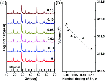 |
| | Fig. 1 (a) XRD patterns and (b) compositional variation of unit cell volume in Cu3Sb1−xSnxS4 system. | |
To gain further insight into the solubility as well as the structural effects related to Sn-doping, a theoretical analysis was performed using DFT. The lattice parameters of tetragonal Cu3SbS4 obtained with DFT are a = 5.41 Å and c = 10.80 Å, which are in close agreement with the experimental data (a = 5.39 Å, c = 10.75 Å). A model of Cu3Sb0.875Sn0.125S4 (x = 0.125) was built to illustrate the effects of Sn-doping. The calculated volume of Cu3Sb0.875Sn0.125S4 was contracted by 0.4% with respect to the undoped Cu3SbS4, which is consistent with the experimental results. The calculated formation energy of the SnSb defect is −0.61 eV, showing that solubility of Sn in Cu3SbS4 is energetically favourable. The formation energy obtained here is quite close to the formation energy of GeSb defects in Cu3SbS4 (−0.68 eV).9 However, it is important to point out that, contrary to the case of Ge substitution, here the local restructuring around the Sn atom is very small (the Sn–Cu distances contract by about 0.4% and the Sn–S distances expand by about 0.5% upon relaxation from the pristine Cu3SbS4 geometry), which is in line with the good solubility observed experimentally.
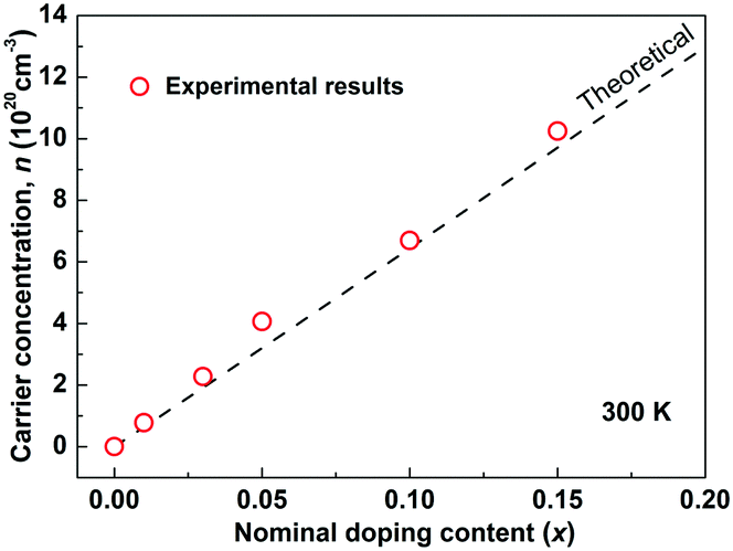
As Sb5+ is substituted by Sn4+, each Sn is expected to donate one hole in Cu3SbS4 by electronic compensation. Based on this assumption, the theoretical carrier concentration was calculated according to the nominal doping content, and is shown as the dashed line in Fig. 2. The measured carrier concentrations are shown as red circles, showing good consistency between the theoretical and the experimental results. This further suggests that Sn completely substitutes for Sb in Cu3SbS4. In fact, a complete solid-solution of Cu3SbS4–Cu3SnS4 was successfully prepared. The samples with high Sn-content are very conductive and exhibit poor thermoelectric performance and therefore not included in this work. However, the mechanisms and effects of this high solubility might provide a more insightful understanding of Cu3SbS4 and related compounds such as Cu2ZnSnS4 (Kesterite), and this part is of a parallel investigation.40
 |
| | Fig. 2 Carrier concentration as a function of the nominal doping content at room temperature in Cu3Sb1−xSnxS4 system. The dashed line is the theoretical model where a full charge transfer is assumed (one hole carrier per dopant). | |
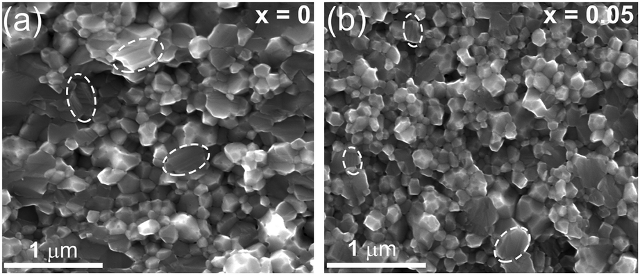
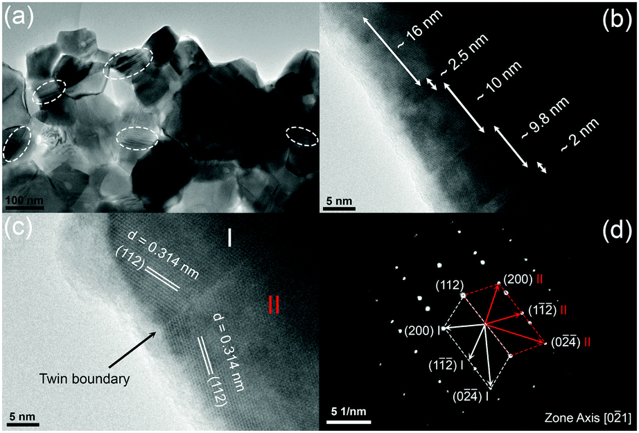
Fig. 3 shows typical fracture surfaces of the undoped and Sn-doped samples. Both transgranular and intergranular fractures are observed. The samples have very fine grains and the grain size estimated from SEM of fracture surfaces is about 50 nm to 400 nm, which is much smaller than the reported grain size of 3 to 10 μm of Cu3SbS4 prepared by solid state reaction.10 According to previous reports, these nanoscale grains and mesoscale grains in Cu3SbS4 can effectively scatter phonons with medium- and long-wavelengths.41–43 Looking closely at the microstructures, some striation-like defects were observed on the transgranular fractured grains for both undoped and doped samples and these were examined by TEM. Fig. 4a shows a representative low magnification TEM image of Cu3SbS4, and the striation-like defects can be seen more clearly. These defects were identified as being due to crystal twining from high resolution transmission electron microscopy (HRTEM) images. A series of twin bands with thickness from ∼2 nm to ∼16 nm can be seen in Fig. 4b. Fig. 4c shows the typical twin structure of two domains with mirror symmetry and the measured d-spacing of domain I and domain II are approximately 0.314 nm, consistent with the (112) planes in the XRD data of Cu3SbS4. A corresponding selected area electron diffraction (SAED) pattern is shown in Fig. 4d. Two sets of symmetric electron diffraction spots were observed in the pattern along the [0−21] zone axis, and the twin planes are confirmed as {112} planes. Similar twinning defects were also found in the Sn-doped samples (see Fig. S1 in ESI†). The TEM analysis is consistent with the reported twinning structures in Cu2ZnSnS4, which has a similar tetragonal zinc blende related structure to Cu3SbS4.44,45 The twinning structures reported in InSb and ZnS with cubic zinc blende structure, are on the {111} close-packed planes.46,47 These results are also consistent as the {112} planes in Cu3SbS4 are equivalent to the {111} planes in the cubic lattice. The above microstructural features of Cu3SbS4 were not noticed in our previous work9 and have not been reported by others. There is, in fact, very limited research on the effects of nano-twinning in TE materials. The nano-twinning defects in Cu3SbS4 are most likely to be deformation twins. As the samples were prepared by MA + SPS, the high energy collisions in MA and the fast sintering with high pressure in SPS could all contribute to the formation of these defects. When considering the impact of nano-twinning on the transport properties, the twin boundary can be regarded as a coherent boundary with atomic structure close to the perfect crystal.42,48,49 Compared to an incoherent grain boundary, a coherent twin boundary is less effective in scattering phonons, but has far less effect on carrier transport.50–52 It is rationalized that a high density of twin boundaries can introduce noticeable additional scattering of phonons with nearly unaffected electrical transport.
 |
| | Fig. 3 Representative SEM images of fractured surface for Cu3Sb1−xSnxS4, (a) x = 0, (b) x = 0.05. Striation-like defects were observed on the transgranular fracture of the grains. | |
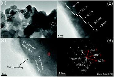 |
| | Fig. 4 Representative TEM images for Cu3SbS4, (a) low magnification image, (b and c) HRTEM images with twinning superlattice, and (d) corresponding SAED pattern. | |
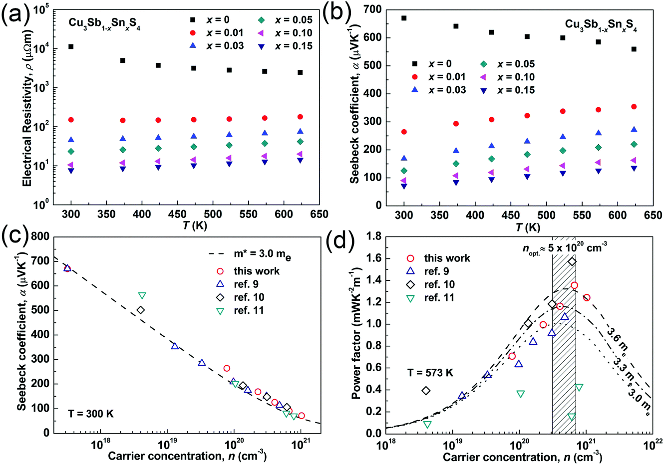
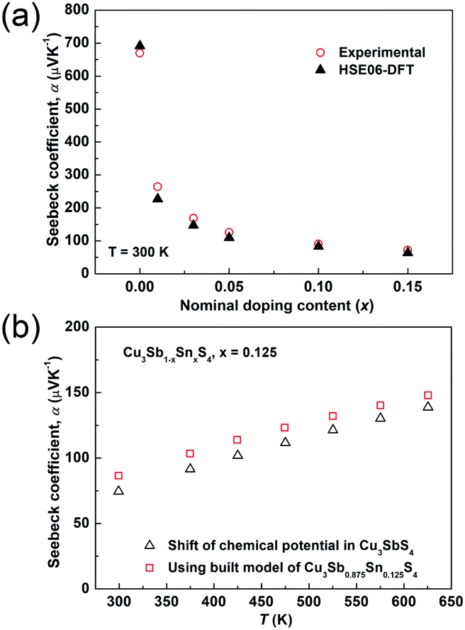
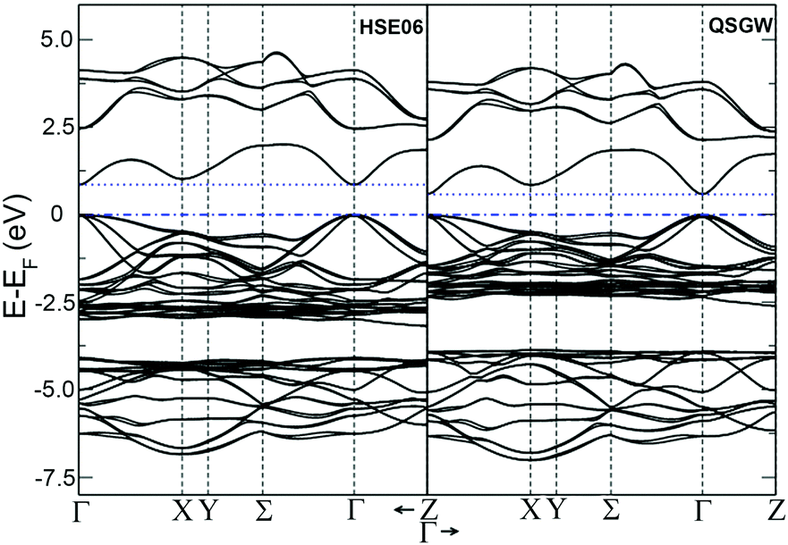
The temperature dependences of the electrical resistivity (ρ) and Seebeck coefficient (α) are shown in Fig. 5a and b, respectively. The undoped Cu3SbS4 sample has a carrier concentration (n) of 3.2 × 1017 cm−3 at room temperature and showed semiconducting behavior with a large electrical resistivity and Seebeck coefficient, both of which decreased with increasing temperature. The electrical resistivities of Sn-doped samples were significantly reduced due to the increased carrier concentration (Fig. 2) and consequently, their Seebeck coefficients decreased. All of the Sn-doped samples exhibited metal-like behavior, and the electrical resistivity and Seebeck coefficient increased with increasing temperature. This is opposite to the trend seen in the undoped sample. Fig. 5c shows the carrier concentration dependence of the Seebeck coefficient at 300 K, including previously reported data for Cu3SbS4.9–11 A single parabolic band (SPB) model was used to evaluate the transport properties (see ESI† for SPB calculations)53 and the dashed line represents calculated results with a density of state (DOS) effective mass (m*) of 3.0 me. The results show very good consistency, indicating a large effective mass in Cu3SbS4 despite the different doping levels. The power factor was greatly enhanced with Sn-doping, and a maximum power factor of 1.35 mW K−2 m−1 was obtained at 573 K for x = 0.1 sample. To identify the optimum carrier concentration (nopt.), the carrier concentration dependence of the power factor at 573 K is shown in Fig. 5d, assuming the carrier concentration is constant with increasing temperature. The experimental results are very close to the SPB predictions with effective mass of 3.0 me to 3.6 me, indicating an optimum carrier concentration around 5 × 1020 cm−3. The power factor reported by Goto et al. (ref. 11) is much lower, which was probably caused by the second phase of SnO2 in their material.11 The optimum carrier concentration corresponding to the maximum power factor and the effective mass m* of Sn-doped Cu3SbS4 identified in this work match well with the empirical relationship of nopt. ∝ m*.54,55Fig. 6a shows the theoretical values of the Seebeck coefficient obtained from the HSE06-DFT bands of pristine Cu3SbS4, which are in very good agreement with the experimental data and consistent with our previous DFT+U calculations.9 It is important to point out that, as shown in Fig. 6b, the simple model for doping based on the electronic bands of Cu3SbS4 and a shift of the chemical potential gives results in good agreement with the ones obtained using the built model of Cu3Sb0.875Sn0.125S4, thus providing a clear validation of the theoretical approach. The choice of the HSE06 hybrid functional offers a way to bypass the need to use the adjustable U parameter of DFT+U, while retaining excellent structural and electronic properties.32,56–58 To show this, the accuracy of the HSE06 results were ultimately assessed against state-of-the-art QSGW calculations. Fig. 7 shows the electronic band structures of Cu3SbS4 calculated by both methods. The top of the valence band (the part that determines the transport properties of the p-doped compounds) is very similar in the two calculations: for instance, the density of states effective mass, m*, (computed neglecting spin–orbit coupling) is 2.2 me using HSE06 and 2.4 me using QSGW, confirming the DFT+U prediction of a high m* to explain the favorably large Seebeck coefficient in this compound.9 We notice that the spin–orbit coupling leads to a relatively small splitting of the degenerate bands at the valence band maximum (the splitting is 0.06 eV in QSGW and 0.03 eV in DFT). For completeness, it is important to point out that the two band structures also present noticeable differences. First, the valence band from the HSE06 calculations appears broader in energy than that from QSGW, because the fraction of non-local exchange in HSE06 generally tends to stretch the density of states over a wider range of energies.59 Secondly, and more importantly, the predicted band gap from HSE06 (Eg = 0.85 eV) is larger than that from QSGW band gap (Eg = 0.58 eV). The latter is closer to the experimental value of ∼0.47 eV.24 These differences are, however, not expected to affect our prediction for the Seebeck coefficient of Cu3SbS4 compound in the region of different doping levels.
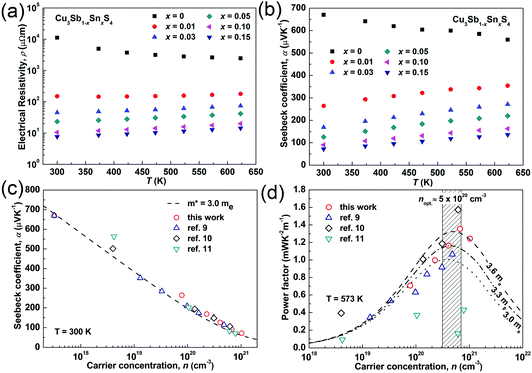 |
| | Fig. 5 (a) Electrical resistivity and (b) Seebeck coefficient as functions of temperature; (c) Seebeck coefficient and (d) power factor as functions of carrier concentration in Cu3Sb1−xSnxS4 system. | |
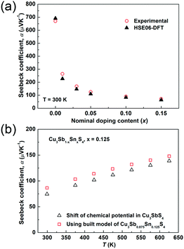 |
| | Fig. 6 (a) Comparison of experimental and theoretical Seebeck coefficients in the Cu3Sb1−xSnxS4 system at 300 K. The doping was simulated via a shift of chemical potential based on the Cu3SbS4 structure. (b) The calculated Seebeck coefficient of Cu3Sb1−xSnxS4 (x = 0.125) as a function of temperature. Open triangles represent the results based on the Cu3SbS4 structure with a shift of the chemical potential and open squares represent the results based on the built model of Cu3Sb0.875Sn0.125S4. | |
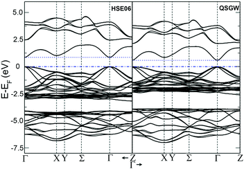 |
| | Fig. 7 Band structure for Cu3SbS4 for spin–orbit coupling calculation with hybrid-DFT (HSE06, left panel) and QSGW (right panel). All the energies in eV referred to the Fermi energy. | |
Fig. 8a and b show the temperature dependence of the thermal conductivities (κ) and lattice thermal conductivities (κL). For all of the samples, the thermal conductivity decreased with increasing temperature and there was no sign of bipolar effects over the investigated temperature range. With increasing Sn doping, the thermal conductivity increased due to the increased electronic contribution. The lattice thermal conductivity was calculated by subtracting the electronic contribution from the thermal conductivity. The Lorenz numbers were calculated based on the SPB model (see Fig. S2 in ESI†). As seen in Fig. 8b, all of the samples in the present work have similar lattice thermal conductivity and follow a T−1 trend, suggesting that thermal conduction is limited by Umklapp scattering and Sn-doping has little impact on lattice thermal conductivity.60 Compared to the reported results for Cu3SbS4,10,11,26 the sample prepared in this work shows a very low lattice thermal conductivity, which is more than two times lower at room temperature. It is even lower than that reported in its analogue Cu3SbSe4.27 This greatly reduced lattice thermal conductivity can be attributed to the unique microstructures of the materials produced in the current work. The extra phonon scattering is from the high density of grain boundaries created by the nanoscale and mesoscale grains, while the previously reported samples had microscale grains. The grain boundaries can effectively scatter medium- and long-wavelength phonons. The nano-twinning boundaries could also contribute to the low lattice thermal conductivity in Cu3SbS4, although it was reported to be less effective at phonon scattering than grain boundaries in several high thermal conductivity systems, such as diamond and Si.50,51 As all the samples in the present study have similar microstructures, we are not able to clarify the individual effect from grain boundaries and nano-twinning boundaries in this work. Nevertheless, it is worth paying more attention to the microstructures of compounds with similar structures. Fig. 8c shows the temperature dependence of the figure-of-merit, zT. The zT values exhibit a linearly increasing trend with increasing temperature for all of the samples. A maximum zT value of 0.72 was obtained at 623 K in the x = 0.05 sample. It is the highest zT value ever reported for a Cu3SbS4 based compound, which is comparable or even higher than the reported value of the Se analogue Cu3SbSe4.27,61–65
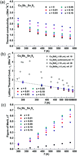 |
| | Fig. 8 (a) Thermal conductivity, (b) lattice thermal conductivity and (c) zT values of as functions of temperature in Cu3Sb1−xSnxS4 system. | |
4. Conclusions
Sn-Doping in Cu3SbS4 leads to a solid solution of general formula Cu3Sb1−xSnxS4. High density samples were prepared by a combination of mechanical alloying and spark plasma sintering, yielding high purity, dense materials with nanoscale and mesoscale grains (50 nm to 400 nm). Sn was found to have an exceptionally high solubility and work effectively as a p-type dopant in Cu3SbS4. The high x-value compositions are the subject of further work. Interesting twinning defects on {112} planes with nanoscale separation were found in Cu3SbS4 samples, which have not previously been reported. The electronic structure of this compound was carefully investigated using both HSE06-DFT and QSGW, and the calculated Seebeck coefficient was in very good agreement with the experimental results. A large effective mass (3.0 me) deriving from degenerate bands was found in Cu3SbS4, which is favorable for high thermoelectric performance. All of the samples in the present work exhibited very low lattice thermal conductivities, due mainly to the high density of grain boundaries. Considering the low lattice thermal conductivity of the samples, the nano-twinning defects are likely to impact on phonon transport. A maximum zT value of 0.72 at 623 K was achieved in the x = 0.05 sample with a carrier concentration of ∼4.1 × 1020 cm−3. This is the highest zT value reported for Cu3SbS4 system. Although the effects of twining boundaries on the electron and phonon transport is still not clear, more attention should be paid to nano-twinning in Cu3SbS4 and related compounds, as well as other thermoelectric materials.
Conflicts of interest
There are no conflicts to declare.
Acknowledgements
This work was supported by the Engineering and Physical Sciences Research Council (EPSRC) (Grant No. EP/N0227261/1 and EP/N02396X/1). N. B. and C. W. acknowledge the ARCHER UK National Supercomputing Service and the UK Materials and Molecular Modelling Hub for computational resources, which are partially funded by EPSRC (EP/P020194/1). N. B. also acknowledges the Cirrus UK National Tier-2 HPC Service at EPCC. N. B. and S. L. thank Mark van Schilfgaarde for helping with the QSGW calculations. C. W. and N. B. acknowledge Dr Glenn Jones (Johnson & Matthey, Sonning) for support and helpful discussions. C. W. gratefully acknowledges the support of NVIDIA Corporation with the donation of the Tesla K40 GPUs used in this research. Dr R. M. Wilson (QMUL) is thanked for his help in collecting XRD data.
Notes and references
- C. Forman, I. K. Muritala, R. Pardemann and B. Meyer, Renewable Sustainable Energy Rev., 2016, 57, 1568–1579 CrossRef.
-
D. M. Rowe, CRC Handbook of Thermoelectrics, CRC Press, 1995 Search PubMed.
-
G. S. Nolas, J. Sharp and H. J. Goldsmid, Thermoelectrics, 2001 Search PubMed.
- W. Liu, J. Hu, S. Zhang, M. Deng, C.-G. Han and Y. Liu, Mater. Today Phys., 2017, 1, 50–60 CrossRef.
- M. Takao, Small, 2017, 13, 1702013 CrossRef PubMed.
- S. Koichiro, T. Kojiro, A. Tomoki and K. Mikio, Appl. Phys. Express, 2012, 5, 051201 CrossRef.
- X. Lu, D. T. Morelli, Y. Xia, F. Zhou, V. Ozolins, H. Chi, X. Y. Zhou and C. Uher, Adv. Energy Mater., 2013, 3, 342–348 CrossRef.
- R. Chetty, A. Bali and R. C. Mallik, J. Mater. Chem. C, 2015, 3, 12364–12378 RSC.
- K. Chen, B. Du, N. Bonini, C. Weber, H. Yan and M. J. Reece, J. Phys. Chem. C, 2016, 120, 27135–27140 CrossRef.
- A. Suzumura, M. Watanabe, N. Nagasako and R. Asahi, J. Electron. Mater., 2014, 43, 2356–2361 CrossRef.
- Y. Goto, Y. Sakai, Y. Kamihara and M. Matoba, J. Phys. Soc. Jpn., 2015, 84, 044706 CrossRef.
- V. Kumar Gudelli, V. Kanchana, G. Vaitheeswaran, A. Svane and N. E. Christensen, J. Appl. Phys., 2013, 114, 223707 CrossRef.
- B. Du, R. Zhang, K. Chen, A. Mahajan and M. J. Reece, J. Mater. Chem. A, 2017, 5, 3249–3259 RSC.
- A. U. Khan, R. A. R. A. Orabi, A. Pakdel, J.-B. Vaney, B. Fontaine, R. Gautier, J.-F. Halet, S. Mitani and T. Mori, Chem. Mater., 2017, 29, 2988–2996 CrossRef.
- Y. W. Shen, C. Li, R. Huang, R. M. Tian, Y. Ye, L. Pan, K. Koumoto, R. Z. Zhang, C. L. Wan and Y. F. Wang, Sci. Rep., 2016, 6, 32501 CrossRef PubMed.
- H. Zhao, X. Xu, C. Li, R. Tian, R. Zhang, R. Huang, Y. Lyu, D. Li, X. Hu, L. Pan and Y. Wang, J. Mater. Chem. A, 2017, 5, 23267–23275 RSC.
- Y. Yang, P. Ying, J. Wang, X. Liu, Z. Du, Y. Chao and J. Cui, J. Mater. Chem. A, 2017, 5, 18808–18815 RSC.
- N. Tsujii and T. Mori, Appl. Phys. Express, 2013, 6, 043001 CrossRef.
- D. Berthebaud, O. I. Lebedev and A. Maignan, J. Materiomics, 2015, 1, 68–74 CrossRef.
- R. Ang, A. U. Khan, N. Tsujii, K. Takai, R. Nakamura and T. Mori, Angew. Chem., Int. Ed., 2015, 54, 12909–12913 CrossRef PubMed.
- H. Takaki, K. Kobayashi, M. Shimono, N. Kobayashi, K. Hirose, N. Tsujii and T. Mori, Mater. Today Phys., 2017, 3, 85–92 CrossRef.
- G. Guelou, A. V. Powell and P. Vaqueiro, J. Mater. Chem. C, 2015, 3, 10624–10629 RSC.
- R. Zhang, K. Chen, B. Du and M. J. Reece, J. Mater. Chem. A, 2017, 5, 5013–5019 RSC.
- K. I. Amirkhanov, G. G. Gadzhiev and Y. B. Magomedov, High Temp., 1978, 16, 1050–1052 Search PubMed.
- Y. Pei, X. Shi, A. LaLonde, H. Wang, L. Chen and G. J. Snyder, Nature, 2011, 473, 66–69 CrossRef PubMed.
- E. J. Skoug, J. D. Cain, D. T. Morelli, M. Kirkham, P. Majsztrik and E. Lara-Curzio, J. Appl. Phys., 2011, 110, 023501 CrossRef.
- T. Wei, H. Wang, Z. M. Gibbs, C. Wu, G. J. Snyder and J. Li, J. Mater. Chem. A, 2014, 2, 13527–13533 RSC.
- G. Kresse and D. Joubert, Phys. Rev. B: Condens. Matter Mater. Phys., 1999, 59, 1758–1775 CrossRef.
- G. Kresse and J. Hafner, Phys. Rev. B: Condens. Matter Mater. Phys., 1994, 49, 14251–14269 CrossRef.
- J. Heyd, G. E. Scuseria and M. Ernzerhof, J. Chem. Phys., 2006, 124, 219906 CrossRef.
- J. Heyd, G. E. Scuseria and M. Ernzerhof, J. Chem. Phys., 2003, 118, 8207–8215 CrossRef.
- J. Paier, M. Marsman, K. Hummer, G. Kresse, I. C. Gerber and J. G. Ángyán, J. Chem. Phys., 2006, 124, 154709 CrossRef PubMed.
- J. Paier, M. Marsman, K. Hummer, G. Kresse, I. C. Gerber and J. G. Ángyán, J. Chem. Phys., 2006, 125, 249901 CrossRef.
- G. Pizzi, D. Volja, B. Kozinsky, M. Fornari and N. Marzari, Comput. Phys. Commun., 2014, 185, 422–429 CrossRef.
- T. Kotani, M. van Schilfgaarde and S. V. Faleev, Phys. Rev. B: Condens. Matter Mater. Phys., 2007, 76, 165106 CrossRef.
- M. van Schilfgaarde, T. Kotani and S. Faleev, Phys. Rev. Lett., 2006, 96, 226402 CrossRef PubMed.
- M. van Schilfgaarde, T. Kotani and S. V. Faleev, Phys. Rev. B: Condens. Matter Mater. Phys., 2006, 74, 245125 CrossRef.
- R. Shannon, Acta Crystallogr., Sect. A: Cryst. Phys., Diffr., Theor. Gen. Crystallogr., 1976, 32, 751–767 CrossRef.
- J. Garin and E. Parthé, Acta Crystallogr., Sect. B: Struct. Crystallogr. Cryst. Chem., 1972, 28, 3672–3674 CrossRef.
-
C. D. Paola, K. Chen, I. Abrahams, N. Bonini, C. Weber, H. Yan and M. Reece, in preparation.
- K. Biswas, J. He, I. D. Blum, C. I. Wu, T. P. Hogan, D. N. Seidman, V. P. Dravid and M. G. Kanatzidis, Nature, 2012, 489, 414–418 CrossRef PubMed.
- G. J. Tan, L. D. Zhao and M. G. Kanatzidis, Chem. Rev., 2016, 116, 12123–12149 CrossRef PubMed.
- D. M. Rowe, V. S. Shukla and N. Savvides, Nature, 1981, 290, 765 CrossRef.
- B. Shin, Y. Zhu, T. Gershon, N. A. Bojarczuk and S. Guha, Thin Solid Films, 2014, 556, 9–12 CrossRef.
- N. Kattan, B. Hou, D. J. Fermín and D. Cherns, Appl. Mater. Today, 2015, 1, 52–59 CrossRef.
- Y. Qian and Q. Yang, Nano Lett., 2017, 17, 7183–7190 CrossRef PubMed.
- H. B. Ahn and J. Y. Lee, Mater. Lett., 2013, 106, 308–312 CrossRef.
- R. Aghababaei, G. Anciaux and J.-F. Molinari, Appl. Phys. Lett., 2014, 105, 194102 CrossRef.
- J. He, M. G. Kanatzidis and V. P. Dravid, Mater. Today, 2013, 16, 166–176 CrossRef.
- H. Dong, J. Xiao, R. Melnik and B. Wen, Sci. Rep., 2016, 6, 19575 CrossRef PubMed.
- H. F. Zhan, Y. Y. Zhang, J. M. Bell and Y. T. Gu, J. Phys. D: Appl. Phys., 2014, 47, 015303 CrossRef.
- L. Lu, Y. Shen, X. Chen, L. Qian and K. Lu, Science, 2004, 304, 422–426 CrossRef PubMed.
-
D. M. Rowe, Thermoelectrics and its energy harvesting, CRC Press, Boca Raton, FL, 2012 Search PubMed.
- C. Fu, S. Bai, Y. Liu, Y. Tang, L. Chen, X. Zhao and T. Zhu, Nat. Commun., 2015, 6, 8144 CrossRef PubMed.
- C. Fu, T. Zhu, Y. Liu, H. Xie and X. Zhao, Energy Environ. Sci., 2015, 8, 216–220 RSC.
- J. Paier, R. Asahi, A. Nagoya and G. Kresse, Phys. Rev. B: Condens. Matter Mater. Phys., 2009, 79, 115126 CrossRef.
- F. Fuchs, J. Furthmüller, F. Bechstedt, M. Shishkin and G. Kresse, Phys. Rev. B: Condens. Matter Mater. Phys., 2007, 76, 115109 CrossRef.
- M. Jain, J. R. Chelikowsky and S. G. Louie, Phys. Rev. Lett., 2011, 107, 216806 CrossRef PubMed.
- J. E. Northrup, M. S. Hybertsen and S. G. Louie, Phys. Rev. Lett., 1987, 59, 819–822 CrossRef PubMed.
- E. S. Toberer, A. Zevalkink and G. J. Snyder, J. Mater. Chem., 2011, 21, 15843 RSC.
- X. Y. Li, D. Li, H. X. Xin, J. Zhang, C. J. Song and X. Y. Qin, J. Alloys Compd., 2013, 561, 105–108 CrossRef.
- C. Yang, F. Huang, L. Wu and K. Xu, J. Phys. D: Appl. Phys., 2011, 44, 295404 CrossRef.
- E. J. Skoug, J. D. Cain, P. Majsztrik, M. Kirkham, E. Lara-Curzio and D. T. Morelli, Sci. Adv. Mater., 2011, 3, 602–606 CrossRef.
- D. Li, R. Li, X. Qin, C. Song, H. Xin, L. Wang, J. Zhang, G. Guo, T. Zou, Y. Liu and X. Zhu, Dalton Trans., 2014, 43, 1888–1896 RSC.
- D. Chen, Y. Zhao, Y. Chen, T. Lu, Y. Wang, J. Zhou and Z. Liang, Adv. Electron. Mater., 2016, 2, 1500473 CrossRef.
Footnote |
| † Electronic supplementary information (ESI) available. See DOI: 10.1039/c8tc02481b |
|
| This journal is © The Royal Society of Chemistry 2018 |
Click here to see how this site uses Cookies. View our privacy policy here. 
 Open Access Article
 This Open Access Article is licensed under a
  *a,
Cono
Di Paola
b,
Baoli
Du
c,
Ruizhi
Zhang
a,
Savio
Laricchia
b,
Nicola
Bonini
b,
Cedric
Weber
b,
Isaac
Abrahams
*a,
Cono
Di Paola
b,
Baoli
Du
c,
Ruizhi
Zhang
a,
Savio
Laricchia
b,
Nicola
Bonini
b,
Cedric
Weber
b,
Isaac
Abrahams