
 Open Access Article
 This Open Access Article is licensed under a Creative Commons Attribution-Non Commercial 3.0 Unported Licence
Enhancing the hydrophobicity of perovskite solar cells using C18 capped CH3NH3PbI3 nanocrystals†
Isabella
Poli
 *ab,
Xinxing
Liang
a,
Robert
Baker
ab,
Salvador
Eslava
bc and
Petra J.
Cameron
*ab
*ab,
Xinxing
Liang
a,
Robert
Baker
ab,
Salvador
Eslava
bc and
Petra J.
Cameron
*ab
aDepartment of Chemistry, University of Bath, Bath BA2 7AY, UK. E-mail: i.poli@bath.ac.uk; p.j.cameron@bath.ac.uk
bCentre for Sustainable Chemical Technologies, University of Bath, Bath BA2 7AY, UK
cDepartment of Chemical Engineering, University of Bath, Bath BA2 7AY, UK
First published on 16th June 2018
Abstract
An important limitation in the commercialisation of perovskite solar cells is lack of stability towards moisture due to fast degradation of the absorber perovskite layer. One approach to improve the stability is effective interface engineering by adding materials that can protect the underlying perovskite film. In this work, we look at the incorporation of C18 capped CH3NH3PbI3 nanocrystals (MAPI NCs) in perovskite solar cells with both standard and inverted architecture. Three different solution-processing techniques were investigated and compared. We show that solar cells with MAPI NCs integrated at the perovskite–Spiro interface can reach over 10% efficiency. The presence of long chain ligands bound to the MAPI NCs does not appear to damage hole extraction. Most importantly, the hydrophobicity of the surface is significantly enhanced, leading to a much higher device stability towards moisture.
Introduction
Recent years have seen remarkable developments in perovskite solar cells (PSCs) due to their outstanding optoelectronic properties and the numerous cost-efficient processing techniques explored.1 The great potential of perovskites has been reflected by a very rapid growth in power conversion efficiencies (PCEs), from 10.9% in 20122 to the current world record of 22.1% in small cells and 19.7% in 1 cm2 cells.3 The high power conversion efficiency, the cheap fabrication and the fast development achieved over very few years make this technology one of the most promising competitors for silicon based photovoltaics. Despite the high performance, there are currently several difficulties in implementing perovskite solar cells as a viable source of energy. The three most important factors preventing halide perovskite photovoltaics from being commercialised are their ecotoxicity, their lack of stability1 and the current–voltage hysteresis effect.4Standard perovskite solar cells use the highly toxic Pb2+ metal cation.5–7 The use of Pb raises critical environmental concerns,8 which are made worse by the device instability. The crystal structure and the chemistry of lead halide perovskite based materials are highly sensitive leading to fast degradation in the presence of moisture, heat, light and oxygen.9,10 Long-term stability towards moisture is currently the biggest challenge. When exposed to moisture, a hydration process occurs, which causes current and voltage losses.11 This process is irreversible in high humidity environments, leading to dissolution of the methylammonium cation.11 A lot of recent research has focused on improving the stability of perovskite devices towards high humidity. Alkyl ammonium salts have been used to improve the humidity tolerance of perovskite solar cells either by functionalising the perovskite surface12 or by partly substituting the alkyl ammonium cation for methylammonium iodide in the precursor solution.13 Li et al. used 2-aminoethanethiol (2-AET) as an additive to generate a barrier layer at the surface of perovskite films; this protected the perovskite crystal structure for over 10 minutes after immersion in water.14 However, the use of 2-AET in a complete solar cell was not investigated. Major progress has been achieved by using a hydrophobic insulating fluoro-silane tunneling layer to make water-resistant devices.15 Very recently perovskite solar cells encapsulated with an ultrathin plasma polymer showed unchanged photovoltaic performance after immersion in water for 60 s.16 Reduced graphene oxide was used as hole transport material, replacing Spiro-OMeTAD and achieving longer stability under light illumination.17 Another way of enhancing the moisture stability is through 2D/3D hybrid structures18–21 and cells stable for over one year have already been reported.22
Another big challenge in the halide perovskite field is the hysteresis effect. Hysteresis in perovskite solar cells is believed to be caused by both ion migration and the nature of the contact layers. Careful selection of the hole and electron transport materials (HTM and ETM) can reduce the adverse phenomenon.23,24 Optimization of interfacial charge transfer by interface engineering may also limit surface recombination and benefit the power conversion efficiency. Small molecules are often deposited at the interface to passivate the surface, reducing defects that may act as trap states.25 Several strategies have also been investigated to facilitate electron transfer between the perovskite and the ETM. Recently, CuInS2 quantum dots (QDs) were applied on TiO2 nanorod arrays, where they were believed to facilitate electron injection from the perovskite absorber layer to the TiO2 scaffold.26 However, less work has been done to optimise the interface between the perovskite and the HTM. In 2016, CH3NH3PbBr0.9I2.1 QDs were incorporated at the CH3NH3PbI3–HTM interface, where it was suggested that they facilitated hole transfer.27 Despite the power conversion efficiency being improved by introducing QDs at the interface, no higher stability towards moisture was observed in this study. Other interface engineering strategies used to improve hole transfer at the perovskite/HTM interface were through the use of thiophene derivatives to passivate surface defects and spray-coating of MoS2 flakes to achieve higher stability and increased performance.28,29
Here, we have simultaneously addressed two important issues: the optimisation of the perovskite/HTM interface and the poor water/humidity resistance of halide perovskite films. C18 capped MAPI NCs were incorporated in both the standard and inverted perovskite architecture. To our surprise the C18 ligands did not appear to negatively affect charge transfer from the perovskite film to the HTM in the standard cells. In contrast, when incorporated in inverted structure devices, inverted hysteresis was observed, suggesting that the MAPI NCs might act as an extraction barrier at the CH3NH3PbI3/ETM interface. Standard mesoporous solar cells with MAPI NCs at the CH3NH3PbI3/HTM interface reached over 10% efficiency with almost no hysteresis. The perovskite film with integrated MAPI NCs was much more hydrophobic. The C18 long chain ligands bound to the MAPI NCs allowed the cells to have a higher water-resistivity and PSCs with capped C18 MAPI NCs showed much higher stability towards moisture with respect to the reference perovskite cells.
Experimental
Materials
CH3NH3I (MAI, Dyesol), PbI2 (PbI2, 99%, Sigma-Aldrich), PbCl2 (Sigma-Aldrich), N,N-dimethylformamide (DMF, anhydrous, Sigma-Aldrich). The electron transport material solution consisted of 200 mm titanium diisopropoxide bis(acetylacetonate) (Sigma-Aldrich) in ethanol. The hole transport material solution consisted of 85 mg ml−1 Spiro OMeTAD (Sigma-Aldrich) in chlorobenzene (anhydrous, Sigma-Aldrich), with additives of 30 μm ml−1 of t-butyl pyridine (Sigma Aldrich) and Li-TFSI.Solvents used for the flow synthesis of the MAPI NCs: 1-octadecene (ODE, 90%, Acros Organics), 1-butanol (BuOH, 99%, Acros Organics), oleylamine (OLA, 80–90%, Acros Organics), oleic acid (OA, 90%, Alfa Aesar) and toluene (ACS reagent, VWR International).
Preparation of MAPI NCs
PbI2 was dissolved in ODE (sol. 1) and MAI was dissolved in a mixture of ODE and BuOH (sol. 2) with OA and OLA added as ligands. The two solutions were injected through syringe pumps and mixed through a PFA T-junction. The mixed solution was then flowed through a 3 m long PTFE tube immersed in a water bath at 30 °C. The product was collected into an ice bath and centrifuged at 7000 rpm. The solid material was resuspended in toluene and centrifuged again for 10 min. The supernatant solution, the MAPI NCs suspended in toluene, was then further used to fabricate the devices.30Preparation of MAPI active layer
Perovskite deposition was performed in a nitrogen filled glove box.![[thin space (1/6-em)]](https://www.rsc.org/images/entities/char_2009.gif) :PbI2:PbCl2 – 4:1:1). 100 μl of precursor solution was spun onto the substrate at 4000 rpm for 30 s, then dried at 100 °C for 100 min. The MAPI NCs dispersed in toluene was spun coated onto the above perovskite layer at 4000 rpm for 30 s followed by annealing at 100 °C for 2 min, forming the perovskite/MAPI NCs film. In the reference perovskite film, no MAPI NCs dispersed in toluene were spin coated on top.
:7 vol ratio) to get 40 wt% solution (MAI:PbI2 – 1:1). 100 μl of precursor solution was spun onto the substrate at 5000 rpm for 50 s. At the 25th second 1 ml of MAPI NCs dispersed in toluene was quickly dropped onto the center of the substrate and then dried at 100 °C for 10 min. The reference perovskite film was fabricated using pure toluene as anti-solvent.
:9 vol ratio). The reference perovskite film was fabricated using a dipping solution with MAI in IPA only.
:PbI2:PbCl2 – 4:1:1). 100 μl of precursor solution was spun onto the substrate at 4000 rpm for 30 s, then dried at 100 °C for 100 min. The MAPI NCs dispersed in toluene was spun coated onto the above perovskite layer at 4000 rpm for 30 s followed by annealing at 100 °C for 2 min, forming the perovskite/MAPI NCs film. In the reference perovskite film, no MAPI NCs dispersed in toluene were spin coated on top.
:7 vol ratio) to get 40 wt% solution (MAI:PbI2 – 1:1). 100 μl of precursor solution was spun onto the substrate at 5000 rpm for 50 s. At the 25th second 1 ml of MAPI NCs dispersed in toluene was quickly dropped onto the center of the substrate and then dried at 100 °C for 10 min. The reference perovskite film was fabricated using pure toluene as anti-solvent.
:9 vol ratio). The reference perovskite film was fabricated using a dipping solution with MAI in IPA only.
Preparation of devices
FTO glass TEC 15 (Sigma-Aldrich) was etched with zinc powder and HCl. It was then cleaned in 2 vol% Hellmanex solution in water, followed by deionised water, acetone, propan-2-ol and ethanol.:7 weight mixture of Dyesol's 30NRD TiO2 paste in ethanol) was spun onto the TiO2 compact layer and annealed for 15 min at 150 °C and then a further 30 min at 500 °C. After cooling, substrates were placed in a UV Ozone treatment for 30 min.
A perovskite active layer was deposited onto the mesoporous TiO2 layer following the three different methods outlined in the Experimental section.
Spiro solution was spun onto the perovskite film at 3000 rpm for 30 s. To establish the contacts, a 2 mm wide channel of perovskite was removed from the centre of the substrate. Finally, a 100 nm thick layer of gold was thermally evaporated using evaporation masks to make 6 pixels of 0.0625 cm2.
:1.25 molar solution of PbI2 and MAI in 4:1 vol of DMF:DMSO was prepared. 100 μl of precursor solution was spun onto the substrate at 4000 rpm for 30 s. 10 s after the start of the spin, 200 μl of ethyl acetate was deposited directly onto the centre of the spinning sample. Substrates were then dried at 100 °C for 30 min. The MAPI NCs dispersed in toluene was spun coated onto the above perovskite layer at 4000 rpm for 30 s followed by annealing at 100 °C for 2 min, forming the perovskite/MAPI NCs film. 100 μl of PCBM solution (20 mg ml−1 in chlorobenzene) was spun onto the perovskite layer at 3000 rpm for 30 s. Finally, a 100 nm thick layer of silver was thermally evaporated using evaporation masks to make 6 pixels of 0.0625 cm2. In the control inverted devices, no MAPI NCs dispersed in toluene was spun coated on top.
Characterisation
Results and discussion
C18 capped MAPI NCs were synthesized in toluene with OLA and OA as coligands in a flow system reactor. A TEM image of the MAPI NCs is shown in Fig. 1(a). The nanoparticles produced were of an average size of 10.5 ± 1.5 nm with a cubic morphology. Normal distribution of the particle size was observed, showing high homogeneity in the measured data.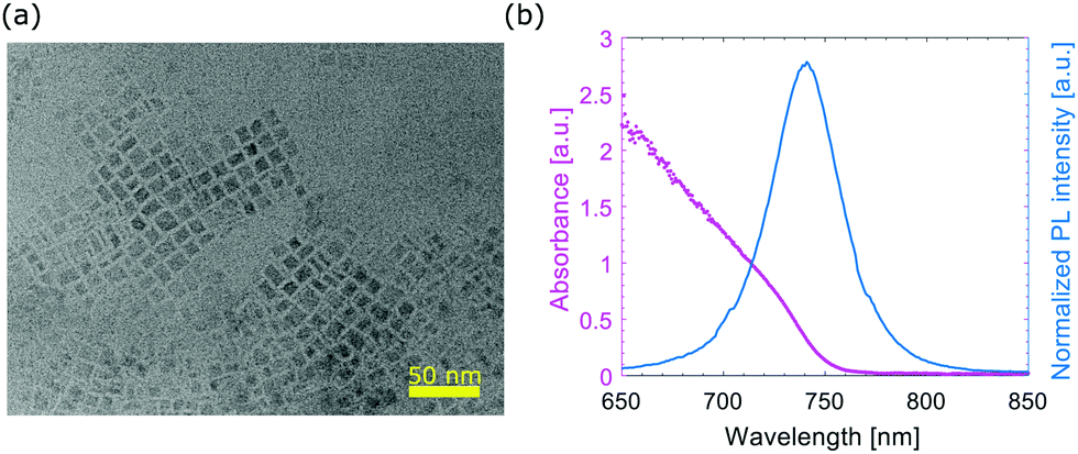 | ||
| Fig. 1 (a) TEM images of C18 capped MAPI NCs; (b) absorbance and photoluminescence of MAPI NCs in toluene. | ||
The band gap of the MAPI NCs was estimated from the photoluminescence (PL) spectrum and the UV-vis absorption spectroscopy, which are both shown in Fig. 1(b). The emission peak and the onset absorption coincide at 745 nm, which corresponds to 1.66 eV.
Three different fabrication methods were investigated to incorporate MAPI NCs in the standard perovskite solar cell architecture, which are shown in Fig. 2. When using method 1 (M1), MAPI NCs were deposited on top of the pre-crystallised perovskite layer and, therefore, introduced just at the perovskite/HTM interface. In contrast, method 2 (M2) used MAPI NCs dispersed in toluene as anti-solvent. It is therefore likely that the NCs partially infiltrated the perovskite layer during crystallisation. Finally, when using method 3 (M3) MAPI NCs were mixed into the MAI solution during conversion of PbI2 into CH3NH3PbI3 and distributed throughout the material. MAPI NCs were also incorporated in inverted perovskite solar cells with NiOx and PCBM used as HTM and ETM respectively. These devices were fabricated using method 1, where MAPI NCs were deposited on top of the crystallised perovskite, as shown in Fig. 2(d).
 | ||
| Fig. 2 Schematic illustration of the three fabrication procedures used for the processing of the perovskite solar cells with C18 capped MAPI NCs; (a) method 1 (M1) with MAPI NCs above the perovskite layer; (b) method 2 (M2) with MAPI NCs embedded in the perovskite layer using an anti-solvent deposition technique; (c) method 3 (M3) with MAPI NCs embedded in the perovskite layer using a 2-step deposition technique; (d) inverted architecture deposited using M1 with MAPI NCs above the perovskite layer at the MAPI/PCBM interface. | ||
MAPI NC are capped by oleic acid (OA) and oleylamine (OLA) surface ligands. It has previously been demonstrated that the COO− functional group in OA and the lone pair on the nitrogen in OLA can coordinate with Pb2+ present at the surface of the MAPI NCs.31–33
Hydrophobic properties
In this work, pure MAPI perovskite material was investigated. Perovskite devices with compositions of mixed cations and mixed halides in the active absorber layer are well known to be much more efficient and stable than pure CH3NH3PbI3.3,34 The purpose of this work was not to make the highest efficiency cells, but to have a reproducible baseline where any changes due to the presence of MAPI NCs could clearly be seen. Therefore, the cells were not optimised for efficiency as it was more important to study the influence of MAPI NCs when incorporated in the standard and inverted architecture. Moreover, we were interested in seeing the effect of MAPI NCs on the stability towards moisture and on the water-resistivity of the surface. Therefore we decided to use the least stable perovskite material, which is pure CH3NH3PbI3.35Fourier transform infrared (FTIR) spectroscopy was used to verify the presence of the C18 capped MAPI NCs in the perovskite films. All FTIR spectra, shown in Fig. S1 in the ESI,† showed N–H and C–H stretching and bending vibrations for MAPI at around 3130, 2800, 1580 and 1470 cm−1, consistent with previous reports in the literature.36 When C18 capped MAPI NCs were incorporated in the perovskite film, an new peak at 2925 cm−1 was observed, which was assigned to stretching of CH2,33 typical of the C18 long chain ligands oleic acid and oleylamine used as surface ligands in the fabrication of MAPI NCs. The peak is particularly visible for films prepared using M1 and M2. The peak intensity is very small compared to the peaks for the bulk MAPI, but confirms the existence of C18 capped MAPI NCs in the materials. The hydrophobic properties of the perovskite films were investigated using contact angle measurements, which are shown in Fig. 3(a). We found that the surface of perovskite films deposited using M1 and M2 were markedly more hydrophobic when the MAPI NCs were incorporated in the architecture. Contact angles higher than 100° were measured. In contrast, films deposited using M3 did not show improvements in the contact angle, indicating that MAPI NCs were not on its surface.
 | ||
| Fig. 3 (a) Contact angle measurements of perovskite films without and with MAPI NCs for perovskite films deposited with methods 1, 2 and 3; from the top to the bottom: 1 – 23° → 101°; 2 – 54° → 92°; 3 – 26° → 26°; (b) picture of perovskite films without and with MAPI NCs deposited on the surface (M1) when one droplet of water is put on the surface; (c) picture of solar cells without (left) and with (right) MAPI NCs after 30 seconds of immersion in water. | ||
The presence of long chain C18 OA + OLA ligands stabilised NCs at the perovskite surface clearly enhanced hydrophobicity. In the fabrication of MAPI NCs, the initial concentration of C18 ligands is 15 vol%. The final product is centrifuged and the solid is re-dispersed in toluene in order to obtain equal volume. The exact amount of C18 ligands present in the final solution of MAPI NCs dispersed in toluene is unknown. However, it is expected to be less than 15 vol%. For comparison, the effect of depositing just the long chain ligands OA on the perovskite layer on the surface contact angle was also examined. This was done to investigate if the ligand alone would impart enhanced stability. A solution with different concentration of OA dispersed in toluene, ranging between 10 and 50 vol%, was deposited onto the perovskite film, using method 1. The contact angle, which is shown in Fig. S2 in the ESI,† increased when the long chain ligands were deposited onto the perovskite layer, reaching a maximum value of 60°. However, even when a solution of 50 vol% of OA in toluene was deposited onto the perovskite film, the surface was less hydrophobic than the one obtained by introducing MAPI NCs in the perovskite layer or on the surface (via M1 and M2).
Fig. 3(b) shows photographs of perovskite films deposited with method 1 without and with MAPI NCs on the surface when some water was dropped onto the surface. The perovskite films with MAPI NCs (on the right hand side) remained dark brown, while, the reference film became quickly yellow. Similar results were observed when the final solar cells were completely immersed in water (Fig. 3(c)). The reference perovskite solar cell (left hand side) underwent a rapid colour change from dark brown to yellow, indicating a complete dissociation of the CH3NH3PbI3 phase into the PbI2 phase, while the cell with integrated MAPI NCs remained dark brown.
XRD patterns of perovskite films with and without MAPI NCs above the perovskite layer are shown in Fig. 4 (films fabricated using M1). After the reference perovskite film was immersed in water for 10 seconds, the PbI2 characteristic peak at 13.2° became the main diffraction peak and the CH3NH3PbI3 phase could no longer be detected. The amount of PbI2 also increased after the perovskite film with MAPI NCs was immersed in water for 10 seconds. However, the tetragonal CH3NH3PbI3 phase was still detected and its characteristic peak at 14.7° was identified as the main diffraction peak, indicating that the tetragonal CH3NH3PbI3 crystalline phase still dominated.
 | ||
| Fig. 4 XRD patterns of films with and without MAPI NCs as soon as deposited and after they have been immersed in water for 10 s. | ||
Photovoltaic performance
Standard and inverted perovskite solar cells with and without MAPI NCs were fabricated using the methods described above. Fig. 5(a) shows the average performing standard mesoporous solar cells fabricated using the three different methods. To examine the reproducibility of photovoltaic performance, different samples were fabricated and measured. Table 1 lists the average values of the main photovoltaic parameters with 95% confidence intervals. The box plots showing the reproducibility of the performance are shown in Fig. S3 in the ESI.† Stabilised power output measurements were collected by monitoring the current when the cell was biased to the maximum power point voltage determined by the JV sweep and are shown in Fig. S5 (ESI†). All devices showed a stable output over 60 s. The PCEs of devices with MAPI NCs incorporated at the interface fabricated using M1 were similar to control cells. While, when methods M2 and M3 were used, the control cells showed a superior performance. JV curves showing both the forward and reverse scans are shown in Fig. S4 in the ESI.† Cells deposited with method M1 showed consistently reduced hysteresis with respect to cells deposited using M2 and M3. The solar cells deposited using the three different methods have similar VOC, which is slightly larger than the VOC measured in control cells. Films fabricated with the anti-solvent technique (M2) show considerably lower photocurrent density and FF, which are reflected in a decreased PCE. The highest performance is obtained by fabricating cells using the first method M1. Cells with larger active area of 0.25 cm2 were also fabricated and shown in Fig. S8 in the ESI.† Devices deposited using method M1 showed PCE of 7.8%. | ||
| Fig. 5 (a) JV curves of average performing solar cells fabricated using the three different deposition method (only the reverse scan is showed, the forward scan is in Fig. S4 in the ESI†); (b) cross-section SEM images of perovskite films without and with C18 capped MAPI NCs. Perovskite solar cells fabricated using the second method M2 via the anti-solvent technique, where the NCs are embedded in the perovskite film; (c) top-view SEM images of perovskite films without and with C18 capped MAPI NCs. Perovskite films deposited using the first method M1, where the NCs are above the perovskite film. | ||
| Param. | Control | M1 | M2 | M3 |
|---|---|---|---|---|
| J SC [mA cm−2] | 19.98 ± 0.26 | 18.48 ± 0.76 | 15.40 ± 1.01 | 18.21 ± 1.08 |
| V OC [V] | 0.73 ± 0.01 | 0.76 ± 0.02 | 0.76 ± 0.01 | 0.76 ± 0.02 |
| FF [—] | 68.57 ± 4.24 | 68.22 ± 1.37 | 61.88 ± 2.99 | 63.54 ± 2.70 |
| PCE [%] | 10.05 ± 0.55 | 9.61 ± 0.32 | 7.19 ± 0.21 | 8.80 ± 0.74 |
The most efficient cell with a mesoporous standard architecture and integrated MAPI NCs was fabricated using method M1 and gave VOC = 0.74 V, JSC = 20.89 mA cm−2, FF = 68.52 and PCE = 10.6%. Cells fabricated using methods M2 and M3, where MAPI NCs are expected to be embedded in the perovskite active layer, showed consistently lower performance. Previous literature data from Cha et al. showed that the introduction of very thin layers of MAPbBrxI3−x QDs on top of CH3NH3PbI3 can change the band edge positions of the material, affecting charge extraction.27 Similar to what we observe here, they found that QDs embedded in the CH3NH3PbI3 perovskite layer produced a PCE of only 6.93%, much lower than what measured when QDs were deposited just at the interface. They attributed the inferior performance to an increased number of recombination centers due to a misalignment of the band edge positions, the hydrophobicity of the films was not investigated.27
In the preparation of MAPI NCs, long chain ligands play a crucial role, preventing the aggregation of the perovskite nanocrystals. However, during the fabrication of quantum dot solar cells, organic ligands are usually removed because they can work as insulating barriers to charge transport between the NCs limiting the PCE of the device.37 Surprisingly, the presence of C18 capped MAPI NCs did not appear to obstruct charge extraction in our standard architecture solar cells.
Photocurrent generation is directly related to the light-harvesting properties of the absorber layer. Gao et al. found that CuInS2 QDs integrated at the perovskite/ETM interface could assist light harvesting, increasing the absorbed light and the device performance.26 To check whether the NCs had an effect on the absorption properties, UV-vis absorption of perovskite films with and without MAPI NCs was measured. The curves, which are shown in Fig. S9 of the ESI,† were found to be very similar, suggesting that the MAPI NCs did not affect light absorption in the active layer. This result is fully consistent with what was previously reported in the literature for perovskite films with MAPbBr3−xIx QDs on top.27
Recently, Yavari et al. observed that the incorporation of carbon nanoparticles into the perovskite active layer could boost the surface coverage of the film by enlarging grains compared to reference perovskite films.38 We investigated possible changes in the morphology through top-view SEM and AFM and cross-sectional SEM images. Fig. 5(b) shows cross section SEM images of perovskite solar cells deposited using method 2 without and with C18 capped MAPI NCs. NCs can not be seen in the active layer and the film thickness does not appear to change. In Fig. 5(c) the surface of perovskite films with and without MAPI NCs deposited on top (M1) is compared through top-view SEM images. These films were deposited by using method 1 to see whether any changes due to the presence of NCs on the surface could clearly be seen. However, changes in the surface morphology are negligible. The influence of the concentration of MAPI NCs on the morphology was also investigated and showed in Fig. S11 in the ESI† through AFM images (films deposited using method 1).
To further investigate the effect that MAPI NCs might have at the interface, different contact layers were used. MAPI NCs were integrated in an inverted structure with NiOx and PCBM used as HTM and ETM respectively by depositing them above the perovskite layer as described in the Experimental section. Fig. 2(d) presents a schematic of the inverted device. Fig. 6(a) shows the JV curves of an inverted solar cell with integrated MAPI NCs measured under forward and reverse scan. Interestingly, inverted hysteresis was observed, where the VOC measured during forward scan was much larger than the one measured during the reverse scan. A similar phenomenon was observed for all the inverted cells with MAPI NCs fabricated for this study. Fig. 6(b) shows the VOC measured by the reverse and forward scan for over 30 different devices fabricated in different days. In contrast, almost no hysteresis was observed in the inverted control devices without MAPI NCs at the CH3NH3PbI3/PCBM interface. A typical JV curve and box plots of the VOC under forward and reverse scan are shown in the ESI† in Fig. S13. The champion control inverted cell without MAPI NCs exhibited VOC = 0.93 V, JSC = 16.74 mA cm−2, FF = 69.71 and PCE = 10.89%, with very low hysteresis. While, very high inverted hysteresis was measured for the solar cells with MAPI NCs. The most efficient cell with an inverted architecture and integrated MAPI NCs exhibited VOC = 0.85 V, JSC = 18.61 mA cm−2, FF = 68.03 and PCE = 10.75% during reverse scan and VOC = 0.95 V, JSC = 17.67 mA cm−2, FF = 43.01 and PCE = 7.18% during forward scan.
 | ||
| Fig. 6 (a) JV curves of an inverted structure perovskite solar cell with MAPI NCs incorporated at the CH3NH3PbI3/ETM interface; (b) comparison of the open circuit voltages measured during forward and reverse scan for over 30 devices. | ||
Recent studies have associated the inverted hysteresis phenomenon with the presence of an extraction barrier at the perovskite/ETM interface.39,40 As suggested by Cha et al., very thin layers of MAPI NCs might change the surface properties of CH3NH3PbI3, affecting the charge extraction.27 Electrochemical experiments can be very useful in understanding the chemical changes occurring at the perovskite/HTM interface.41 The anodic part of CV scans of a perovskite film and a perovskite/MAPI NCs film are shown in Fig. S14(a) in the ESI.† When MAPI NCs were deposited on the surface, the peak slightly shifted to lower voltages. The position of the first oxidation peak of the CH3NH3PbI3 and CH3NH3PbI3/MAPI NCs films was calculated from the onset potential of the redox waves and it was found to be −5.32 eV and −5.27 eV respectively. Very recently, Samu et al. looked at the reduction and oxidation events that occur in halide perovskites and concluded that CV scans alone can not be used to determine the band edge positions of CH3NH3PbI3. Other chemical processes occur in the material within the electrochemical window, therefore the measured currents can not be related to actual carrier injection.42 Even though the exact band edge positions of CH3NH3PbI3 and MAPI NCs can not be determined from CV scans, a consistent difference between the onset potential of the redox events was detected for the studied films, highlighting different material properties. The inverted hysteresis observed in the inverted architecture with MAPI NCs suggested that such interlayer may act as an extraction barrier at the CH3NH3PbI3/ETM interface. When the same NC layer was used at the CH3NH3PbI3/HTM interface no change in the shape of the JV curve was observed suggesting that the NCs are not detrimental at this interface.
Moisture stability
To investigate the stability of the perovskite solar cells, the PCE of two devices with and without C18 capped MAPI NCs was measured 70 days after fabrication. During this time period, the cells were left in an ambient atmosphere without encapsulation, in the dark, at open circuit with relative humidity (RH) measured to be 60 ± 10% (also known as shelf-stability). Two sets of cells were fabricated on the same day and exposed to the same ageing process. Two solar cells with similar initial PCEs were evaluated, the JV curves measured on the day of fabrication and after 70 days are shown in Fig. 7. The PCE of the reference cell decreased by over 40%. The main parameter affecting the reduced PCE was the current density. This might be due to a degradation of the perovskite CH3NH3PbI3 to PbI2, due to the presence of moisture which caused a decreased light harvesting. In contrast, the cell with integrated MAPI NCs decreased by only 10%, showing what we believe to be enhanced stability towards moisture due to the hydrophobic nature of CH3NH3PbI3/MAPI NCs layers.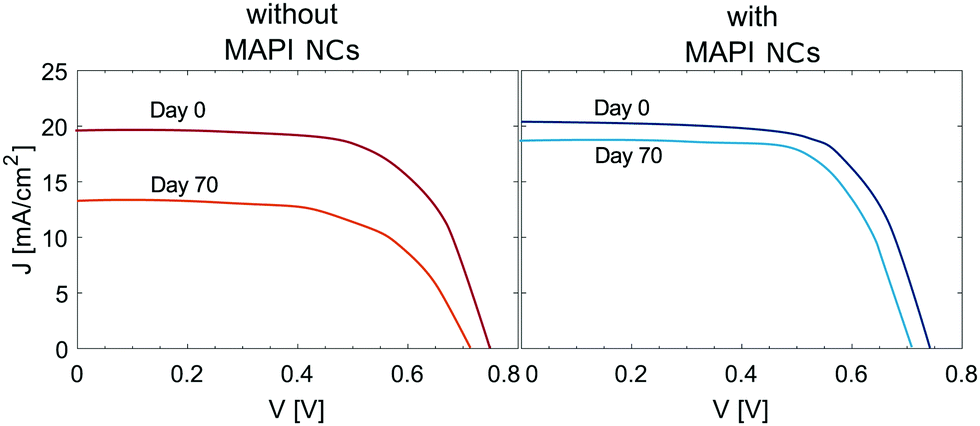 | ||
| Fig. 7 Shelf-stability of the perovskite devices fabricated using method 1. JV curves of solar cells without and with MAPI NCs as soon as fabricated and after 70 days of ageing in ambient atmosphere (method 1 M1 was used to fabricate these cells). Without MAPI NCs – day 0: PCE = 9.57%, day 70: PCE = 5.81%; with MAPI NCs – day 0: PCE = 10.47%, day 70: PCE = 9.27%. | ||
Conclusions
We developed standard mesoporous and inverted perovskite solar cells with integrated C18 capped MAPI NCs. Inverted hysteresis was observed in the inverted architecture, suggesting that the MAPI NCs introduced an extraction barrier at the CH3NH3PbI3/ETM interface. In contrast, the hole extraction was not affected when the MAPI NCs were deposited at the CH3NH3PbI3/HTM interface in standard mesoporous cells.Three different deposition methods were investigated. MAPI NCs were deposited just at the CH3NH3PbI3/HTM interface and embedded in the perovskite active layer. When using method 1, in which MAPI NCs were above the perovskite layer, solar cells with PCEs over 10% were measured. While, when using method 2 with MAPI NCs embedded in the perovskite layer, devices with only 7% conversion efficiency were obtained.
MAPI NCs did not contribute to the light-harvesting, however they gave the perovskite films higher hydrophobicity with surface water contact angles that exceeded 100°. XRD measurements showed that the tetragonal CH3NH3PbI3 phase was retained after the film was immersed in water for 10 s. Such hydrophobic properties allowed solar cells with MAPI NCs to be much more stable towards moisture with respect to the reference perovskite solar cells.
MAPI NCs were fabricated in a flow reactor, in ambient conditions and at room temperature, therefore, no complex production steps were added to the PSC fabrication. Flow chemistry allows fast reactions, clean products and it is a technique that is very easy to scale-up, which is crucial for viable and commercial photovoltaic technologies.
Conflicts of interest
There are no conflicts to declare.Acknowledgements
We acknowledge the MAS staff at University of Bath for their assistance in SEM acquisition. We would like to thank the EPSRC Centre for Doctoral Training in Sustainable Chemical Technologies (EP/L016354/1). This project has received funding from the European Union's Horizon 2020 research and innovation programme H2020-MSCA-CO-FUND-2014 (# 665992, MSCA FIRE: Fellows with Industrial Research Enhancement).References
- M. A. Green, A. Ho-Baillie and H. J. Snaith, Nat. Photonics, 2014, 8, 506–514 CrossRef.
- M. M. Lee, J. Teuscher, T. Miyasaka, T. N. Murakami and H. J. Snaith, Science, 2012, 338, 643–647 CrossRef PubMed.
- W. S. Yang, B.-W. Park, E. H. Jung, N. J. Jeon, Y. C. Kim, D. U. Lee, S. S. Shin, J. Seo, E. K. Kim, J. H. Noh and S. I. Seok, Science, 2017, 356, 1376–1379 CrossRef PubMed.
- G. A. Nemnes, C. Besleaga, V. Stancu, D. E. Dogaru, L. N. Leonat, L. Pintilie, K. Torfason, M. Ilkov, A. Manolescu and I. Pintilie, J. Phys. Chem. C, 2017, 121, 11207–11214 CrossRef.
- N. K. Noel, S. D. Stranks, A. Abate, C. Wehrenfennig, S. Guarnera, A.-A. Haghighirad, A. Sadhanala, G. E. Eperon, S. K. Pathak, M. B. Johnston, A. Petrozza, L. M. Herz and H. J. Snaith, Energy Environ. Sci., 2014, 7, 3061 RSC.
- F. Hao, C. C. Stoumpos, D. H. Cao, R. P. Chang and M. G. Kanatzidis, Nat. Photonics, 2014, 8, 489–494 CrossRef.
- C. Liu, J. Fan, H. Li, C. Zhang and Y. Mai, Sci. Rep., 2016, 6, 35705 CrossRef PubMed.
- F. Giustino and H. J. Snaith, ACS Energy Lett., 2016, 1, 1233–1240 CrossRef.
- D. Wang, M. Wright, N. K. Elumalai and A. Uddin, Sol. Energy Mater. Sol. Cells, 2016, 147, 255–275 CrossRef.
- N. Aristidou, C. Eames, I. Sanchez-molina, X. Bu, J. Kosco, M. S. Islam and S. A. Haque, Nat. Commun., 2017, 8, 1–40 CrossRef PubMed.
- A. M. A. Leguy, Y. Hu, M. Campoy-Quiles, M. I. Alonso, O. J. Weber, P. Azarhoosh, M. van Schilfgaarde, M. T. Weller, T. Bein, J. Nelson, P. Docampo and P. R. F. Barnes, Chem. Mater., 2015, 27, 3397–3407 CrossRef.
- S. Yang, Y. Wang, P. Liu, Y.-B. Cheng, H. J. Zhao and H. G. Yang, Nat. Energy, 2016, 1, 1–7 Search PubMed.
- I. Poli, S. Eslava and P. Cameron, J. Mater. Chem. A, 2017, 5, 22325–22333 RSC.
- B. Li, C. Fei, K. Zheng, X. Qu, T. Pullerits, G. Cao and J. Tian, J. Mater. Chem. A, 2016, 4, 17018–17024 RSC.
- Q. Wang, Q. Dong, T. Li, A. Gruverman and J. Huang, Adv. Mater., 2016, 28, 6734–6739 CrossRef PubMed.
- J. Idigoras, F. J. Aparicio, L. Contreras-Bernal, S. Ramos-Terrón, M. Alcaire, J. R. Sanchez-Valencia, A. Borras, A. Barranco and J. A. Anta, ACS Appl. Mater. Interfaces, 2018, 10, 11587–11594 CrossRef PubMed.
- A. Palma, L. Cinà, S. Pescetelli, A. Agresti, M. Raggio, R. Paolesse, F. Bonaccorso and A. Di Carlo, Nano Energy, 2016, 22, 349–360 CrossRef.
- C. Ma, C. Leng, Y. Ji, X. Wei, K. Sun, L. Tang, J. Yang, W. Luo, C. Li, Y. Deng, S. Feng, J. Shen, S. Lu, C. Du and H. Shi, Nanoscale, 2016, 338, 643–647 Search PubMed.
- H. Tsai, W. Nie, J.-C. Blancon, C. C. Stoumpos, R. Asadpour, B. Harutyunyan, A. J. Neukirch, R. Verduzco, J. J. Crochet, S. Tretiak, L. Pedesseau, J. Even, M. A. Alam, G. Gupta, J. Lou, P. M. Ajayan, M. J. Bedzyk, M. G. Kanatzidis and A. D. Mohite, Nature, 2016, 536, 312–316 CrossRef PubMed.
- D. H. Cao, C. C. Stoumpos, T. Yokoyama, J. L. Logsdon, T.-B. Song, O. K. Farha, M. R. Wasielewski, J. T. Hupp and M. G. Kanatzidis, ACS Energy Lett., 2017, 2, 982–990 CrossRef.
- I. C. Smith, E. T. Hoke, D. Solis-Ibarra, M. D. McGehee and H. I. Karunadasa, Angew. Chem., Int. Ed., 2014, 53, 11232–11235 CrossRef PubMed.
- G. Grancini, I. Zimmermann, E. Mosconi, D. Martineau and S. Narbey, Nat. Commun., 2017, 8, 1–8 CrossRef PubMed.
- D. A. Jacobs, Y. Wu, H. Shen, C. Barugkin, F. J. Beck, T. P. White, K. Weber and K. R. Catchpole, Phys. Chem. Chem. Phys., 2017, 19, 3094–3103 RSC.
- S. V. Reenen, M. Kemerink and H. J. Snaith, J. Phys. Lett., 2015, 6, 3808–3814 Search PubMed.
- W. Deng, X. Liang, P. S. Kubiak and P. J. Cameron, Adv. Energy Mater., 2018, 8, 1–20 Search PubMed.
- F. Gao, H. Dai, H. Pan, Y. Chen, J. Wang and Z. Chen, J. Colloid Interface Sci., 2017, 513, 693–699 CrossRef PubMed.
- M. Cha, P. Da, J. Wang, W. Wang, Z. Chen, F. Xiu, G. Zheng and Z.-S. Wang, J. Am. Chem. Soc., 2016, 138, 8581–8587 CrossRef PubMed.
- T. Y. Wen, S. Yang, P. F. Liu, L. J. Tang, H. W. Qiao, X. Chen, X. H. Yang, Y. Hou and H. G. Yang, Adv. Energy Mater., 2018, 1703143, 1–7 Search PubMed.
- A. Capasso, F. Matteocci, L. Najafi, M. Prato, J. Buha, L. Ciná, V. Pellegrini, A. D. Carlo and F. Bonaccorso, Adv. Energy Mater., 2016, 6, 1–12 Search PubMed.
- X. Liang, W. Deng, K. Wu, R. Baker, D. Ferdani, L. Torrente-Murciano and P. Cameron, 2018, submitted.
- A. Pan, B. He, X. Fan, Z. Liu, J. J. Urban, A. P. Alivisatos, L. He and Y. Liu, ACS Nano, 2016, 10, 7943–7954 CrossRef PubMed.
- S. Sun, D. Yuan, Y. Xu, A. Wang and Z. Deng, ACS Nano, 2016, 10, 3648–3657 CrossRef PubMed.
- Y. Zhao, X. Xu and X. You, Sci. Rep., 2016, 6, 1–8 CrossRef PubMed.
- A. D. Jodlowski, C. Roldán-Carmona, G. Grancini, M. Salado, M. Ralaiarisoa, S. Ahmad, N. Koch, L. Camacho, G. De Miguel and M. K. Nazeeruddin, Nat. Energy, 2017, 2, 972–979 CrossRef.
- T. Leijtens, K. Bush, R. Cheacharoen, R. Beal, A. Bowring and M. D. McGehee, J. Mater. Chem. A, 2017, 5, 11483–11500 RSC.
- Y. Wang, T. Mahmoudi, W. Y. Rho, H. Y. Yang, S. Seo, K. S. Bhat, R. Ahmad and Y. B. Hahn, Nano Energy, 2017, 40, 408–417 CrossRef.
- J. Peng, Y. Chen, X. Zhang, A. Dong and Z. Liang, Adv. Sci., 2016, 3, 1500432 CrossRef PubMed.
- M. Yavari, M. Mazloum-Ardakani, S. Gholipour, N. Marinova, J. L. Delgado, S.-H. Turren-Cruz, K. Domanski, N. Taghavinia, M. Saliba, M. Grätzel, A. Hagfeldt and W. Tress, Adv. Energy Mater., 2018, 8, 1702719 CrossRef.
- W. Tress, J. P. Correa Baena, M. Saliba, A. Abate and M. Graetzel, Adv. Energy Mater., 2016, 6, 1–11 Search PubMed.
- H. Shen, D. A. Jacobs, Y. Wu, T. Duong, J. Peng, X. Wen, X. Fu, S. K. Karuturi, T. P. White, K. Weber and K. R. Catchpole, J. Phys. Chem. Lett., 2017, 8, 2672–2680 CrossRef PubMed.
- L. Zhao, R. A. Kerner, Z. Xiao, Y. L. Lin, K. M. Lee, J. Schwartz and B. P. Rand, ACS Energy Lett., 2016, 1, 595–602 CrossRef.
- G. F. Samu, R. A. Scheidt, P. V. Kamat and C. Janáky, Chem. Mater., 2018, 30, 561–569 CrossRef PubMed.
Footnote |
| † Electronic supplementary information (ESI) available. See DOI: 10.1039/c8tc01939h |
| This journal is © The Royal Society of Chemistry 2018 |