
 Open Access Article
 This Open Access Article is licensed under a
 Creative Commons Attribution 3.0 Unported Licence
Efficient perovskite light-emitting diodes based on a solution-processed tin dioxide electron transport layer†
Heyong
Wang
a,
Hongling
Yu
a,
Weidong
Xu
 a,
Zhongcheng
Yuan
a,
Zhibo
Yan
ab,
Chuanfei
Wang
a,
Xianjie
Liu
a,
Mats
Fahlman
a,
Jun-Ming
Liu
b,
Xiao-Ke
Liu
*acd and
Feng
Gao
*a
a,
Zhongcheng
Yuan
a,
Zhibo
Yan
ab,
Chuanfei
Wang
a,
Xianjie
Liu
a,
Mats
Fahlman
a,
Jun-Ming
Liu
b,
Xiao-Ke
Liu
*acd and
Feng
Gao
*a
aDepartment of Physics, Chemistry and Biology (IFM), Linköping University, Linköping 58183, Sweden. E-mail: xiaoke.liu@liu.se; feng.gao@liu.se
bLaboratory of Solid State Microstructures, Innovation Center of Advanced Microstructures, Nanjing University, Nanjing 210093, P. R. China
cState Key Laboratory of Luminescent Materials and Devices, South China University of Technology, Guangzhou 510640, P. R. China
dState Key Lab of Silicon Materials, Zhejiang University, Hangzhou 310027, P. R. China
First published on 6th June 2018
Abstract
To achieve high-performance perovskite light-emitting diodes (PeLEDs), an appropriate functional layer beneath the perovskite emissive layer is significantly important to modulate the morphology of the perovskite film and to facilitate charge injection and transport in the device. Herein, for the first time, we report efficient n–i–p structured PeLEDs using solution-processed SnO2 as an electron transport layer. Three-dimensional perovskites, such as CH(NH2)2PbI3 and CH3NH3PbI3, are found to be more chemically compatible with SnO2 than with commonly used ZnO. In addition, SnO2 shows good transparency, excellent morphology and suitable energy levels. These properties make SnO2 a promising candidate in both three- and low-dimensional PeLEDs, among which a high external quantum efficiency of 7.9% has been realized. Furthermore, interfacial materials that are widely used to improve the device performances of ZnO-based PeLEDs are also applied on SnO2-based PeLEDs and their effects have been systematically studied. In contrast to ZnO, SnO2 modified by these interfacial materials shows detrimental effects due to photoluminescence quenching.
Introduction
Metal halide perovskites have attracted enormous attention in recent years as promising semiconducting materials in optoelectronic applications, such as solar cells, light-emitting diodes (LEDs), lasers, transistors and photodetectors.1–5 These materials show exceptional properties such as suitable bandgaps, high absorption coefficients, low trap densities, and long carrier diffusion lengths, leading to rapid progress in solar cells, among which a high power conversion efficiency (PCE) over 22% has been achieved.6,7 Furthermore, they also exhibit outstanding light-emitting properties, such as high colour purity, readily tuneable emissions and high photoluminescence quantum yields (PLQYs), making them promising candidates for displays and lighting applications.8,9 Within the last four years, increasing efforts have been devoted to developing efficient perovskite LEDs (PeLEDs).10–17To realize high-efficiency PeLEDs, charge transport layers, including hole transport layers (HTLs) and electron transport layers (ETLs), are employed to balance hole- and electron-injection and transport.18 In general, there are two types of device architectures for PeLEDs, p–i–n and n–i–p, which refer to a layer preparation sequence in the form of a p-type layer, an intrinsic layer and an n-type layer and the reverse sequence, respectively. For efficient p–i–n based PeLEDs, vacuum-deposited organic molecules, such as 2,2′,2′′-(1,3,5-benzenetriyl)-tris(1-phenyl-1-H-benzimidazole) (TPBi) and 2,9-dimethyl-4,7-diphenyl-1,10-phenanthroline (BCP), are employed as the ETLs.10,19 In contrast, efficient n–i–p based PeLEDs are fabricated through all solution processes, where colloidal zinc oxide (ZnO) nanoparticles are usually used as the ETLs.11,20–24 Despite high efficiencies in PeLEDs, ZnO could cause the problem of chemical instability in the perovskite films,25,26 limiting its applications in PeLEDs. Therefore, it is desired to develop new types of solution-processed ETLs for efficient n–i–p based PeLEDs.
Solution-processed inorganic metal oxides, such as titanium dioxide (TiO2) and tin dioxide (SnO2), are potential ETL candidates for efficient PeLEDs. These materials have large bandgaps, a suitable conduction band minimum (CBM) for electron injection and a deep valence band maximum (VBM) for hole blocking.27–29 In addition, their thin films show good transparency in the visible-infrared region of 400–900 nm, minimizing optical energy losses caused by the ETL.30,31 Efforts have been made to develop PeLEDs using solution-processed TiO2, which however show a relatively low external quantum efficiency (EQE) of 0.48%.14 Moreover, preparation of the TiO2 layer requires high-temperature (>450 °C) sintering, which is a barrier for low-cost and stretchable PeLEDs. In addition to TiO2, solution-processed SnO2 has also been widely used as the ETL in organic, dye-sensitized, and perovskite solar cells.28–33 Furthermore, SnO2 has high mobilities (∼240 cm2 V−1 s−1 and 1.9 × 10⁻³ cm2 V−1 s−1 for bulk and nanoparticle films, respectively) and a high electrical conductivity (1.82 × 10⁻⁸ S cm−1 at room temperature).34,35 For instance, You and co-workers reported hysteresis-free perovskite solar cells with PCEs of around 20% based on colloidal SnO2 nanoparticles.34 Given that the SnO2 film has suitable energy levels, good transparency and high electron mobility, it is thus natural to expect that the use of the solution-processed SnO2 ETL would be a fruitful approach for obtaining high-efficiency solution-processed PeLEDs.
Herein, for the first time, we report efficient n–i–p structured PeLEDs using solution-processed SnO2 as the ETL. It is found that three-dimensional (3D) perovskites, such as CH(NH2)2PbI3 (FAPbI3) and CH3NH3PbI3 (MAPbI3), show considerably enhanced chemical compatibility with SnO2 compared with ZnO. More importantly, both 3D- and low-dimensional perovskite based PeLEDs using SnO2 as the ETL exhibit high efficiencies, among which a high EQE of 7.9% has been realized. These results suggest that SnO2 can be used as an efficient ETL in solution-processed PeLEDs. Furthermore, interfacial materials, such as polyethylenimine ethoxylated (PEIE) and polyethylenimine (PEI), that have been widely used to improve the device performances of ZnO-based PeLEDs are also employed in SnO2-based PeLEDs, the effects of which have been systematically studied. Unexpectedly, these two interfacial materials show detrimental effects on SnO2 based PeLEDs due to photoluminescence quenching.
Results and discussion
The morphology of the SnO2 film obtained by spin-coating colloidal SnO2 nanoparticles on an ITO-coated glass substrate is investigated by using atomic force microscopy (AFM). As shown in Fig. 1a, a smooth and pinhole-free SnO2 film with a root-mean-square (RMS) roughness of 1.24 nm is obtained. Fig. 1b shows the transmission spectra of the SnO2 and ZnO films prepared on ITO-coated glass substrates, respectively. The SnO2 film exhibits similar transparency to the ZnO film between 420 and 850 nm. Note that the SnO2 film shows excellent transparency with transmission values greater than 97% in the ultraviolet-visible-infrared region, suggesting that the SnO2 layer will cause minimized optical energy losses in PeLEDs with a wide range of emissive wavelengths. In particular, in the ultraviolet region below 400 nm, where the ZnO film starts to absorb light (the bandgap of ZnO is ∼3.53 eV),36 the SnO2 film still shows good transparency with transmission values greater than 95% due to a much larger bandgap of ∼3.74 eV,34 showing promise as a good ETL candidate for ultraviolet LEDs.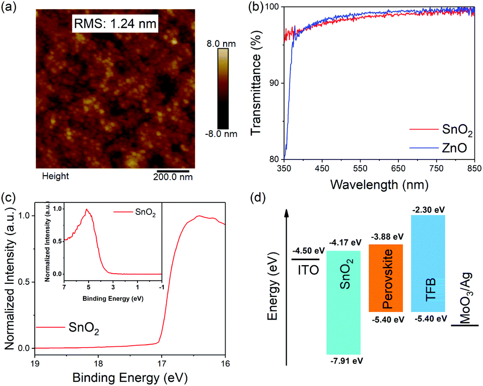 | ||
| Fig. 1 (a) AFM height image of the SnO2 film. (b) Transmission spectra of the SnO2 and ZnO films deposited on ITO-coated glass substrates, respectively. (c) UPS cutoff edge of the SnO2 film, inset: valence band edge. (d) Flat-band energy-level diagram of the materials used in this study. | ||
The electronic states and band structures of the SnO2 film and a low-dimensional perovskite film consisting of FAPbI3: 60 mol% NMAI (NMAI = C10H7CH2NH2·HI) are studied by ultraviolet photoelectron spectroscopy (UPS). The work functions (WFs) of the SnO2 and perovskite films are calculated to be −4.17 eV and −4.18 eV, respectively (Fig. 1c and Fig. S1a, ESI†). The CBM and VBM of the perovskite film calculated from the UPS spectra and Tauc plot (Fig. S1b, ESI†) are −3.88 eV and −5.40 eV, respectively. As shown in Fig. 1d, the CBM of the SnO2 layer matches well with that of the perovskite layer, facilitating efficient electron injection from the ETL into the perovskite emissive layer; the valence band maximum of the SnO2 layer (−7.91 eV) is much deeper than that of the perovskite layer, offering efficient hole blocking. Therefore, the SnO2 film exhibits smooth morphology, excellent transparency and suitable energy levels, which is promising as an ETL candidate for PeLEDs.
We use a one-step spin-coating method to form 3D perovskite films (FAPbI3 and MAPbI3) on the SnO2 and ZnO films with various annealing temperatures to study their chemical compatibility with the underlying SnO2 and ZnO, respectively. The crystal structures of these films are investigated by X-ray diffraction (XRD). As shown in Fig. 2a, the FAPbI3 films deposited on SnO2 show a dominant diffraction peak at 11.8° when they are annealed below 120 °C, which can be assigned to the (010) lattice plane of the yellow phase.37,38 Interestingly, a diffraction peak at 13.9° that belongs to the (111) lattice plane of the black phase can be observed when annealed at 120 °C, accompanied by the colour change of the perovskite films (Fig. 2a). When they are annealed above 120 °C, the FAPbI3 films start to decompose into lead iodide (PbI2), the (001) lattice plane of which is located at 12.6°. However, it is worth noting that the FAPbI3 film shows a pure black phase when annealed at 160 °C for 1 min although decomposition starts at longer annealing times (Fig. S2, ESI†). In comparison, the FAPbI3 films deposited on ZnO start to decompose into PbI2 when the annealing temperature is higher than 120 °C, below which the films are in the yellow phase. The colour of the films is an obvious indication showing the change of the phases (Fig. 2c). Similarly, the MAPbI3 films deposited on ZnO starts to decompose into PbI2 when annealed at 80 °C, and the diffraction peak of MAPbI3 is hardly observed when annealed at 90 °C and 100 °C, accompanied by an obvious colour change of the films (Fig. 2d). It is impressive that the MAPbI3 films deposited on SnO2 are stable below 100 °C; no obvious colour change of the perovskite films is observed at a high annealing temperature up to 160 °C (Fig. 2b). These results demonstrate that the 3D perovskite films show considerably enhanced chemical compatibility with SnO2 compared with ZnO, suggesting feasible applications of SnO2 in PeLEDs where perovskite films require a wide range of annealing temperatures.
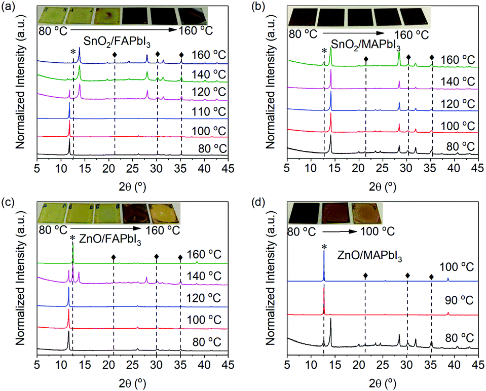 | ||
| Fig. 2 XRD patterns and photographs of 3D perovskite films deposited on the SnO2 and ZnO films with various annealing temperatures. (a) FAPbI3 films deposited on SnO2, (b) MAPbI3 films deposited on SnO2. (c) FAPbI3 films deposited on ZnO. (d) MAPbI3 films deposited on ZnO. * represents the diffraction peak of PbI2, ♦ represents the diffraction peak of ITO. | ||
We further study the morphologies and optoelectronic properties of the FAPbI3 film (annealed at 120 °C) deposited on SnO2. As shown in Fig. 3a and b, the film shows smooth (RMS: 9.3 nm) and pinhole-free morphologies with large grains. The absorption and PL spectra of the FAPbI3 film deposited on SnO2 were also measured and are shown in Fig. S3 (ESI†). The absorption onset is located at 813 nm, corresponding to an energy bandgap of 1.52 eV. In addition, this film shows narrow emission peaked at 811 nm with a PLQY of 7%. A PeLED is fabricated with the structure of indium tin oxide (ITO)/SnO2 (30 nm)/FAPbI3 (480 nm)/poly(9,9-dioctyl-fluorene-co-N-(4-butylphenyl)diphenylamine) (TFB, 40 nm)/MoO3 (7 nm)/Ag (80 nm). As shown in Fig. 3c, the device has a very low turn-on voltage (the driving voltage when emission is detectable) of 1.2 V and a maximum radiance of 26 W sr−1 m−2. It is interesting to note that the turn-on voltage (Von) of this device is quite lower than the theoretical limit of 1.52 V according to the bandgap (Eg) of FAPbI3 (Vtheoreticalon = Eg/e, where e is the unit charge), which may be explained by an Auger-assisted energy upconversion model.39–41 Since TFB has a hole mobility of ∼1.0 × 10⁻² cm2 V−1 s−1 which is an order of magnitude higher than that of the electron mobility of the SnO2 nanoparticle film, there is a negligible hole injection barrier between the perovskite layer and TFB.42 Thus, holes and electrons are likely to accumulate at the interface between SnO2 and the perovskite layer. With electrons accumulating at the interface, an Auger-assisted electron injection process can take place, in which one high-energy electron can be generated after absorbing the energy released from the interfacial recombination of an electron–hole pair. The resulting high-energy electron can overcome the injection barrier between the perovskite layer and SnO2 and recombine with the hole inside the perovskite EML to emit a photon. In addition, this device exhibits a very low EQE at low current density which increases to a moderate maximum value of 0.9% at a high current density of ∼400 mA cm−2. This finding can be explained by the low exciton binding energy of the large-grain FAPbI3 crystals, where non-radiative trap-assisted recombination is dominant at low carrier excitation densities and radiative bimolecular recombination gradually increases with increasing excitation density.43
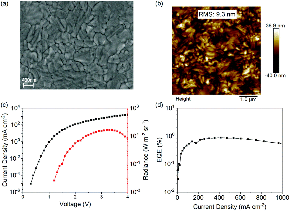 | ||
| Fig. 3 (a) SEM image and (b) AFM image of the FAPbI3 film deposited on SnO2. (c) Current density–voltage–radiance and (d) EQE–current density curves of the device based on FAPbI3 deposited on SnO2. | ||
In order to investigate the generality of the SnO2 ETL in PeLEDs, we further investigated low-dimensional perovskites prepared on SnO2. Low-dimensional perovskites can be synthesized by incorporating bulky organic ammonium cations that are too large to fit into the interspace between the PbX64− (X = I, Br, and Cl) octahedral layers and therefore split large perovskite grains into different types of nanocrystals.20,43,44 In this study, we prepare a series of low-dimensional perovskites by adjusting the molar ratios between 1-naphthylmethylammonium iodide (NMAI) and FAPbI3, expressed as FAPbI3: x mol% NMAI (x = 20, 40, 60, 80, and 100). These films are formed by one-step spin-coating from precursor solutions on SnO2, followed by thermal annealing at 100 °C. XRD measurements are conducted to determine the composition and crystallinity of the perovskite films. As mentioned above, the FAPbI3 film annealed at 100 °C is in the yellow phase (Fig. 2a), whereas the addition of NMAI lowers the transition temperature of the black phase (Fig. 4a). With 20 mol% NMAI, most of the perovskites have been transferred into the black phase. With further increasing ratios of NMAI, the diffraction peaks assigned to layered perovskites are observed, indicating that the as-formed films are composed of grains distinct from the 3D perovskites. The average crystal sizes of the low-dimensional perovskite films are calculated from the XRD results by using the Debye–Scherrer equation (eqn (S1), ESI†). As shown in Table S1 (ESI†), the addition of NMAI gradually decreases the average crystal size from 28.3 nm (3D FAPbI3) to 16.2 nm (x = 0.8). The top-view scanning electron microscopy (SEM) image of FAPbI3: 60 mol% NMAI clearly shows the formation of tiny grains (Fig. 4b). AFM measurements are also performed to investigate the morphology of this film. As shown in Fig. S4 (ESI†), the film consists of small grains and exhibits a RMS of 16.6 nm.
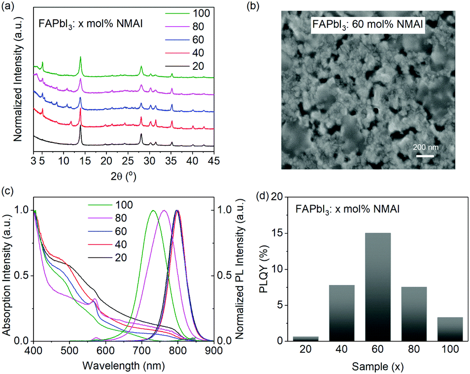 | ||
| Fig. 4 (a) XRD patterns, (b) top-view SEM image, (c) absorption and PL spectra, and (d) PLQYs of FAPbI3: x mol% NMAI (x = 20, 40, 60, 80, and 100) films prepared on SnO2. | ||
The normalized absorption and PL spectra of these low-dimensional perovskite films are shown in Fig. 4c. The addition of 20 and 40 mol% NMAI to FAPbI3 slightly changes the absorption and PL spectra, whereas more amounts of NMAI induce the formation of the 〈n = 2〉-layered perovskite, in which the characteristic absorption peak is located at 573 nm.20,44,45 The PL spectra, peaked at 798 nm with a full width at half maximum (FWHM) of 54 nm, almost remain the same when the NMAI contents are below 60 mol%. It is also interesting to note that obvious blue-shifted PL spectra are observed when 80 and 100 mol% NMAI are introduced (PL spectra peaked at 762 nm and 732 nm, respectively), which may be caused by the size-dependent quantum confinement effect.46 In addition, the FWHM of these two spectra are broadened to 89 nm (x = 80) and 81 nm (x = 100), respectively. The wider PL spectra may be originated from several low-dimensional emissive components – as indirect evidence of a clear PL peak at 573 nm that derives from the 〈n = 2〉 -layered perovskite can be observed. The PLQYs of these films change along with the ratios of NMAI, among which the addition of 60 mol% NMAI contributes to the highest PLQY of 15% (Fig. 4d).
PeLEDs are fabricated to investigate the electroluminescent (EL) properties of these low-dimensional perovskites with SnO2 as the ETL. The device structure is the same as that of the FAPbI3-based PeLED except the emitting layer. The current density–voltage–radiance curves of these PeLEDs are shown in Fig. 5a. It should be noted that the addition of NMAI gradually decreases the current densities of the devices due to the insulating nature of NMAI. In addition, the FAPbI3: 80 mol% NMAI and FAPbI3: 100 mol% NMAI-based devices show gradually increased turn-on voltages compared with those with lower amounts of NMAI. This can be explained by their relatively wider bandgaps. The EQE–voltage curves of these devices are shown in Fig. 5b, among which the FAPbI3: 60 mol% NMAI based device shows the highest EQE of 7.9%. The statistical external quantum efficiency from 44 devices presents an average EQE of 6.8% (Fig. S5, ESI†). The results demonstrate that SnO2 is a good ETL for PeLEDs based on low-dimensional perovskites in addition to 3D perovskites. Fig. 5c shows the normalized EL spectra of these devices which exhibit a similar shift tendency to the PL spectra.
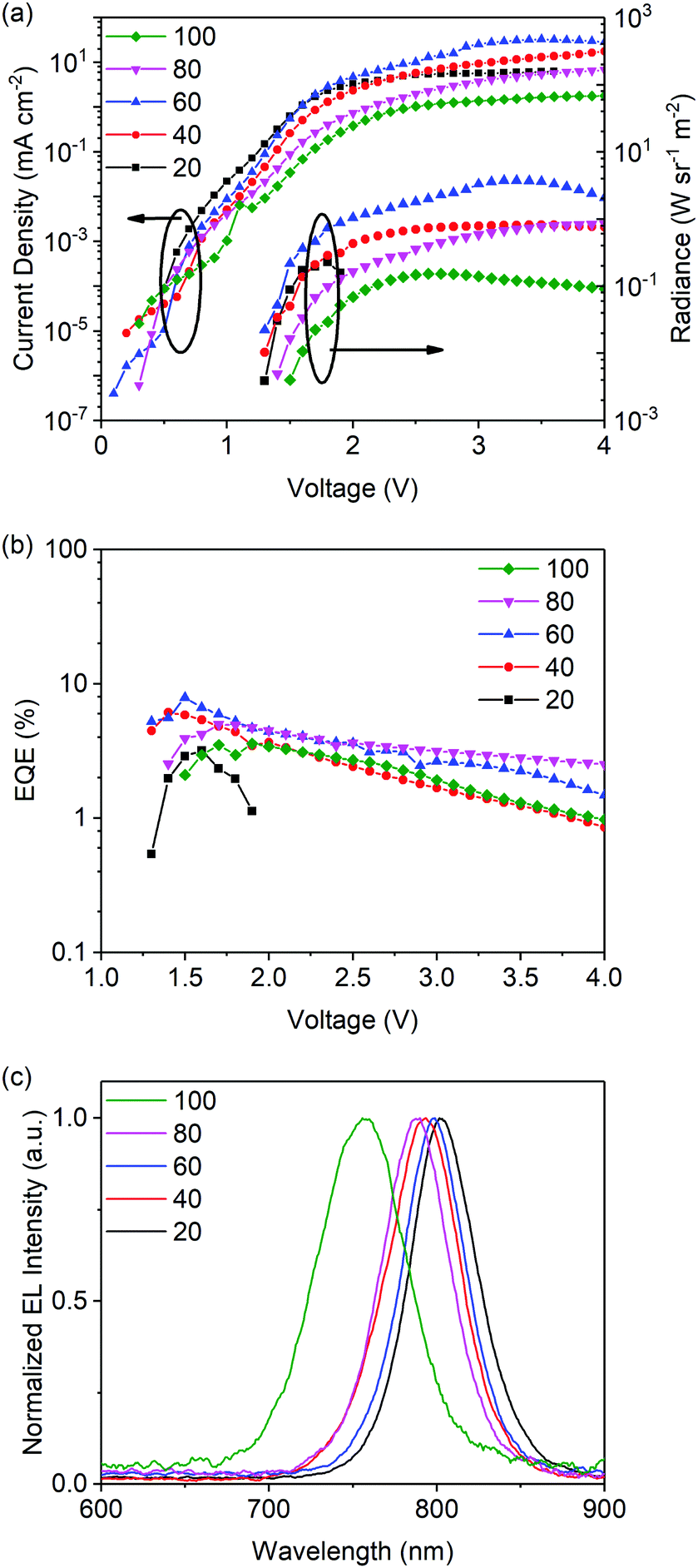 | ||
| Fig. 5 (a) Current density–voltage–radiance curves, (b) EQE–voltage curves, and (c) EL spectra of low-dimensional PeLEDs with FAPbI3: x mol% NMAI (x = 20, 40, 60, 80, and 100) films as the EMLs and SnO2 as the ETLs. | ||
It is reported that interfacial materials, such as PEIE and PEI, can modify the ETL surface and show favourable effects on the device performances.11,20 For instance, Wang et al. reported that 3D perovskites show a better morphology of PEI-modified ZnO, and consequently deliver higher device performances.11 In addition, these interfacial materials are able to tailor the work function of the contacts and can be used to control electron injection.47 Therefore, it is desired to study their effects on SnO2 based PeLEDs. Fig. 6a shows the XRD patterns of the FAPbI3: 60 mol% NMAI films prepared on SnO2, SnO2/PEI and SnO2/PEIE substrates, respectively. These films show similar XRD patterns, suggesting that these two interfacial materials have a negligible impact on the perovskite crystal structure. The CBM of the PEIE-modified SnO2 film is changed from −4.17 eV to −3.73 eV due to the shift of the WF (Fig. S6, ESI†). The more matching energy level with the perovskite layer (−3.88 eV) facilitates easier electron extraction from the perovskite layer.48 Although these perovskite films show similar PL spectra (Fig. 6b), the perovskite films prepared on SnO2/PEI and SnO2/PEIE exhibit gradually reduced PLQYs, indicating PL quenching caused by these interfacial materials. The transient PL decay characteristics of these perovskite films were investigated and are shown in Fig. 6c. The transient PL decay spectra are fitted with a bi-exponential decay function consisting of two time constants, suggesting a fast decay pathway and a slow decay pathway in these films. The fast decay pathway is associated with the quenching of free carriers in the perovskite domains caused by the substrate layers. As shown in Table S2 (ESI†), the fraction of the short decay time constants declines in the film with PEIE (or PEI). In consideration of the thick perovskite film (∼480 nm, shown in Fig. S7, ESI†), the slow decay pathway can be assigned to the PL decay of the residual free carriers that are far from the interfacial layer.
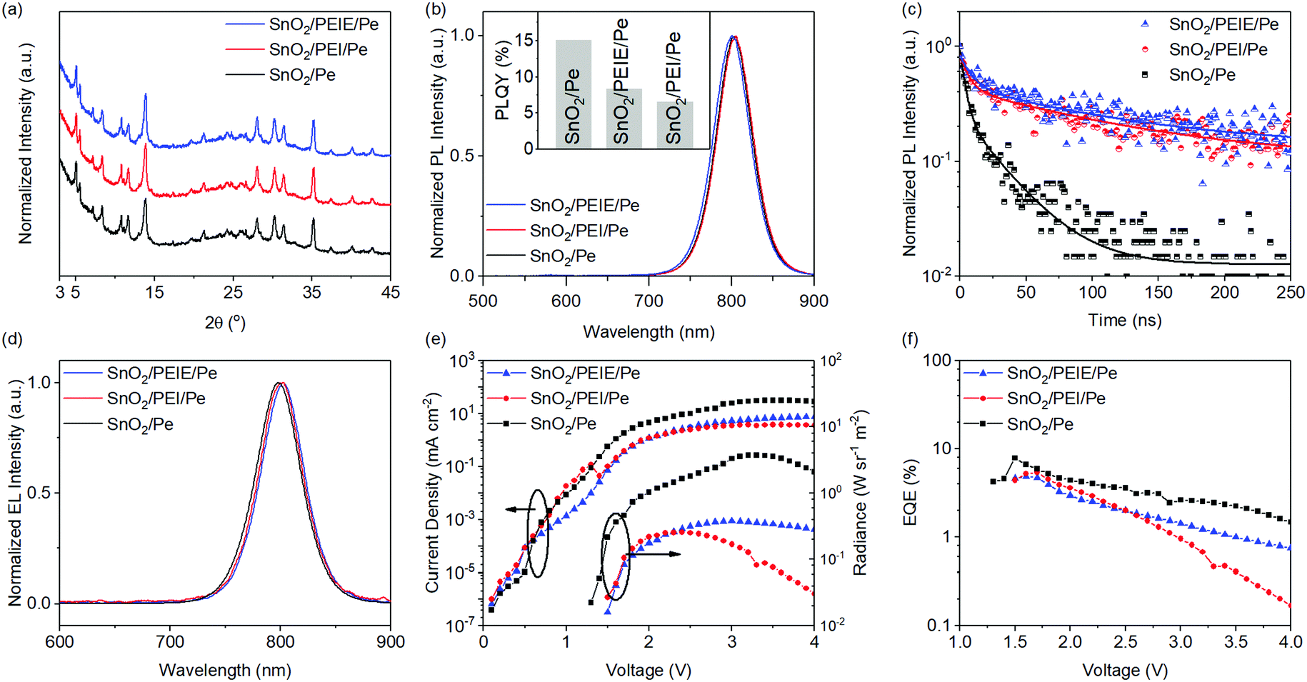 | ||
| Fig. 6 (a) XRD patterns, (b) PL spectra, (c) PL decay curves of the FAPbI3: 60 mol% NMAI films prepared on SnO2, SnO2/PEI, and SnO2/PEIE, respectively. (d) Normalized EL spectra, (e) current density–voltage–radiance curves and (f) EQE–voltage curves of the FAPbI3: 60 mol% NMAI based PeLED devices with SnO2, SnO2/PEI, and SnO2/PEIE as the ETLs. | ||
The interfacial materials are then employed in PeLED devices, the performance efficiencies of which are shown in Fig. 6d–f. Compared with the device without an interfacial layer, the device using PEIE (or PEI) shows reduced current densities and higher turn-on voltages, which may be due to the insulating nature of these materials. Unlike those based on ZnO, the device with PEIE (or PEI) modified SnO2 exhibits detrimental effects on the device performances.11,15 The PeLEDs with PEIE and PEI deliver EQEs of 4.9% and 5.4%, respectively, lower than that (7.9%) of the device without the interfacial layer. The results are in line with the PL measurements and confirm that the interfacial materials (PEIE and PEI) show detrimental effects due to increased non-radiative recombination. This observation may be useful for perovskite solar cells where charge extraction is found to be favourable.
Conclusions
In conclusion, for the first time, we have systematically studied the effects of solution-processed SnO2 as the ETL in n–i–p structured PeLEDs based on both three- and low-dimensional perovskites. SnO2 exhibits a smooth morphology, suitable energy levels, good electron-transporting properties and excellent transparency with transmission values greater than 95% in ultraviolet–visible–infrared regions. In addition, the 3D perovskites (FAPbI3 and MAPbI3) show considerably enhanced chemical compatibility with SnO2 compared with ZnO. A series of PeLEDs are fabricated using SnO2 as the ETL, among which a high EQE of 7.9% is realized, demonstrating that SnO2 can be a good solution-processed ETL for n–i–p structured PeLEDs. Furthermore, interfacial studies suggest that the interfacial materials (PEI and PEIE) facilitate charge extraction in the SnO2 based perovskite films and consequently cause PL quenching and lower efficiencies.Conflicts of interest
There are no conflicts to declare.Acknowledgements
This work is supported by the ERC Starting Grant (717026), the Carl Tryggers Stiftelse, the China Scholarship Council, the European Commission Marie Skłodowska-Curie Actions (691210), CeNano and the Swedish Government Strategic Research Area in Materials Science on Functional Materials at Linköping University (Faculty Grant SFO-Mat-LiU no. 2009-00971). Z. Y. thanks the VINNMER and Marie Skłodowska-Curie Fellowship provided by Vinnova. X. K. Liu is a VINNMER and Marie Skłodowska-Curie Fellow (No. 2016-02051), and would like to thank financial support from the State Key Laboratory of Luminescent Materials and Devices at South China University of Technology (No. 2017-skllmd-05) and the State Key Lab of Silicon Materials at Zhejiang University (No. SKL2017-03).References
- Z.-K. Tan, R. S. Moghaddam, M. L. Lai, P. Docampo, R. Higler, F. Deschler, M. Price, A. Sadhanala, L. M. Pazos, D. Credgington, F. Hanusch, T. Bein, H. J. Snaith and R. H. Friend, Nat. Nanotechnol., 2014, 9, 687 CrossRef PubMed.
- A. Swarnkar, A. R. Marshall, E. M. Sanehira, B. D. Chernomordik, D. T. Moore, J. A. Christians, T. Chakrabarti and J. M. Luther, Science, 2016, 354, 92 CrossRef PubMed.
- G. Xing, N. Mathews, S. S. Lim, N. Yantara, X. Liu, D. Sabba, M. Grätzel, S. Mhaisalkar and T. C. Sum, Nat. Mater., 2014, 13, 476 CrossRef PubMed.
- C. R. Kagan, Science, 1999, 286, 945 CrossRef PubMed.
- L. Dou, Y. M. Yang, J. You, Z. Hong, W. H. Chang, G. Li and Y. Yang, Nat. Commun., 2014, 5, 5404 CrossRef PubMed.
- NREL, Efficiency Chart, https://www.nrel.gov/pv/assets/images/efficiency-chart.png, vol. 10, 2017, accessed.
- W. S. Yang, B. Park, E. H. Jung and N. J. Jeon, Science, 2017, 356, 1376 CrossRef PubMed.
- Y. H. Kim, H. Cho, J. H. Heo, T. S. Kim, N. S. Myoung, C. L. Lee, S. H. Im and T. W. Lee, Adv. Mater., 2015, 27, 1248 CrossRef PubMed.
- Y. Bekenstein, B. A. Koscher, S. W. Eaton, P. Yang and A. P. Alivisatos, J. Am. Chem. Soc., 2015, 137, 16008 CrossRef PubMed.
- H. Cho, S. H. Jeong, M. H. Park, Y. H. Kim, C. Wolf, C. L. Lee, J. H. Heo, A. Sadhanala, N. S. Myoung, S. Yoo, S. H. Im, R. H. Friend and T. W. Lee, Science, 2015, 350, 1222 CrossRef PubMed.
- J. Wang, N. Wang, Y. Jin, J. Si, Z. K. Tan, H. Du, L. Cheng, X. Dai, S. Bai, H. He, Z. Ye, M. L. Lai, R. H. Friend and W. Huang, Adv. Mater., 2015, 27, 2311 CrossRef PubMed.
- L. Protesescu, S. Yakunin, M. I. Bodnarchuk, F. Krieg, R. Caputo, C. H. Hendon, R. X. Yang, A. Walsh and M. V. Kovalenko, Nano Lett., 2015, 15, 3692 CrossRef PubMed.
- X. Zhang, H. Lin, H. Huang, C. Reckmeier, Y. Zhang, W. C. H. Choy and A. L. Rogach, Nano Lett., 2016, 16, 1415 CrossRef PubMed.
- O. A. Jaramillo-Quintero, R. S. Sanchez, M. Rincon and I. Mora-Sero, J. Phys. Chem. Lett., 2015, 6, 1883 CrossRef PubMed.
- G. Li, F. W. R. Rivarola, N. J. L. K. Davis, S. Bai, T. C. Jellicoe, F. De La Peña, S. Hou, C. Ducati, F. Gao, R. H. Friend, N. C. Greenham and Z. K. Tan, Adv. Mater., 2016, 28, 3528 CrossRef PubMed.
- X. Yang, X. Zhang, J. Deng, Z. Chu, Q. Jiang, J. Meng, P. Wang, L. Zhang, Z. Yin and J. You, Nat. Commun., 2018, 9, 570 CrossRef PubMed.
- J. Si, Y. Liu, Z. He, H. Du, K. Du, D. Chen, J. Li, M. Xu, H. Tian, H. He, D. Di, C. Lin, Y. Cheng, J. Wang and Y. Jin, ACS Nano, 2017, 11, 11100 CrossRef PubMed.
- S. A. Veldhuis, P. P. Boix, N. Yantara, M. Li, T. C. Sum, N. Mathews and S. G. Mhaisalkar, Adv. Mater., 2016, 28, 6804 CrossRef PubMed.
- Y. Ling, Z. Yuan, Y. Tian, X. Wang, J. C. Wang, Y. Xin, K. Hanson, B. Ma and H. Gao, Adv. Mater., 2016, 28, 305 CrossRef PubMed.
- N. Wang, L. Cheng, R. Ge, S. Zhang, Y. Miao, W. Zou, C. Yi, Y. Sun, Y. Cao, R. Yang, Y. Wei, Q. Guo, Y. Ke, M. Yu, Y. Jin, Y. Liu, Q. Ding, D. Di, L. Yang, G. Xing, H. Tian, C. Jin, F. Gao, R. H. Friend, J. Wang and W. Huang, Nat. Photonics, 2016, 10, 699 CrossRef.
- J. Duan, Q. Xiong, H. Wang, J. Zhang and J. Hu, J. Mater. Sci.: Mater. Electron., 2017, 28, 60 CrossRef.
- Z.-F. Shi, X.-G. Sun, D. Wu, T.-T. Xu, S.-W. Zhuang, Y.-T. Tian, X.-J. Li and G.-T. Du, Nanoscale, 2016, 8, 10035 RSC.
- X. Liang, S. Bai, X. Wang, X. Dai, F. Gao, B. Sun, Z. Ning, Z. Ye and Y. Jin, Chem. Soc. Rev., 2017, 46, 1730 RSC.
- Y.-Z. Zheng, E.-F. Zhao, F.-L. Meng, X.-S. Lai, X.-M. Dong, J.-J. Wu and X. Tao, J. Mater. Chem. A, 2017, 5, 12416 RSC.
- G. Yang, H. Tao, P. Qin, W. Ke and G. Fang, J. Mater. Chem. A, 2016, 4, 3970 RSC.
- J. Yang, B. D. Siempelkamp, E. Mosconi, F. De Angelis and T. L. Kelly, Chem. Mater., 2015, 27, 4229 CrossRef.
- B. Bob, T. Bin Song, C. C. Chen, Z. Xu and Y. Yang, Chem. Mater., 2013, 25, 4725 CrossRef.
- W. Q. Wu, F. Huang, D. Chen, Y. B. Cheng and R. A. Caruso, Adv. Funct. Mater., 2015, 25, 3264 CrossRef.
- H. J. Snaith and C. Ducati, Nano Lett., 2010, 10, 1259 CrossRef PubMed.
- F. Gu, S. F. Wang, M. K. Lü, G. J. Zhou, D. Xu and D. R. Yuan, J. Phys. Chem. B, 2004, 108, 8119 CrossRef.
- P. Tao, Y. Li, A. Rungta, A. Viswanath, J. Gao, B. C. Benicewicz, R. W. Siegel and L. S. Schadler, J. Mater. Chem., 2011, 21, 18623 RSC.
- Q. Dong, Y. Shi, K. Wang, Y. Li, S. Wang, H. Zhang, Y. Xing, Y. Du, X. Bai and T. Ma, J. Phys. Chem. C, 2015, 119, 10212 CrossRef.
- J. Song, E. Zheng, J. Bian, X.-F. Wang, W. Tian, Y. Sanehira and T. Miyasaka, J. Mater. Chem. A, 2015, 3, 10837 RSC.
- Q. Jiang, L. Zhang, H. Wang, X. Yang, J. Meng, H. Liu, Z. Yin, J. Wu, X. Zhang and J. You, Nat. Energy, 2016, 2, 16177 CrossRef.
- F. Yakuphanoglu, J. Alloys Compd., 2009, 470, 55 CrossRef.
- K. Qasim, B. Wang, Y. Zhang, P. Li, Y. Wang, S. Li, S. T. Lee, L. S. Liao, W. Lei and Q. Bao, Adv. Funct. Mater., 2017, 27, 1606874 CrossRef.
- C. C. Stoumpos, C. D. Malliakas and M. G. Kanatzidis, Inorg. Chem., 2013, 52, 9019 CrossRef PubMed.
- Q. Han, S. H. Bae, P. Sun, Y. T. Hsieh, Y. Yang, Y. S. Rim, H. Zhao, Q. Chen, W. Shi, G. Li and Y. Yeng, Adv. Mater., 2016, 28, 2253 CrossRef PubMed.
- L. Qian, Y. Zheng, J. Xue and P. H. Holloway, Nat. Photonics, 2011, 5, 543 CrossRef.
- A. K. Pandey and J. M. Nunzi, Adv. Mater., 2007, 19, 3613 CrossRef.
- H. Shen, W. Cao, N. T. Shewmon, C. Yang, L. S. Li and J. Xue, Nano Lett., 2015, 15, 1211 CrossRef PubMed.
- H. H. Fong, A. Papadimitratos and G. G. Malliaras, Appl. Phys. Lett., 2006, 89, 172116 CrossRef.
- M. Yuan, L. N. Quan, R. Comin, G. Walters, R. Sabatini, O. Voznyy, S. Hoogland, Y. Zhao, E. M. Beauregard, P. Kanjanaboos, Z. Lu, D. H. Kim and E. H. Sargent, Nat. Nanotechnol., 2016, 11, 872 CrossRef PubMed.
- Z. Xiao, R. A. Kerner, L. Zhao, N. L. Tran, K. M. Lee, T. W. Koh, G. D. Scholes and B. P. Rand, Nat. Photonics, 2017, 11, 108 CrossRef.
- Z. Chen, C. Zhang, X. F. Jiang, M. Liu, R. Xia, T. Shi, D. Chen, Q. Xue, Y. J. Zhao, S. Su, H. L. Yip and Y. Cao, Adv. Mater., 2017, 8, 29 Search PubMed.
- J. A. Sichert, Y. Tong, N. Mutz, M. Vollmer, S. Fischer, K. Z. Milowska, R. García Cortadella, B. Nickel, C. Cardenas-Daw, J. K. Stolarczyk, A. S. Urban and J. Feldmann, Nano Lett., 2015, 15, 6521 CrossRef PubMed.
- Y. Zhou, C. Fuentes-Hernandez, J. Shim, J. Meyer, A. J. Giordano, H. Li, P. Winget, T. Papadopoulos, H. Cheun, J. Kim, M. Fenoll, A. Dindar, W. Haske, E. Najafabadi, T. M. Khan, H. Sojoudi, S. Barlow, S. Graham, J. L. Brédas, S. R. Marder, A. Kahn and B. Kippelen, Science, 2012, 336, 327 CrossRef PubMed.
- H. Zhou, Q. Chen, G. Li, S. Luo, T.-b. Song, H.-S. Duan, Z. Hong, J. You, Y. Liu and Y. Yang, Science, 2014, 345, 542 CrossRef PubMed.
Footnote |
| † Electronic supplementary information (ESI) available. See DOI: 10.1039/c8tc01871e |
| This journal is © The Royal Society of Chemistry 2018 |