Ultrathin film heterojunctions by combining solution processing and sublimation for ambipolar organic field-effect transistors†
Received
30th March 2018
, Accepted 29th June 2018
First published on 2nd July 2018
Abstract
Ambipolar organic field-effect transistors based on binary blends of n- and p-type semiconductors frequently suffer from low or unbalanced electron and hole transport. Uncontrolled phase separation and intermixing of donor and acceptor phases in such thin film blends lead to formation of bulk heterojunctions that lack sufficient percolation paths to ensure effective transport of free charge carriers of both signs. In this work, we present a novel approach to improve the functionality of ambipolar transistors based on a common conjugated polymer, namely poly(3-hexylthiophene) (P3HT), and a small molecular naphthalene derivative (NDI-C9). We studied the correlation between the morphology and the performance of P3HT and NDI-C9 blend transistors with bulk, bilayer and structured bulk-like heterostructures. The bulk heterostructure was obtained from solution, while the bilayer and ordered bulk-like morphologies were produced by a combination of solution and vacuum deposition. The best ambipolar performance with balanced electron and hole transport was found for the bulk-like heterojunction structures of NDI-C9 evaporated onto the P3HT fiber network spin-cast from a pre-aggregated toluene solution.
Introduction
Organic electronics have been drawing considerable attention from science and industry in recent decades,1,2 mainly due to promising potential applications of organic semiconductors in large scale and low cost photovoltaic devices,3 displays,4 or elastic circuits.5 Despite a lot of effort put into the development of organic semiconductors and devices, some important issues still need to be studied and solved to meet the expectations of practical applications.6,7 Since almost all digital circuits contain n- and p-type transistors with symmetric characteristics, strong focus is put on the development of ambipolar, organic field-effect transistors (OFETs). Such devices would allow the construction of efficient photodetectors8 or complementary transistor pairs employing the same semiconducting films capable of transporting either holes or electrons, depending on the electric potential applied to the gate electrode.9 Due to the fact that n-type organic semiconductors are sensitive to ambient conditions9 and suffer from electron trapping,10,11 fabrication of stable and efficient ambipolar OFETs remains a challenging task.12 One of the promising approaches to form ambipolar devices involves the usage of two different organic semiconductors – one showing high electron conductivity and the other one capable of efficient hole transport. In this case, ambipolar films can be realized as bulk heterojunctions consisting of both semiconductors,13,14 or as bilayer structures with electron and hole transporting layers deposited on top of each other.15,16
In this work, we present a novel way to fabricate ambipolar OFETs utilizing a prominent hole transporting polymer, i.e. poly(3-hexylthiophene) (P3HT), and an electron transporting low molecular weight naphthalene derivative (NDI-C9) via a combination of solution processing and thermal evaporation. The impact of the morphology of the bulk and bilayer heterojunction structure on the device performance is discussed. Ambipolar OFETs with symmetric hole and electron transport (μh and μe ∼ 10−2 cm2 V−1 s−1) are based on ultrathin, aggregated P3HT nanofiber networks spin-cast from aged toluene solution and covered with thermally evaporated NDI-C9 layers. The ultrathin semiconducting films, i.e. thinner than 10 nm, hold great potential for applications in elastic and transparent devices due to their beneficial mechanical and optical properties.17 Since the majority of the charge transport takes place near the semiconductor/dielectric interface, it is possible to correlate the charge transport properties and the heterojunction morphology of the films. Knowledge of such a correlation would bring general understanding of the device characteristics of ambipolar transistors.18,19 For this reason, special attention has been paid to monitor and analyze the building-up of the NDI-C9 layer on the ultrathin P3HT nanofiber network.
Experimental
Materials
P3HT with Mw = 94.1 kg mol−1, polydispersity index PDI = 1.90 and regioregularity (RR) = 95.5 was purchased from Ossila. Solvents (HPLC grade) were purchased from Sigma-Aldrich. All compounds and solvents were used as received.
Synthesis of NDI-C9
The synthetic route to N,N′-dinonyl-1,4,5,8-naphthalenedicarboximide (NDI-C9) used in this study (Scheme 1) followed the procedure known for perylene diimides.20,21 Imidazole (1.6 g, 24 mmol), 1,4,5,8-naphthalenetetracarboxylic dianhydride (0.8 g, 3 mmol) and n-nonylamine (1.0 g, 7 mmol) were suspended in toluene (20 mL) and stirred at 150–155 °C for about 12 h. After cooling to room temperature, toluene was removed under vacuum. The obtained residue was then dispersed in ethanol (96%, ∼30 mL). The resulting suspension was added in portions to cold 2 N hydrochloric acid (∼60 mL) and stirred for about one hour. The precipitation was filtered off, and washed with water (3 × 25 mL) and methanol (4 × 10 mL). The crude product was placed in a thimble and extracted with methanol in a Soxhlet apparatus for about 8 h. Afterwards, the remaining solid was extracted with chloroform and the extraction was continued for approx. 3 h. During this time, all solute in chloroform was transferred to the flask. The chloroform solution of the product was evaporated to dryness. The residue was treated with methanol (25 mL) and filtered off to give 1.2 g (78%) of N,N′-dinonyl-1,4,5,8-naphthalenedicarboximide (NDI-C9). The chemical structure of obtained NDI-C9 was confirmed by 1H and 13C NMR spectroscopy. 1H NMR (600 MHz, CDCl3) δ: 0.87 (t, 6H, J = 7.0 Hz, CH3), 1.21–1.32 (m, 16H, CH3(![[C with combining low line]](https://www.rsc.org/images/entities/char_0043_0332.gif)
![[H with combining low line]](https://www.rsc.org/images/entities/char_0048_0332.gif)
![[2 with combining low line]](https://www.rsc.org/images/entities/char_0032_0332.gif) )
)![[4 with combining low line]](https://www.rsc.org/images/entities/char_0034_0332.gif) ), 1.36 (quint, 4H, J = 7.5 Hz, (CH2)3N), 1.43 (quint, 4H, J = 7.4 Hz, (CH2)2N), 1.74 (quint, 4H, J = 7.7 Hz, CH2N), 4.19 (t, 4H, J = 7.7 Hz, CH2N), 8.75 (s, 4H, ArH); 13C NMR (150 MHz, CDCl3) δ: 14.11, 22.67, 27.10, 28.09, 29.26, 29.34, 29.49, 31.86, 41.00, 126.60, 126.64, 130.89, 162.78. 1H and 13C NMR spectra are in good agreement with literature data.22
), 1.36 (quint, 4H, J = 7.5 Hz, (CH2)3N), 1.43 (quint, 4H, J = 7.4 Hz, (CH2)2N), 1.74 (quint, 4H, J = 7.7 Hz, CH2N), 4.19 (t, 4H, J = 7.7 Hz, CH2N), 8.75 (s, 4H, ArH); 13C NMR (150 MHz, CDCl3) δ: 14.11, 22.67, 27.10, 28.09, 29.26, 29.34, 29.49, 31.86, 41.00, 126.60, 126.64, 130.89, 162.78. 1H and 13C NMR spectra are in good agreement with literature data.22
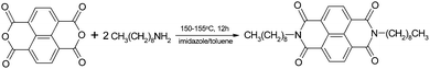 |
| | Scheme 1 Reaction scheme of N,N′-dinonyl-1,4,5,8-naphthalenedicarboximide (NDI-C9). | |
Preparation and measurements of OFETs
All devices were prepared on silicon substrates with a 300 nm silicon-dioxide layer (Ossila). Before the deposition of the active semiconducting film, the substrates were washed in acetone and isopropanol in an ultrasonic bath. Each washing cycle lasted 15 min. Then, the substrates were UV-irradiated in an oxygen atmosphere for 50 min. Afterwards, HMDS vapor treatment of the substrates was performed at 140 °C for 6 h. After the cleansing and HMDS modification, the substrates were transferred to the glove-box system with an inner nitrogen atmosphere. For the bulk heterojunction structure, solutions of P3HT:NDI-C9 blends were prepared by dissolving both P3HT and NDI-C9 in toluene in three different concentration ratios: the P3HT![[thin space (1/6-em)]](https://www.rsc.org/images/entities/char_2009.gif) :NDI-C9 1:1 blend contained 2.5 mg of polymer and 2.5 mg of the small molecule dissolved in 1 mL of toluene; the P3HT:NDI-C9 1:3 blend contained 2.5 mg of polymer and 7.5 mg of the small molecule dissolved in 1 mL of toluene; the P3HT:NDI-C9 1:15 blend contained 0.7 mg of polymer and 10.5 mg of the small molecule dissolved in 1 mL of toluene. Solutions were stirred and heated at 80 °C for complete dissolution. Active films were spin-cast with a 3000 rpm spinning speed for 3 min. The prepared films were annealed in vacuum at 80 °C for 4 h.
:NDI-C9 1:1 blend contained 2.5 mg of polymer and 2.5 mg of the small molecule dissolved in 1 mL of toluene; the P3HT:NDI-C9 1:3 blend contained 2.5 mg of polymer and 7.5 mg of the small molecule dissolved in 1 mL of toluene; the P3HT:NDI-C9 1:15 blend contained 0.7 mg of polymer and 10.5 mg of the small molecule dissolved in 1 mL of toluene. Solutions were stirred and heated at 80 °C for complete dissolution. Active films were spin-cast with a 3000 rpm spinning speed for 3 min. The prepared films were annealed in vacuum at 80 °C for 4 h.
Films with an ordered bulk-like morphology were prepared by a combination of a solution approach and thermal evaporation. Firstly, P3HT solutions were prepared by dissolving the polymer in toluene (concentration = 2 mg mL−1 or 5 mg mL−1 for thick films for GIWAXS measurements) and stirred at 80 °C for complete dissolution. Pristine (non-aggregated) P3HT films were spin-cast from a hot solution at 8000 rpm for the thinnest layers to 800 rpm for the thickest layers, while aggregated P3HT fibrils were fabricated by means of spin-coating under the same conditions from toluene solution cooled down to 25 °C and stored at that temperature for 24 h. Subsequently, the films were removed from the glove-box, transferred into the vacuum-deposition system and annealed at 80 °C for 4 h under high vacuum of 0.5 × 10⁻⁶ mPa. Then, at the same temperature of the substrate the NDI-C9 layer was evaporated on the top of P3HT at a deposition rate of 0.2 Å s−1. Afterwards, the films were kept for 12 h in vacuum for cooling down to room temperature.
Gold source and drain electrodes were thermally evaporated to a nominal thickness (the value indicated by the quartz balance) of 60 nm through a shadow mask. As a result, OFETs in the bottom gate, top contact configuration with a 1 mm channel width and a 15 to 30 μm channel length were produced. The device characterization was performed under a nitrogen atmosphere, using a Keithley 2634B source meter connected to a needle-probe station. Mobilities were calculated from the transfer characteristics in the saturation regime in the higher Vds voltage regime (from −80 V to −60 V for p-type and from 60 V to 80 V for n-type, measured with a 250 ms rate), using the following formula:
where
μ stands for the charge carrier mobility,
Id is the drain current,
W the channel width,
L the channel length,
Ci the capacitance of gate dielectric,
Vg the gate voltage and
Vth the threshold voltage. Average charge carrier mobilities are obtained for 5–6 devices, while their error margins were calculated as the sample standard deviations.
Atomic force microscopy (AFM)
A Veeco Dimension 3100 atomic force microscope was used to investigate the microstructure and to determine the thickness of the blend films. All images were obtained in tapping mode with Olympus silicon cantilevers at a 320 kHz resonance frequency. The film thickness was determined by the NanoScope Analysis software from height profiles of the topography images for the scratched films that represent the average cross sections. Examples for the thickness analysis from step-height profiles are presented in Fig. S1 (ESI†). Each presented value is an average derived from eight measurements of different areas of the samples. The uncertainty was estimated as the standard deviation of the mean value.
Time of flight secondary ion mass spectrometry (TOF-SIMS)
The secondary ion mass spectra were recorded using a TOF-SIMS IV mass spectrometer manufactured by IONTOF GmbH, Muenster, Germany. The instrument is equipped with a Bi liquid metal ion gun and a high mass resolution time of flight mass analyzer. Secondary ion mass spectra were recorded from the area of about 100 × 100 μm2 under irradiation with pulses of 25 keV Bi3+ ions at a repetition rate of 10 kHz and an average ion current of 0.4 pA. The acquisition time was 30 s giving an ion dose below the static limit of 1 × 10¹² ions per cm2.
NDI-C9 HOMO and LUMO level determination
Building 3D models of molecules, DFT calculations and analysis were performed using Materials Studio 8 (Biovia) and the DMol3 module. For the calculations, the B3LYP hybrid functional and the Tkatchenko-Scheffler dispersion correction were used. All calculations were carried out on non-periodic systems (a single, isolated molecule). The DFT calculations were performed in two steps: (i) geometry optimization, and (ii) a single-point energy calculation. The geometry optimization convergence thresholds for the energy change, the maximum force, and the maximum displacement between optimization steps were set to 1 × 10⁻⁵ Ha, 0.002 Ha Å−1 and 0.005 Å, respectively.
Grazing-incidence wide-angle x-ray scattering (GIWAXS)
GIWAXS measurements were performed by means of a solid anode X-ray tube (a Siemens Kristalloflex X-ray source, and a copper anode X-ray tube operated at 30 kV and 20 mA), Osmic confocal MaxFlux optics, an X-ray beam with pinhole collimation and a MAR345 image plate detector. The beam size was 1.0 mm × 0.2 mm (width × height), and samples were irradiated just below the critical angle for total reflection with respect to the incoming X-ray beam (∼0.12°). The scattering intensity was detected on a 2-D image plate (MAR-345) with a pixel size of 150 μm (2300 × 2300 pixels). The raw detector image needs to be converted into reciprocal-space. This was done by using a calibration standard (silver behenate). All X-ray scattering measurements were performed under vacuum (∼1 mbar) to reduce air scattering and beam damage to the sample. All GIWAXS data processing and analysis were performed by using the software package Datasqueeze (http://www.datasqueezesoftware.com).
Results and discussion
Bulk heterojunction structure of solution processed films
Simplicity is an important feature when it comes to fabrication of ambipolar OFETs. Therefore, solution-based processing is beneficial especially in the case of one-step film deposition.23–25 For this reason, in the first step ambipolar OFETs based on bulk heterojunction films of NDI-C9 and P3HT were obtained solely by solution processing. The blend was prepared by dissolution of both compounds in toluene. The solution was spin-cast on HMDS treated Si/SiO2 wafers to form the P3HT:NDI-C9 binary blend films. However, the solution-based approach did not provide satisfying results in terms of efficient ambipolar OFETs. Blends with P3HT:NDI-C9 concentration ratios of 1:1 and 1:3 showed no, or weak electron transport, respectively (Fig. S1a and b, ESI†). Balanced hole and electron transport with mobilities around 1.5 × 10⁻³ cm2 V−1 s−1 was achieved for a ratio of 1:15 P3HT:NDI-C9 (Fig. S1c, ESI†). Lower ratios formed a bilayer type morphology which frequently occurs when compounds with stronger molecule-to-molecule than molecule-to-substrate interactions tend to separate at the upper layer of the blend film, while the compound which preferentially absorbs to the substrate forms the bottom layer.26–28 However, in our work, the NDI-C9 molecules assembled into ca. 0.8 μm small domains with many grain boundaries and discontinuities between each other (Fig. S2a, ESI†), hindering the electron transport. The 1:15 blend exhibited a bulk heterojunction morphology of disordered and randomly distributed NDI-C9 domains, which was the cause of the rather low mobility of these films (Fig. S2b, ESI†). The bulk heterojunction films exhibited a thickness above 50 nm, which is significantly thicker than the desired ultrathin regime. Solutions with a similar ratio but lower concentrations exhibited much worse film forming properties (due to dwetting) and therefore thinner films could not be achieved. To enhance the performance of the P3HT:NDI-C9 based transistors, a different approach for the film deposition was employed.
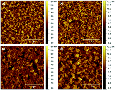
Bilayer film structure
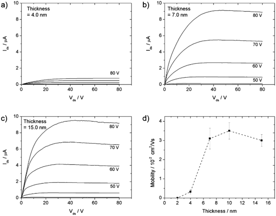
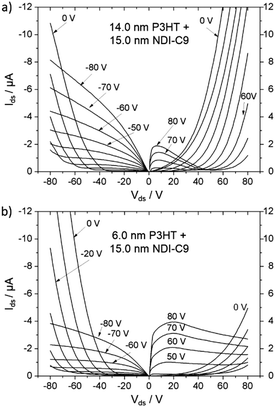
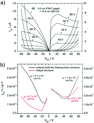
An ambipolar transistor can be also be composed of a bilayer structure with electron and hole transporting layers fabricated on top of each other. In such OFETs, the conducting pathway for one type of carriers is created near the dielectric interface, while charges of opposite sign are transported near the heterojunction interface.15,29 The solution processing of bilayers requires the application of orthogonal solvents to avoid the dissolution of the bottom film during the deposition of the top one leading typically to a poor interface quality. This requirement limits the choice of organic semiconductors since most of them show similar solubility in organic solvents.13,30 An alternative approach towards fabrication of bilayer structures is the combination of solution processing of the bottom layer and thermal evaporation of the top layer.31,32 This methodology was adopted in the case of P3HT/NDI-C9 planar bilayer heterojunctions. In order to optimize processing of the bilayer devices, first pristine NDI-C9 films were thermally evaporated in a thickness range from 2.0 nm to 20.0 nm on Si/SiO2 HMDS-treated substrates and the microstructure and electrical properties of the produced layers were investigated. Fig. 1 shows the microstructure of evaporated NDI-C9 films upon film growth. Films exhibited flat structures gradually filling the next monolayers. Subsequent layers began to form even before the completion of the previous layer. Such a growth mechanism follows the Stranski–Krastanov model33 previously observed for organic small molecules like TIPS-pentacene.34 In such a case, the molecules are more strongly bound to the substrate than to each other resulting in a highly ordered first monolayer. The electron mobility increased with the thickness of the NDI-C9 film and saturated at a thickness of approx. 7 nm corresponding to completion of about 3 monolayers (Fig. 2 and Table 1). For the bilayer processing, a 14.0 nm thin film of P3HT was firstly spin-coated followed by thermal evaporation of a 15.0 nm thin NDI-C9 layer as schematically illustrated in Fig. 3a. The P3HT/NDI-C9 bilayer OFETs exhibited a hole field-effect mobility of μh = 1.5 × 10⁻² cm2 V−1 s−1. The output characteristics shown in Fig. 4a indicated poor electron transport under low positive bias that completely diminished with the increase in the applied source–drain voltage. This behaviour was most probably related to electron trapping and scattering at the P3HT/NDI-C9 interface. As mentioned before, n-type organic semiconductors suffer from electron trapping11,35 that might be significantly intensified due to the high roughness of the P3HT film (RMS up to ∼2.0 nm) and penetration of NDI-C9 molecules into the mostly amorphous P3HT phase. Electron trapping is implied by the hysteresis during the forward and reverse scans of the I–V characteristics in the electron transporting regime of the bilayer structure (Fig. S5, ESI†). Both factors lead to a corrugated P3HT/NDI-C9 interface. It has been reported that in the bilayer structure a high roughness of the bottom layer severely deteriorates the charge transport in the upper one.36 To decrease the roughness of the P3HT film, a 6.0 nm thin layer was spin coated at a much lower RMS of ca. 0.5 nm prior to evaporation of a 15.0 nm NDI-C9 layer. This bilayer structure revealed ambipolar transport with mobilities of μh = 0.78 × 10⁻² cm2 V−1 s−1 and μe = 0.86 × 10⁻² cm2 V−1 s−1 (Fig. 4b). The two fold decrease in the hole mobility in comparison to the previous bilayer with a 14.0 nm thick P3HT layer was related to the reduction in the film thickness of the p-type polymer layer. In our previous work, we have proved that the hole mobility in ultrathin P3HT films is affected by different microstructures in lower and upper layers leading to different types of charge transport. In films thinner than ca. 8 nm, quasi 2D transport occurred which is more sensitive to structural defects at the interface.37 To avoid deterioration of the hole transport upon reduction in the thicknesses of the P3HT film, its microstructure was improved by processing conditions. We exploited the ability of P3HT to aggregate into highly structured and elongated fibrous assemblies in specific solvents like toluene or chloroform, improving the hole transport in films cast from such solutions.38 Aggregation of P3HT can be induced for instance by UV-irradiation, ultra-sonication, or solution aging.39,40 Films obtained from preaggregated solutions exhibit a fibrous microstructure, even in the case of ultrathin films spin-coated at very high rotation speeds.41 This polymer preaggregation enables high mobilities in ultrathin films. Therefore, a thin fibrous P3HT film (Fig. S1, ESI†) was used as the bottom layer in the ambipolar P3HT/NDI-C9 bilayer OFETs as sketched in Fig. 3b. To fabricate such a bilayer, firstly a 6.0 nm thin P3HT fiber network was obtained by spin-coating from the 24 h aged toluene solution, and then the 15.0 nm NDI-C9 layer was evaporated. Transistors with such a bilayer exhibited balanced electron and hole mobilities of μe/h ∼ 10−2 cm2 V−1 s−1 (the maximum measured mobilities were μe = 3.7 × 10⁻² and μh = 2.8 × 10⁻² cm2 V−1 s−1) (Fig. 5 and Table 2). As in the previous cases, the output characteristics showed a distinct decrease of the drain current with an increasing source–drain voltage. This behaviour may be related to trapping as well as other factors like differences in film structure between lower and upper NDI-C9 layers. The HOMO and LUMO levels of NDI-C9 were determined at −7.24 eV and −3.61 eV, respectively. Thus, the LUMO level of NDI-C9 was identical to the electron trap level of P3HT (−3.6 eV). Therefore, it can be assumed that electrons which tunnelled from NDI-C9 to P3HT might easily be trapped within the P3HT layer. The stronger the electric field was, the more electrons could be trapped within P3HT in close proximity to the dielectric interface. For that reason, the electron current could decrease with respect to an increase of the electric field. To provide a comprehensive explanation of this phenomenon, further studies are currently ongoing focusing solely on this issue. The rise of the hole mobility was not surprising since the self-assembled P3HT fibers form more efficient percolation pathways for holes due to enhanced π-stacking of chains folded in the fibrous assemblies.41 Interestingly, despite high roughness of the aggregated fiber network, relatively efficient electron transport was also found. It should be pointed out that NDI-C9 evaporation on P3HT fibrils did not lead to the formation of a standard planar bilayer heterojunction since NDI-C9 molecules penetrated the gaps between the P3HT fibers during the deposition. As a result, the morphology of such a structure showed some properties characteristic of an ordered bulk-like heterojunction in which NDI-C9 molecules reached the dielectric interface and conducted there electrons more efficiently. The rigidity of the fibers prevents penetration of the NDI-C9 molecules into the P3HT “phase” and leads to a distinct phase separation to facilitate the charge transport.42,43 For this reason, the ambipolar mobilities in these nano-structured bulk-like heterojunction structures were higher in comparison to the planar bilayer heterojunction films obtained solely from solution. In our previous work we reported that hole and electron mobilities were increased by one order of magnitude when P3HT fibrils were surrounded by a PCBM phase.44 This increase was attributed to the reduction of miscibility between PCBM molecules and P3HT due to the more rigid and ordered polymer structure.
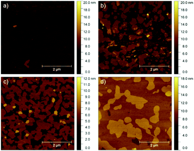 |
| | Fig. 1 AFM height images of evaporated NDI-C9 ultrathin films of different nominal thicknesses of (a) 2.0 nm, (b) 4.0 nm, (c) 7.0 nm, and (d) 10.0 nm (the z-scale is adjusted to indicate each specific layer by the same color in all images). | |
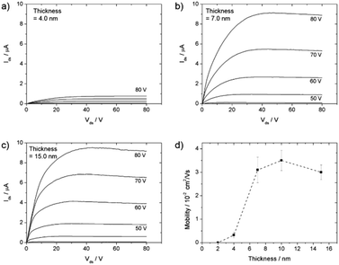 |
| | Fig. 2 Output characteristics of transistors with plain evaporated NDI-C9, recorded at different gate voltages for film thicknesses of (a) 4.0 nm, (b) 7.0 nm, and (c) 15.0 nm, and (d) electron mobility/thickness dependence. | |
Table 1 Average working parameters of OFETs with evaporated NDI-C9 ultrathin films
| NDI-C9 thickness |
μ
e/cm2 V−1 s−1 |
V
th,e/V |
| 2.0 |
— |
— |
| 4.0 |
0.3 × 10⁻² |
36 |
| 7.0 |
3.1 × 10⁻² |
35 |
| 10.0 |
3.6 × 10⁻² |
30 |
| 15.0 |
3.0 × 10⁻² |
25 |
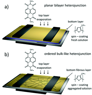 |
| | Fig. 3 Illustration of transistors with (a) bilayer and (b) ordered bulk-like heterojunction structures. Both morphologies are based on bottom spin-coated P3HT and evaporated NDI-C9 top layers. | |
 |
| | Fig. 4 Output characteristics at different gate voltages of bilayer OFETs consisting of spin-coated P3HT bottom layers of thicknesses of (a) 14.0 nm and (b) 6.0 nm spin-coated from pristine solution and 15.0 nm evaporated NDI-C9 top layers. | |
 |
| | Fig. 5 (a) Output characteristics at different gate voltages of a transistor with an ordered bulk-like heterojunction structure consisting of a bottom spin-coated 6.0 nm P3HT fiber network and an evaporated 15.0 nm NDI-C9 top layer, and (b) the square root of the transfer characteristics of the corresponding OFETs. Given mobilities correspond to these specific output plots. | |
Table 2 Average working parameters of OFETs with NDI-C9 top layers of different thicknesses evaporated on 6.0 nm thin P3HT fibrous networks spin-coated from aggregated solution
| P3HT thickness |
μ
h/cm2 V−1 s−1 |
μ
e/cm2 V−1 s−1 |
V
th,h/V |
V
th,e/V |
| 6.0 |
1.7 × 10⁻² |
3.0 × 10⁻² |
−10 |
37 |
| 8.0 |
1.2 × 10⁻² |
2.0 × 10⁻² |
−13 |
25 |
| 10.0 |
7.2 × 10⁻³ |
1.6 × 10⁻² |
−7 |
28 |
| 14.0 |
1.0 × 10⁻² |
1.0 × 10⁻² |
−7 |
14 |
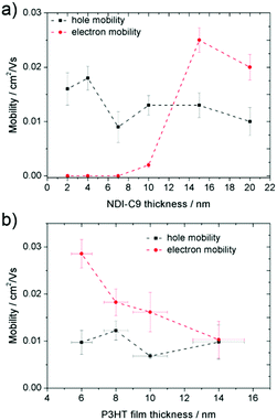
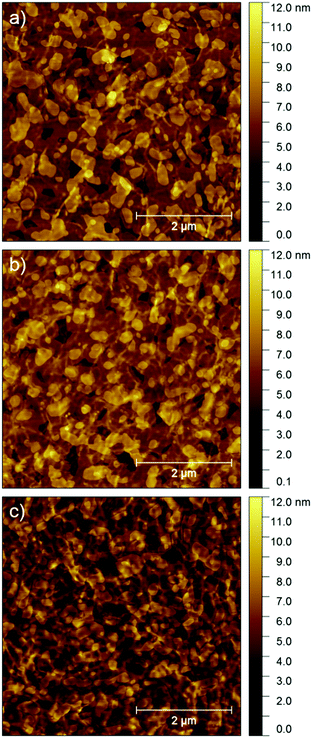
TOF SIMS of the P3HT/NDI-C9 surface was performed to confirm if naphthalene molecules penetrated the fibrous network and planar layer of P3HT (Fig. 6). The surface of a 10 nm thick P3HT layer, either uniform or fibrous depending on the type of solution, covered with thermally evaporated 15 nm thick NDI-C9 film was inspected with respect to the reference sample of pure P3HT cast from the pristine solution, for which a vivid peak from C3H3S+ ions was clearly visible. The signal from these cations was used as an indicator for the P3HT presence on the film top surface. In the case of NDI-C9 evaporated on the pristine, non-aggregated P3HT layer, the signal from C3H3S+ ions was absent indicating that the small molecules fully cover the P3HT layer. When NDI-C9 was evaporated on the P3HT fibrillar layer, a clear C3H3S+ signal was detected proving that that NDI-C9 does not form a uniform film at the P3HT layer due to penetration of NDI-C9 molecules into hollow spaces between the P3HT fibers. For further confirmation, a series of samples with an approx. 6 nm thick aggregated P3HT layer and NDI-C9 evaporated films of thicknesses varying from 2 to 20 nm was investigated in terms of microstructure and electrical properties. Fig. 7 shows the AFM height images of the thin P3HT fibrous network gradually filled by NDI-C9 molecules. The OFET characteristics of these structures (Table 2 and Fig. 8a) revealed that the hole mobility is independent of the thickness of the NDI-C9 layer. Samples with nominal NDI-C9 layer thicknesses of 2, 4, and 7 nm showed no electron transport, despite the fact that the transistors based on pure 4 nm thin evaporated NDI-C9 exhibited an n-type mobility of 3.3 × 10⁻³ cm2 V−1 s−1 (Fig. 2). It was found that deposition of the NDI-C9 layer with a nominal thickness of 10 nm was required in the case of the P3HT fibrous network to ensure similar electron transport. This observation can be explained by the larger amount of NDI-C9 necessary to form a continuous layer due to the presence of the P3HT fibers separating the NDI-C9 domains. It is worth mentioning also, that the smooth HMDS treated SiO2 dielectric surface led to a lower density of electron trapping sites in comparison to the rough P3HT fiber interface. AFM images presented in Fig. 9 with marked NDI-C9 regions (orange color) and spaces between these islands (blue color) showed that evaporation of a 4.0 nm thin NDI-C9 layer on the HDMS modified SiO2 dielectric was sufficient for completion of, at least, the first monolayer (Fig. 9b). The same amount of NDI-C9 molecules evaporated on a 6 nm thin P3HT fiber network resulted in evident discontinuities between the NDI-C9 islands (Fig. 9a).
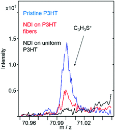 |
| | Fig. 6 TOF SIMS surface spectra of spin-coated pristine uniform (non aggregated) P3HT film with and without evaporated NDI-C9 (15 nm thick) as well as NDI-C9 evaporated on the P3HT fiber network (15 nm thick). | |
 |
| | Fig. 7 AFM height images of ultrathin films based on 6.0 nm aggregated P3HT fiber networks with evaporated NDI-C9 layers of different nominal thicknesses of (a) 2.0 nm, (b) 4.0 nm, (c) 7.0 nm, and (d) 15.0 nm. | |
 |
| | Fig. 8 Mobility as a function of thickness for OFETs with (a) constant 6.0 nm P3HT fiber networks and different thicknesses of NDI-C9 top layers, and (b) different thicknesses of P3HT fiber networks and constant 15.0 nm NDI-C9 top layers. | |
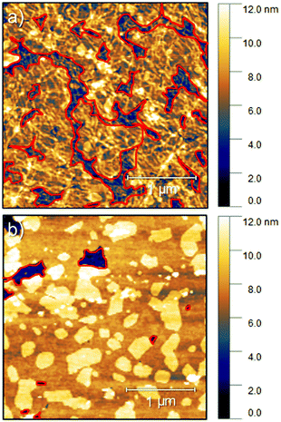 |
| | Fig. 9 AFM height images of a 4.0 nm thick NDI-C9 layer evaporated on (a) a P3HT fiber network (6.0 nm), and (b) a HMDS modified SiO2 dielectric. Blue areas enveloped by red lines indicate the discontinuities in the NDI-C9 layers. | |
To investigate the influence of the thickness of the P3HT fibrous network on the microstructure and charge transport of the ambipolar transistors, the P3HT thickness was varied from 6 to 14 nm keeping the nominal thickness of the evaporated NDI-C9 layer unchanged at 15 nm (Fig. 10). Fig. 10b and Table 3 present the charge carrier mobility as a function of P3HT film thickness. The hole mobility remained almost constant within the investigated thickness range. At the same time, a gradual decrease of the electron mobility was noticed. These observations support the previous claim that NDI-C9 molecules penetrate the thicker fiber network less effectively, so that a lower amount of the n-type material can be deposited directly at the dielectric interface.
 |
| | Fig. 10 AFM images of 15.0 nm thick NDI-C9 layers evaporated on the P3HT fiber networks obtained from aggregated solution of thicknesses of (a) 6.0 nm, (b) 8.0 nm, and (c) 14.0 nm. | |
Table 3 Average working parameters of OFETs with 15.0 nm thick evaporated NDI-C9 top layers and bottom P3HT fibrous networks of different thicknesses obtained from aggregated solution
| NDI-C9 thickness |
μ
h/cm2 V−1 s−1 |
μ
e/cm2 V−1 s−1 |
V
th,h/V |
V
th,e/V |
| 2.0 |
1.6 × 10⁻² |
— |
−29 |
— |
| 4.0 |
1.8 × 10⁻² |
— |
−21 |
— |
| 7.0 |
1.0 × 10⁻² |
— |
35 |
— |
| 10.0 |
1.3 × 10⁻² |
0.2 × 10⁻² |
10 |
40 |
| 15.0 |
1.7 × 10⁻² |
2.2 × 10⁻² |
−5 |
35 |
| 20.0 |
0.9 × 10⁻² |
1.9 × 10⁻² |
−20 |
20 |
To gain more information about the molecular order, grazing incidence wide-angle X-ray scattering (GIWAXS) was performed. However, due to the very low film thickness, only weak X-ray scattering was observed making these data inconclusive. In order to achieve stronger X-ray scattering signals from the GIWAXS measurements, thicker samples were prepared. P3HT films of 80 nm thickness were spin-cast onto HMDS treated substrates from aged and pristine solutions. The GIWAXS patterns indicted a significantly higher crystallinity for the aged P3HT, which confirmed an increased molecular order in the fibrils (Fig. S6 and S7, ESI†). Subsequently, 60 nm of NDI-C9 was evaporated on these aged and fresh P3HT films. Interestingly, NDI-C9 showed also a higher crystallinity when evaporated on the fibrillar morphology of aged P3HT in comparison to molecules sublimed on the continuous P3HT film obtained from fresh solution (Fig. S6 and S7, ESI†), whereby the crystal lattices for the polymer and NDI-C9 remained unchanged (Table S1, ESI†). Although these results for thicker samples might not fully reflect the molecular structure in ultrathin films, they indicated that the increased electron mobility of the bulk-like heterojunction was also related to the improved molecular order of NDI-C9.
Conclusions
Ultrathin, ambipolar films based on p-type semiconducting P3HT and n-type small molecule NDI-C9 were fabricated and investigated as active layers in OFETs. Solution processed bulk heterojunction binary blends obtained from one solution required a high excess of NDI-C9 to ensure balanced hole and electron transport. Despite the symmetric device operation, the mobilities were only on the order of 10−3 cm2 V−1 s−1 and the thicknesses of these films significantly exceeded the ultrathin range. Bilayers consisting of thermally evaporated NDI-C9 on top of the P3HT layers spin-coated from pristine solution exhibited also ambipolar behaviour, but the electron transport was strongly deteriorated by the roughness of the P3HT/NDI-C9 interface. To enhance the electron transport by a smooth interface between P3HT and NDI-C9 layers, the thickness of the P3HT layer was reduced to 6 nm; however, this resulted in deterioration of the hole transport. Therefore, to improve the performance of the ambipolar transistors, a novel approach to fabricate P3HT/NDI-C9 binary structures was applied. Thereby, the microstructure of the ultrathin P3HT film was changed from a continuous layer spin-coated from pristine solution to a highly structured fibrous network processed from an aggregated one. The n-type NDI-C9 molecules were then thermally evaporated on top of the fibrous P3HT network. The inspection of the film microstructure revealed that the NDI-C9 molecules partially penetrated the spaces between the fibers leading to a structured bulk-like heterojunction morphology with the n-type phase also located close to the dielectric interface. Transistors based on such microstructures exhibited a balanced mobility on the order of 10−2 cm2 V−1 s−1 for both types of charge carriers. A systematic variation of the thicknesses of the P3HT and NDI-C9 layers confirmed that better electron transport was achieved when the n-type layer was close to the dielectric interface, what is in agreement with recent literature on small molecular bilayer compounds.45 The combination of solution processing of a p-type polymer fiber network with the evaporation of n-type small molecules represents an alternative concept for the fabrication of ambipolar heterojunction transistors. The advantage of this approach is continuity of both phases due to the self-assembly of the molecules improving the transport of charge carriers. This type of processing might also have potential for organic photovoltaics if the molecular orientation can be controlled to favour charge transport in the direction perpendicular to the substrate.
Conflicts of interest
There are no conflicts to declare.
Acknowledgements
This work was supported by the National Science Centre, Poland, through grants DEC-2013/08/M/ST5/00914, UMO-2015/18/E/ST3/00322 and UMO-2016/22/E/ST5/00472. The authors thank Dr Krzysztof Kolman for DFT calculations of the HOMO/LUMO energy levels. Polish countrywide license for Biovia Materials Studio (ICM, University of Warsaw) provided by Wroclaw Centre for Networking and Supercomputing is acknowledged. Open Access funding provided by the Max Planck Society.
References
- J. Mei, Y. Diao, A. L. Appleton, L. Fang and Z. Bao, J. Am. Chem. Soc., 2013, 135, 6724–6746 CrossRef PubMed.
- O. Ostroverkhova, Chem. Rev., 2016, 116, 13279–13412 CrossRef PubMed.
- A. W. Hains, Z. Liang, M. A. Woodhouse and B. A. Gregg, Chem. Rev., 2010, 110, 6689–6735 CrossRef PubMed.
- M. L. Chabinyc and A. Salleo, Chem. Mater., 2004, 16, 4509–4521 CrossRef.
- L. Zhang, C.-a. Di, G. Yu and Y. Liu, J. Mater. Chem., 2010, 20, 7059–7073 RSC.
- A. C. Arias, J. D. MacKenzie, I. McCulloch, J. Rivnay and A. Salleo, Chem. Rev., 2010, 110, 3–24 CrossRef PubMed.
-
D. R. Gamota, P. Brazis, K. Kalyanasundaram and J. Zhang, Printed organic and molecular electronics, Springer Science & Business Media, 2013 Search PubMed.
- H. Xu, Q. Zhu, T. Wu, W. Chen, G. Zhou, J. Li, H. Zhang and N. Zhao, Appl. Phys. Lett., 2016, 109, 213301 CrossRef.
- Y. Xu, C. Liu, D. Khim and Y.-Y. Noh, Phys. Chem. Chem. Phys., 2015, 17, 26553–26574 RSC.
- Y. Zhao, Y. Guo and Y. Liu, Adv. Mater., 2013, 25, 5372–5391 CrossRef PubMed.
- H. T. Nicolai, M. Kuik, G. A. H. Wetzelaer, B. de Boer, C. Campbell, C. Risko, J. L. Brédas and P. W. M. Blom, Nat. Mater., 2012, 11, 882–887 CrossRef PubMed.
- K. Zhou, H. Dong, H.-L. Zhang and W. Hu, Phys. Chem. Chem. Phys., 2014, 16, 22448–22457 RSC.
- S. Cho, J. K. Lee, J. S. Moon, J. Yuen, K. Lee and A. J. Heeger, Org. Electron., 2008, 9, 1107–1111 CrossRef.
- S.-S. Cheng, P.-Y. Huang, M. Ramesh, H.-C. Chang, L.-M. Chen, C.-M. Yeh, C.-L. Fung, M.-C. Wu, C.-C. Liu, C. Kim, H.-C. Lin, M.-C. Chen and C.-W. Chu, Adv. Funct. Mater., 2014, 24, 2057–2063 CrossRef.
- F. Dinelli, R. Capelli, M. A. Loi, M. Murgia, M. Muccini, A. Facchetti and T. J. Marks, Adv. Mater., 2006, 18, 1416–1420 CrossRef.
- W. Li and H. L. Kwok, Thin Solid Films, 2012, 520, 3600–3604 CrossRef.
- D. Khim, G.-S. Ryu, W.-T. Park, H. Kim, M. Lee and Y.-Y. Noh, Adv. Mater., 2016, 28, 2752–2759 CrossRef PubMed.
- S. Wang, A. Kiersnowski, W. Pisula and K. Müllen, J. Am. Chem. Soc., 2012, 134, 4015–4018 CrossRef PubMed.
- A. Dodabalapur, L. Torsi and H. E. Katz, Science, 1995, 268, 270 CrossRef PubMed.
- Y. Zhang, L. Zhang, H. Liu, D. Sun and X. Li, CrystEngComm, 2015, 17, 1453–1463 RSC.
- J. Feng, Y. Zhang, C. Zhao, R. Li, W. Xu, X. Li and J. Jiang, Chem. – Eur. J., 2008, 14, 7000–7010 CrossRef PubMed.
- S. Fomine, L. Fomina, V. Garcia and R. Gaviño, Polymer, 1998, 39, 6415–6421 CrossRef.
- H. Sirringhaus, Adv. Mater., 2005, 17, 2411–2425 CrossRef.
- X. Xu, T. Xiao, X. Gu, X. Yang, S.-V. Kershaw, N. Zhao, J. Xu and Q. Miao, ACS Appl. Mater. Interfaces, 2015, 7, 28019–28026 CrossRef PubMed.
- I. Frac, M. Kucinska, P. Gawrys, M. Zagorska, W. Maniukiewicz, A. Nosal, J. Ulanski and M. Gazicki-Lipman, Synth. Met., 2016, 220, 194–201 CrossRef.
- C. Liu, L. Yun, M.-V. Lee, A. Kumatani and K. Tsukagoshi, Phys. Chem. Chem. Phys., 2013, 15, 7917–7933 RSC.
- M. Wiatrowski, E. Dobruchowska, W. Maniukiewicz, U. Pietsch, J. Kowalski, Z. Szamel and J. Ulanski, Thin Solid Films, 2010, 518, 2266–2270 CrossRef.
- S. R. Puniredd, A. Kiersnowski, G. Battagliarin, W. Zajaczkowski, W. W. H. Wong, N. Kirby, K. Mullen and W. Pisula, J. Mater. Chem. C, 2013, 1, 2433–2440 RSC.
- Q. Wei, K. Tajima and K. Hashimoto, ACS Appl. Mater. Interfaces, 2009, 1, 1865–1868 CrossRef PubMed.
- S. Cho, J. Yuen, J. Y. Kim, K. Lee, A. J. Heeger and S. Lee, Appl. Phys. Lett., 2008, 92, 063505 CrossRef.
- H.-S. Seo, M.-J. An, Y. Zhang and J.-H. Choi, J. Phys. Chem. C, 2010, 114, 6141–6147 CrossRef.
- T. Jung, B. Yoo, L. Wang, A. Dodabalapur, B. A. Jones, A. Facchetti, M. R. Wasielewski and T. J. Marks, Appl. Phys. Lett., 2006, 88, 183102 CrossRef.
- A. Baskaran and P. Smereka, J. Appl. Phys., 2012, 111, 044321 CrossRef.
- S.-W. Liu, C.-C. Lee, H.-L. Tai, J.-M. Wen, J.-H. Lee and C.-T. Chen, ACS Appl. Mater. Interfaces, 2010, 2, 2282–2288 CrossRef.
- Y.-Y. Liu, C.-L. Song, W.-J. Zeng, K.-G. Zhou, Z.-F. Shi, C.-B. Ma, F. Yang, H.-L. Zhang and X. Gong, J. Am. Chem. Soc., 2010, 132, 16349–16351 CrossRef PubMed.
- J. W. Shi, H. B. Wang, D. Song, H. K. Tian, Y. H. Geng and D. H. Yan, Adv. Funct. Mater., 2007, 17, 397–400 CrossRef.
- L. Janasz, M. Gradzka, D. Chlebosz, W. Zajaczkowski, T. Marszalek, A. Kiersnowski, J. Ulanski and W. Pisula, Langmuir, 2017, 33, 4189–4197 CrossRef PubMed.
- U. Bielecka, P. Lutsyk, K. Janus, J. Sworakowski and W. Bartkowiak, Org. Electron., 2011, 12, 1768–1776 CrossRef.
- M. Chang, J. Lee, N. Kleinhenz, B. Fu and E. Reichmanis, Adv. Funct. Mater., 2014, 24, 4457–4465 CrossRef.
- A. R. Aiyar, J.-I. Hong, J. Izumi, D. Choi, N. Kleinhenz and E. Reichmanis, ACS Appl. Mater. Interfaces, 2013, 5, 2368–2377 CrossRef PubMed.
- L. Janasz, D. Chlebosz, M. Gradzka, W. Zajaczkowski, T. Marszalek, K. Mullen, J. Ulanski, A. Kiersnowski and W. Pisula, J. Mater. Chem. C, 2016, 4, 11488–11498 RSC.
- P. Kohn, Z. Rong, K. H. Scherer, A. Sepe, M. Sommer, P. Müller-Buschbaum, R. H. Friend, U. Steiner and S. Hüttner, Macromolecules, 2013, 46, 4002–4013 CrossRef.
- M. Hufnagel and M. Thelakkat, J. Polym. Sci., Part B: Polym. Phys., 2016, 54, 1125–1136 CrossRef.
- L. Janasz, A. Luczak, T. Marszalek, B. G. R. Dupont, J. Jung, J. Ulanski and W. Pisula, ACS Appl. Mater. Interfaces, 2017, 9, 20696–20703 CrossRef PubMed.
- S. Hunag, B. Peng and P. K. L. Chan, Adv. Electron. Mater., 2017, 3, 1700268 CrossRef.
Footnote |
| † Electronic supplementary information (ESI) available: AFM images and profiles, hysteresis of electric measurements, GIWAXS patterns, integrations and structural parameters. See DOI: 10.1039/c8tc01502c |
|
| This journal is © The Royal Society of Chemistry 2018 |
Click here to see how this site uses Cookies. View our privacy policy here. 
 Open Access Article
 This Open Access Article is licensed under a
  c,
Dorota
Chlebosz
c,
Dorota
Chlebosz