
 Open Access Article
 This Open Access Article is licensed under a
 Creative Commons Attribution 3.0 Unported Licence
Compositionally tunable ternary Bi2(Se1−xTex)3 and (Bi1−ySby)2Te3 thin films via low pressure chemical vapour deposition†
Sophie L.
Benjamin
ab,
C. H. (Kees)
de Groot
c,
Chitra
Gurnani
ad,
Samantha L.
Hawken
a,
Andrew L.
Hector
 a,
Ruomeng
Huang
*c,
Marek
Jura
e,
William
Levason
a,
Eleanor
Reid
a,
Gillian
Reid
*a,
Stephen P.
Richards
a and
Gavin B. G.
Stenning
e
a,
Ruomeng
Huang
*c,
Marek
Jura
e,
William
Levason
a,
Eleanor
Reid
a,
Gillian
Reid
*a,
Stephen P.
Richards
a and
Gavin B. G.
Stenning
e
aChemistry, University of Southampton, Southampton SO17 1BJ, UK. E-mail: G.Reid@soton.ac.uk
bSchool of Science and Technology, Nottingham Trent University, Nottingham NG11 8NS, UK
cElectronics and Computer Science, University of Southampton, Southampton SO17 1BJ, UK. E-mail: R.Huang@soton.ac.uk
dSchool of Natural Sciences, Mahindra Ecole Centrale, Hyderabad, India
eISIS Neutron and Muon Source, Rutherford Appleton Laboratory, Harwell Science and Innovation Campus, Didcot, OX11 0QX, UK
First published on 12th July 2018
Abstract
The inherently rapid ligand substitution kinetics associated with the novel and chemically compatible precursors, [MCl3(EnBu2)3] (M = Sb, Bi; E = Se, Te), enable CVD growth of ternary Bi2(Se1−xTex)3 and (Bi1−ySby)2Te3 thin films with very good compositional, structural and morphological control, for the first time. X-ray diffraction data follow Vegard's law and Raman bands shift linearly with the atom substitutions, indicating very well-distributed solid solutions.
Antimony and bismuth selenide and telluride, M2E3 (M = Sb, Bi; E = Se, Te), are layered narrow bandgap semiconductors; Bi2Se3 0.24 eV, Bi2Te3 0.16 eV and Sb2Te3 0.28 eV.1,2 Their highly anisotropic hexagonal structures lead to a number of important properties. M2E3 are of particular interest as thermoelectric materials for near room temperature applications. n-Type Bi2Te3 and p-type Sb2Te3 may be used to produce thermoelectric generators if coupled electrically in series and thermally in parallel.3–6 Thermoelectric materials typically require high electrical conductivities, whilst being thermally insulating. Electrical conductivities (σ) reported for the layered hexagonal M2E3 materials produced via a range of deposition methods are ∼100–550 S cm−1 (Bi2Se3),7 ∼340–1780 S cm−1 (Bi2Te3)8–12 and 104–1695 S cm−1 (Sb2Te3).13–15 Sb2Se3, on the other hand, adopts an orthorhombic structure and with its comparatively larger band gap (1.1 eV), has intrinsically low electrical conductivity (10−6–10−7 S cm−1),16 however, its high absorption coefficient (>105 cm−1)17 and dielectric constant (29–18 within a 2 kHz to 2 MHz range)18 are attractive for photovoltaics.19,20 These materials are also important topological insulators21,22 and candidates for spintronic devices.14
As a scalable and relatively inexpensive processing method, chemical vapour deposition (CVD) is very widely used for thin film deposition.23 A number of CVD approaches have been employed for binary M2E3 film growth, most of which use multiple precursor sources, e.g. Bi2Se3: BiMe3 + SeEt2/H2;7 Bi2Te3: BiMe3 + TeiPr2;8 Sb2Te3: SbR3 (R = Me, Et) + TeR2 (R = Et, iPr).24,25 However, single source precursors (containing the metal and chalcogen within a single molecule) can offer advantages, including good control of the film stoichiometry, more efficient precursor use, and easier-to-handle precursors (less hydrolytically sensitive and less pyrophoric). A small number of single source precursors for CVD of binary M2E3 materials have been reported, including [Bi{(SePR2)2N}3] (R = Ph, iPr),26,27 whilst [Sb{(TePiPr2)2N}3]28 and [Sb{SeC5H3(Me-3)N}3]29 have been used to deposit Sb2Te3 and Sb2Se3, respectively, via aerosol assisted (AA)CVD. [MeSb(EnBu2)2] (E = Se, Te) produce Sb2Se3 and Sb2Te3 thin films via low pressure (LP)CVD.13,30 We have used molecular complexes of early transition metal and main group chlorides, bearing neutral chalcogenoether ligands for LPCVD of binary metal chalcogenide thin films.31–34 The possibility of selective deposition of oriented films onto defined regions of lithographically patterned substrates has also been realised using these types of precursors.12 This selectivity could bring significant advantages in device fabrication, since, if the chalcogenide material can be deposited only onto pre-defined regions of patterned substrates, this would reduce the number of processing steps required (e.g. removing the need for back-etching), as well as reducing the volume of the chalcogenide material required.
Whilst commercial thermoelectric devices based upon n-type Bi2Te3 and p-type Sb2Te3 are available, significantly enhanced thermoelectric properties have been reported for ternary phases and superlattices of Bi2Te3 and Sb2Te3.35,36 The ability to control the composition, morphology and crystallite sizes in thin films of the related ternary materials is therefore of considerable interest to allow optimisation of their properties for various applications, most notably thermoelectrics and topological insulators.37–41 For n-type Bi2Te3, this is best achieved by introducing Se, forming a solid solution of Bi2(Se1−xTex)3. Optimisation of p-type Sb2Te3 can be achieved by incorporation of Bi, in (Bi1−ySby)2Te3. Previous work has mainly involved solid state or solution processing methods to produce the ternary materials, and usually as bulk materials rather than thin films.35–41 CVD of thin films of these key ternary thin film materials with good compositional control, as well as structural/morphological control, would open up exciting application prospects. However, this is particularly challenging by conventional CVD methods involving multiple precursors.
We report here the new molecular precursors, [BiCl3(SenBu2)3], [SbCl3(SenBu2)3] and [SbCl3(TenBu2)3], demonstrate their utility as single source CVD precursors for binary Bi2Se3, Sb2Se3 and Sb2Te3 films, respectively, and, most significantly, we show that LPCVD using the appropriate combination of (chemically similar) precursors from this series, produces thin films of the two key ternary solid solutions, Bi2(Se1−xTex)3 and (Bi1−ySby)2Te3 with very good compositional, structural and morphological control.
Precursors
Whilst a number of CVD reagents for Bi2Se3 thin film deposition are known (vide supra), the previously unknown analogues of the precursor we used to deposit Bi2Te3, i.e. [BiCl3(TenBu2)3], were prepared with the intention of achieving chemical compatibility between the precursor types. The target compounds, [BiCl3(SenBu2)3], [SbCl3(SenBu2)3] and [SbCl3(TenBu2)3], were obtained in good yield as illustrated in Scheme 1, and have been shown to be suitable for LPCVD of the respective binary M2E3 thin films, with compositional, structural and electrical properties indicative of high quality materials (ESI†).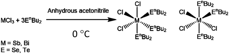 | ||
| Scheme 1 Synthesis of the precursor complexes. | ||
We have shown previously that n-type Bi2Te3 can be selectively deposited into the TiN wells of lithographically patterned TiN/SiO2 substrates using the precursor [BiCl3(TenBu2)3],12 therefore, it was important to establish whether this could also be achieved for the p-type Sb2Te3. SEM images from depositions using ∼15 mg of [SbCl3(TenBu2)3] at 723 K revealed that this is indeed the case (Fig. 1a). Quantitative EDX analysis revealed an Sb![[thin space (1/6-em)]](https://www.rsc.org/images/entities/char_2009.gif) :Te ratio of 41%:59% and grazing incidence XRD data are consistent with R-3mH Sb2Te3 (Fig. 1b).
:Te ratio of 41%:59% and grazing incidence XRD data are consistent with R-3mH Sb2Te3 (Fig. 1b).
 | ||
| Fig. 1 (a) SEM image with EDX mapping and (b) grazing incidence XRD pattern from Sb2Te3 selectively deposited from [SbCl3(TenBu2)3] into 30 μm TiN holes and an indexed bulk pattern of Sb2Te3.42 The TiN substrate peaks are marked by *. | ||
LPCVD of ternary Bi2(Se1−xTex)3 thin films
Our approach to deposit thin films of the ternary chalcogenide, Bi2(Se1−xTex)3, exploits the inherent high lability of Bi(III) complexes with neutral donor ligands in solution. We have utilised the rapid ligand substitution kinetics of [BiCl3(EnBu2)3] (E = Se, Te) to create mixed telluroether/selenoether complexes of BiCl3 by combining various ratios of the precursors in CH2Cl2 solution prior to the CVD experiments. The relatively similar temperatures required for LPCVD of each of the binary M2E3 phases from this homologous pair of precursors was also promising for the LPCVD of the required Bi2(Se1−xTex)3 ternary phase. At first sight, the need for a higher temperature for the Bi2Se3 deposition (550 °C) from [BiCl3(SenBu2)3] in comparison to that for LPCVD growth of Bi2Te3 (450 °C) was unexpected. However, this most likely reflects the presence of the weaker Te–C bonds in the latter (cf. the Se–C bonds in [BiCl3(SenBu2)3]), arising from the orbital energy mismatch of the C and Te atoms. Hence, while the volatility of the higher MWt [BiCl3(TenBu2)3] precursor is expected to be lower than for the [BiCl3(SenBu2)3] precursor, this is offset by its lower thermal stability.To test the hypothesis that these two precursors would be compatible for the optimisation of the target ternary Bi2(Se1−xTex)3 phase by LPCVD, we initially studied the solution behaviour of [BiCl3(TenBu2)3] and [BiCl3(SenBu2)3], and mixtures thereof, by 77Se{1H} and 125Te{1H} NMR spectroscopy in CH2Cl2 solution (Fig. S7, ESI†). Each of solutions (i) to (iv) gave only one singlet at room temperature, indicating a rapidly exchanging mixture in solution. Introducing increasing amounts of [BiCl3(TenBu2)3] to a solution of [BiCl3(SenBu2)3] leads to a progressive shift of δ(77Se) to lower frequency, while δ(125Te) moves to higher frequency (cf. the individual parent complexes). Lowering the temperature to −80 °C causes only slight broadening of the resonances for each of the parent complexes (i) and (iv), and this was replicated for the mixed Se/Te samples ((ii) and (iii)). This behaviour is consistent with rapid ligand exchange (scrambling) in CH2Cl2 solution and the high lability of the BiCl3 acceptor fragment, suggesting that the species present in solution are of the form [BiCl3{(SenBu2)1−m(TenBu2)m}3] (m = 0 to 1) and hence this may be a possible reagent for LPCVD of the target ternary Bi2(Se1−xTex)3 phase.
To test this hypothesis, a series of LPCVD experiments were undertaken by mixing different ratios of the two precursors to produce [BiCl3{(SenBu2)1−a(TenBu2)a}3] with different values of a (from 0 to 3). Depositions were performed at 550 °C/0.05 mmHg onto SiO2-coated silicon substrates. In each case, reflective silvery films were obtained. EDX analyses (Fig. 2) revealed that the %Te content increases with increasing Te precursor amount, with a concomitant decrease in the %Se present. These data indicate very good control of the composition of the Bi2(TexSe1−x)3 ternary material using the [BiCl3(TenBu2)3]/[BiCl3(SenBu2)3] precursor system. The %Te does not increase linearly with the fraction of the Te precursor used. Instead, it shows an enhancement in Te deposition. The enhancement factor can be calculated by the Te precursor fraction using eqn (1),
 | (1) |
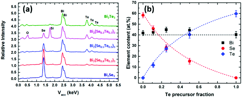 | ||
| Fig. 2 (a) EDX spectra and (b) relationship between film composition and fraction of [BiCl3(TenBu2)3] used in the deposition of ternary Bi2(Se1−xTex)3 films. | ||
SEM (Fig. 3) analysis shows that the ternary films, like the binary parent materials, are polycrystalline, with good coverage across the substrate. In each case, film thicknesses of ca. 1 μm were obtained. The hexagonal crystallites are clearly visible, although their orientation varies; for the Bi2Se3 films, the crystallites appear to be aligned perpendicular to the substrate, whereas in the ternary and Bi2Te3 films most of the crystallites tend to lie parallel to the surface.
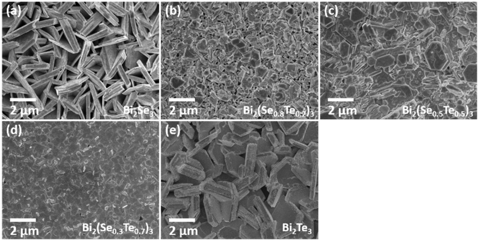 | ||
| Fig. 3 SEM images showing the morphologies of the Bi2Se3 (a), Bi2Te3 (e) and ternary Bi2(Se1−xTex)3 (b–d) films deposited by LPCVD under similar conditions (550 °C/0.05 mmHg) onto SiO2-coated silicon substrates. | ||
The phase purity and crystallinity of the as-deposited films were examined by grazing incidence XRD analysis (Fig. 4a). All five films are isostructural, with no other phases detectable. A systematic shift of all the characteristic diffraction peaks with increasing Te composition is evident. Broadening of the 015 peak (Fig. 4b) for the Bi2(Se0.8Te0.2)3, Bi2(Se0.5Te0.5)3, Bi2(Se0.3Te0.7)3 films can be observed, consistent with increased disorder in the structures due to Te doping. This disorder is also consistent with the decrease of the crystallite sizes for these three ternary compositions seen in Fig. 3. The lattice parameters (a, c) of all five compositions were refined against the Bi2Se3 phase from the ICSD.43 Linear increases of both a and c with increasing Te content are observed (Fig. 4c), consistent with Vegard's law, i.e. well distributed solid solutions of the ternary Bi2(Se1−xTex)3.
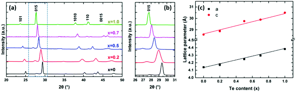 | ||
| Fig. 4 (a) XRD patterns of as-deposited Bi2(Se1−xTex)3 films with x ranging from 0 to 1; (b) expanded XRD patterns showing the systematic shift of the 015 peak; (c) refined lattice parameters (see Table S1, ESI†) as a function of the Te content for different as-deposited Bi2(Se1−xTex)3 films. | ||
The vibrational properties of the as-deposited Bi2(Se1−xTex)3 films were also studied by Raman spectroscopy. The spectra are shown in Fig. 5, where peaks are fitted using the Gaussian equation. For Bi2Se3 (Fig. 5a), two peaks positioned at 129 and 171 cm−1 can be assigned as E2g (in-plane) and A21g (out-of-plane) modes, respectively, similar to previous reports.44 These two vibrational modes are also present in the other four films, although they shift progressively to lower wavenumbers with increasing Te content (Fig. 5f). These results provide strong evidence for a very well-distributed solid solution.38,39 An additional peak at ca. 120 cm−1 is detected for Bi2(Se0.3Te0.7)3 and Bi2Te3 (Fig. 5d and e), ascribed to the A1u mode, which is IR-active. The appearance of this peak implies the breaking of the crystal symmetry in the third dimension due to the limited thickness and the presence of the interfaces.45,46
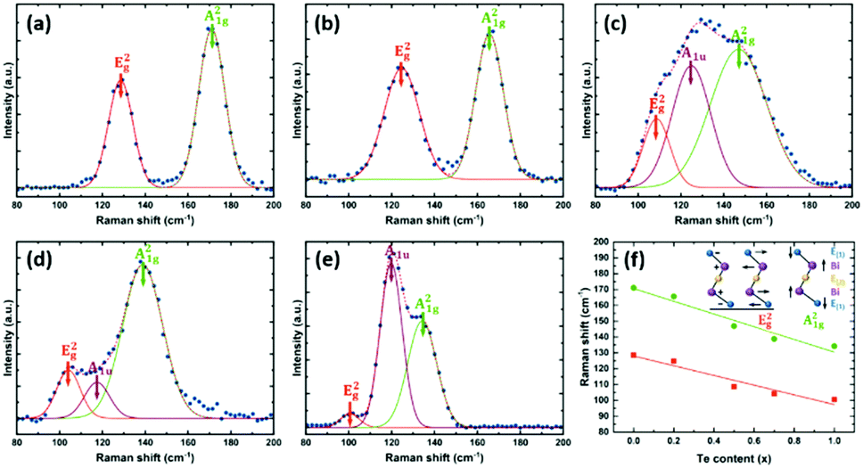 | ||
| Fig. 5 (a–e) Raman spectra of as-deposited Bi2(Se1−xTex)3 films with x ranging from 0 to 1. (f) Phonon frequencies (orange: E2g mode; green: A21g mode) as a function of Te composition. The inset provides the schematic diagrams for the two Raman-active modes. | ||
LPCVD of (Bi1−ySby)2Te3 thin films
To ascertain the compatibility of the precursors required for the target ternary (Bi1−ySby)2Te3 thin films, various ratios of [MCl3(TenBu2)3] (M = Bi and Sb) were analysed by 125Te{1H} NMR spectroscopy in CH2Cl2. In all cases, just one Te resonance was observed, consistent with the TenBu2 ligands being labile and freely exchanging between the two weakly Lewis acidic MCl3 units. A gradual change in chemical shift is observed with increasing Bi content, from 237 ppm for pure [SbCl3(TenBu2)3], to 262 ppm for pure [BiCl3(TenBu2)3].In order to deposit the target ternary (Bi1−ySby)2Te3 films, different ratios of the [BiCl3(TenBu2)3] and [SbCl3(TenBu2)3] precursors were combined. In a typical LPCVD experiment, ca. 60 mg total mass of the reagents were combined in the chosen ratio, and the deposition was performed at 500 °C onto SiO2 substrates, leading to silver-grey films across several substrates. Temperature profiling of the furnace revealed that when set to 500 °C, there was a temperature gradient from 270 °C at the edge of the furnace to 496 °C in the centre. Analysis of the films by XRD, EDX, SEM and Raman spectroscopy revealed that there was a variation in composition across the substrates, with increasing Sb content at higher deposition temperatures. The following analysis focuses on the films with the best coverage and showing a clear compositional variation with deposition temperature (across an 8 °C range from 474–482 °C), with the composition changing from Bi-rich at the cooler end, to Sb rich at the hotter end.
EDX analysis (Fig. 6a) was used to map the composition along the length of the sample (as a function of deposition temperature). Fig. 6b shows the change in %Sb content with temperature across the substrate; moving from lower to higher temperature the Bi content decreases. It also shows that the Sb-rich phases deposit within a very narrow temperature range. It is clear that Bi2Te3 deposits more easily at lower temperatures than Sb2Te3 and consequently, the Bi content in the vapour phase of the precursor is depleted in the early stages of the hot zone, which means it does not reach the substrates at higher temperatures.
 | ||
| Fig. 6 (a) EDX spectra and (b) relationship between (Bi1−ySby)2Te3 film composition and the increasing temperature of deposition (indicating the temperatures at positions A, B and C). | ||
SEM images (Fig. 7) taken at three positions (A–C) across the substrate show that the morphology is rather different from the regular hexagonal morphology observed for either Bi2Te3 or Sb2Te3. Moving along the substrate to the more Sb-rich phase, individual irregular-shaped plate-like crystallites are observed, rather than regular hexagons.
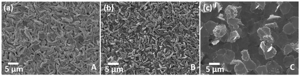 | ||
| Fig. 7 SEM images of three regions (A–C) of the film deposited from a 1:1 ratio of [SbCl3(TenBu2)3] and [BiCl3(TenBu2)3] from Sb poor (a) to Sb rich (c). | ||
Grazing incidence XRD data (Fig. 8) are consistent with a single phase (with no elemental Te) and show the reflections gradually shift from a lower 2θ value for Bi2Te3 to a higher 2θ value with increasing Sb content, as expected. The variation in the lattice parameters with Sb content is shown in Fig. 8c. Whilst the lattice parameter change is smaller in this system, there is an approximately linear trend, consistent with Vegard behaviour.
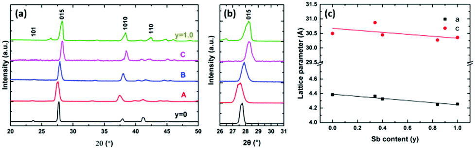 | ||
| Fig. 8 (a) Grazing incidence XRD patterns from 3 positions (A–C; Sb poor to Sb rich) of a ternary sample deposited from a 1:1 ratio of [SbCl3(TenBu2)3] and [BiCl3(TenBu2)3], together with the binary phases (Sb2Te3 and Bi2Te3). Position A: a = 4.370(11) and c = 30.80(8) Å, position B: a = 4.327(8) and c = 30.54(8) Å, position C: a = 4.249(9) and c = 30.29(8) Å. (b) Expanded XRD patterns showing the systematic shift of the 015 peak; (c) refined lattice parameters as a function of the Sb content for different as-deposited (Bi1−ySby)2Te3 films. | ||
The composition of the film was also mapped with Raman spectroscopy (Fig. 9). This shows the shift in peaks from Bi2Te3 to Sb2Te3. The E2g vibrational mode shifts from 100 to 120 cm−1 and the E21g mode shifts from 134 to 167 cm−1 showing the change in composition of the solid solution of the ternary phase. This is consistent with Raman spectra of (Bi1−ySby)2Te3 deposited by solvothermal synthesis47 and MBE.37
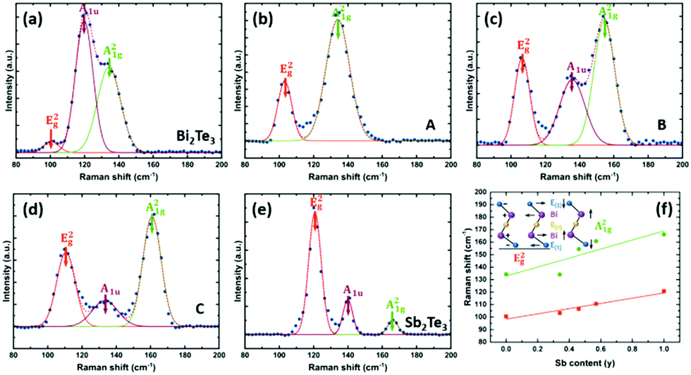 | ||
| Fig. 9 (a–e) Raman spectra from 3 positions (Sb poor to Sb rich) of a ternary (Bi1−ySby)2Te3 sample deposited from a 1:1 ratio of [SbCl3(TenBu2)3] and [BiCl3(TenBu2)3], together with the binary phases (Sb2Te3 and Bi2Te3); (f) phonon frequencies (orange: E2g mode; green: A21g mode) as a function of Sb composition. The inset provides the schematic diagrams for the two Raman-active modes. | ||
Conclusions
This work presents a chemically compatible library of molecular precursors suitable for the LPCVD growth of high quality binary M2E3 (M = Sb, Bi; E = Se, Te) thin films on silica. Moreover, their suitability to be combined in different ratios, producing rapidly scrambling precursor systems, allows a highly innovative route for the LPCVD of the key ternary Bi2(Se1−xTex)3 and (Bi1−ySby)2Te3 films with very good compositional, structural and morphological control, as well-distributed solid solutions (following Vegard behaviour). In the case of Bi2(Se1−xTex)3, the ternary composition is mainly governed by the relative ratios of the precursors used, whilst for (Bi1−ySby)2Te3, the deposition temperature has a greater influence on the film composition.Good compositional, structural and morphological control across the ternary phase is very important for tuning the functional properties of the V–VI materials for applications in thermoelectric devices or topological insulators. This, coupled with the demonstration that our precursor system allows selective film growth onto defined regions of lithographically patterned substrates, suggests that using these new precursors in a CVD based approach offers exciting prospects for the fabrication of thin film micro-thermoelectric generators. This will form the basis of our future work.
Conflicts of interest
There are no conflicts to declare.Acknowledgements
We thank the STFC for funding (ST/L003376/1 and ST/P00007X/1) and the EPSRC for a Case Award to S. L. H. (EP/M50662X/1). We also gratefully acknowledge funding for thin film diffraction and NMR instrumentation from the EPSRC through EP/K00509X, EP/K009877/1 and EP/K039466/1. C. G. thanks the Royal Society (London) for a Newton International Alumnus Award.Notes and references
- O. Madelung, Semiconductors: Data Handbook, Springer Berlin Heidelberg, Berlin Heidelberg, 2004, vol. 14 Search PubMed.
- T. C. Harman, B. Paris, S. E. Miller and H. L. Goering, J. Phys. Chem. Solids, 1957, 2, 181–190 CrossRef.
- G. J. Snyder and E. S. Toberer, Nat. Mater., 2008, 7, 105–114 CrossRef PubMed.
- L. E. Bell, Science, 2008, 321, 1457–1461 CrossRef PubMed.
- V. A. Kutasov, L. N. Lukyanova and M. V. Vedernikov, in Thermoelectrics Handbook: Macro to Nano, ed. R. D. Michael, CRC Press, 2006, ch. 37 Search PubMed.
- C. J. Vineis, A. Shakouri, A. Majumdar and M. G. Kanatzidis, Adv. Mater., 2010, 22, 3970–3980 CrossRef PubMed.
- A. Al Bayaz, A. Giani, A. Foucaran, F. Pascal-Delannoy and A. Boyer, Thin Solid Films, 2003, 441, 1–5 CrossRef.
- H. You, S. H. Baek, K.-C. Kim, O.-J. Kwon, J.-S. Kim and C. Park, J. Cryst. Growth, 2012, 346, 17–21 CrossRef.
- A. Akrap, A. Ubaldini, E. Giannini and L. Forro, EPL, 2014, 107, 57008 CrossRef.
- M. M. Rashid, K. H. Cho and G.-S. Chung, Appl. Surf. Sci., 2013, 279, 23–30 CrossRef.
- N. Peranio, M. Winkler, Z. Aabdin, J. König, H. Böttner and O. Eibl, Phys. Status Solidi A, 2012, 209, 289–293 CrossRef.
- S. L. Benjamin, C. H. de Groot, C. Gurnani, A. L. Hector, R. Huang, E. Koukharenko, W. Levason and G. Reid, J. Mater. Chem. A, 2014, 2, 4865–4869 RSC.
- S. L. Benjamin, C. H. de Groot, A. L. Hector, R. Huang, E. Koukharenko, W. Levason and G. Reid, J. Mater. Chem. C, 2015, 3, 423–430 RSC.
- S. Zastrow, J. Gooth, T. Boehnert, S. Heiderich, W. Toellner, S. Heimann, S. Schulz and K. Nielsch, Semicond. Sci. Technol., 2013, 28, 035010 CrossRef (6 pages).
- P. Fan, Z. H. Zheng, G. X. Liang, D. P. Zhang and X. M. Cai, J. Alloys Compd., 2010, 505, 278–280 CrossRef.
- L. R. Gilbert, B. Van Pelt and C. Wood, J. Phys. Chem. Solids, 1974, 35, 1629–1632 CrossRef.
- Y. Zhou, M. Leng, Z. Xia, J. Zhong, H. Song, X. Liu, B. Yang, J. Zhang, J. Chen, K. Zhou, J. Han, Y. Cheng and J. Tang, Adv. Energy Mater., 2014, 4, 1301846 CrossRef.
- C. Chen, D. C. Bobela, Y. Yang, S. Lu, K. Zeng, C. Ge, B. Yang, L. Gao, Y. Zhao, M. C. Beard and J. Tang, Front. Optoelectron., 2017, 10, 18–30 CrossRef.
- Y. C. Choi, T. N. Mandal, W. S. Yang, Y. H. Lee, S. H. Im, J. H. Noh and S. Il Seok, Angew. Chem., Int. Ed., 2014, 53, 1329–1333 CrossRef PubMed.
- X. Liu, J. Chen, M. Luo, M. Leng, Z. Xia, Y. Zhou, S. Qin, D. J. Xue, L. Lv, H. Huang, D. Niu and J. Tang, ACS Appl. Mater. Interfaces, 2014, 6, 10687–10695 CrossRef PubMed.
- H. Zhang, C.-X. Liu, X.-L. Qi, X. Dai, Z. Fang and S. C. Zhang, Nat. Phys., 2009, 5, 438–442 Search PubMed.
- Y. Guo, Z. Liu and H. Peng, Small, 2015, 11, 3290–3305 CrossRef PubMed.
- A. C. Jones and M. L. Hitchman, in Chemical Vapour Deposition: Precursors, ed. A. C. Jones and M. L. Hitchman, The Royal Society of Chemistry, 2009, pp. 1–36 Search PubMed.
- A. Giani, A. Boulouz, F. P. Delannoy, A. Foucaran, A. Boyer, B. Aboulfarah and A. Mzerd, J. Mater. Sci. Lett., 1999, 18, 541–543 CrossRef.
- J. H. Kim, Y. C. Jung, S. H. Suh and J. S. Kim, J. Nanosci. Nanotechnol., 2006, 6, 3325–3328 CrossRef PubMed.
- J. Waters, D. Crouch, J. Raftery and P. O’Brien, Chem. Mater., 2004, 16, 3289–3298 CrossRef.
- J. Waters, D. Crouch, P. O’Brien and J. H. Park, J. Mater. Sci.: Mater., 2003, 4, 599–602 Search PubMed.
- S. S. Garje, D. J. Eisler, J. S. Ritch, M. Afzaal, P. O’Brien and T. Chivers, J. Am. Chem. Soc., 2006, 128, 3120–3121 CrossRef PubMed.
- R. K. Sharma, G. Kedarnath, V. K. Jain, A. Wadawale, M. Nalliath, C. G. S. Pillai and B. Vishwanadh, Dalton Trans., 2010, 39, 8779–8787 RSC.
- R. Huang, S. L. Benjamin, C. Gurnani, Y. Wang, A. L. Hector, W. Levason, G. Reid and C. H. de Groot, Sci. Rep., 2016, 6, 27593 CrossRef PubMed (10 pages).
- S. D. Reid, A. L. Hector, W. Levason, G. Reid, B. J. Waller and M. Webster, Dalton Trans., 2007, 4769–4777 RSC.
- C. H. de Groot, C. Gurnani, A. L. Hector, R. Huang, M. Jura, W. Levason and G. Reid, Chem. Mater., 2012, 24, 4442–4449 CrossRef.
- K. George, C. H. de Groot, C. Gurnani, A. L. Hector, R. Huang, M. Jura, W. Levason and G. Reid, Chem. Mater., 2013, 25, 1829–1836 CrossRef.
- S. L. Benjamin, C. H. de Groot, C. Gurnani, A. L. Hector, R. Huang, K. Ignatyev, W. Levason, S. J. Pearce, F. Thomas and G. Reid, Chem. Mater., 2013, 25, 4719–4724 CrossRef PubMed.
- R. Venkatasubramanian, E. Siivola, T. Colpitts and B. O’Quinn, Nature, 2001, 413, 597–602 CrossRef PubMed.
- X. Guo, X. Jia, K. Jie, H. Sun, Y. Zhang, B. Sun and H. Ma, CrystEngComm, 2013, 15, 7236–7242 RSC.
- C. Weyrich, M. Drögeler, J. Kampmeier, M. Eschbach, G. Mussler, T. Merzenich, T. Stoica, I. E. Batov, J. Schubert, L. Plucinski, B. Beschoton, C. M. Schneider, C. Stampfer, D. Grüzmacher and T. Tchäpers, J. Phys.: Condens. Matter, 2016, 28, 495501 CrossRef PubMed.
- M. Hong, T. C. Chasapis, Z.-G. Chen, L. Yang, M. G. Kanatzidis, J. Snyder and J. Zou, ACS Nano, 2016, 10, 4719–4727 CrossRef PubMed.
- A. Soni, Z. Yanyuan, Y. Ligen, M. K. K. Aik, M. S. Dresselhaus and Q. Ziong, Nano Lett., 2012, 12, 1203–1209 CrossRef PubMed.
- J.-L. Mi, P. Norby, M. Bremholm and B. B. Iversen, Chem. Mater., 2017, 29, 5070–5079 CrossRef.
- B. Xu, T. Feng, M.-T. Agne, L. Zhou, X. Ruan, G. J. Snyder and Y. Wu, Angew. Chem., Int. Ed., 2017, 56, 3546–3551 CrossRef PubMed.
- T. L. Anderson and H. B. Krause, Acta Crystallogr., 1974, B30, 1307–1310 CrossRef.
- ICSD: Inorganic Crystal Structure Database (ICSD), Fachinformationszentrum Karlsruhe (FIZ), accessed via the EPSRC National Chemical Database Service hosted by the Royal Society of Chemistry.
- (a) A. J. Barton, N. J. Hill, W. Levason, B. Patel and G. Reid, Chem. Commun., 2001, 95–96 RSC; (b) A. J. Barton, N. J. Hill, W. Levason and G. Reid, J. Chem. Soc., Dalton Trans., 2001, 1621–1627 RSC.
- D. Teweldebrhan, V. Goyal and A. A. Balandin, Nano Lett., 2010, 10, 1209–1218 CrossRef PubMed.
- K. M. F. Shahil, M. Z. Hossain, D. Teweldebrhan and A. A. Balandin, Appl. Phys. Lett., 2010, 96, 153103 CrossRef.
- C. Zhang, Z. Peng, Z. Li, L. Yu, K. A. Khor and Q. Xiong, Nano Energy, 2015, 15, 688–696 CrossRef.
Footnote |
| † Electronic supplementary information (ESI) available: Methods for the precursor syntheses and characterisation, LPCVD experiments and film characterisation, together with discussion of the binary M2E3 film characterisation and electrical properties. See DOI: 10.1039/c8tc01285g |
| This journal is © The Royal Society of Chemistry 2018 |