
 Open Access Article
 This Open Access Article is licensed under a Creative Commons Attribution-Non Commercial 3.0 Unported Licence
Roll to roll atmospheric pressure plasma enhanced CVD of titania as a step towards the realisation of large area perovskite solar cell technology
J. L.
Hodgkinson
 *a,
H. M.
Yates
a,
A.
Walter
b,
D.
Sacchetto
b,
S.-J.
Moon
b and
S.
Nicolay
b
*a,
H. M.
Yates
a,
A.
Walter
b,
D.
Sacchetto
b,
S.-J.
Moon
b and
S.
Nicolay
b
aMaterials and Physics Research Centre, University of Salford, Cockcroft Building, Manchester, M5 4WT, UK. E-mail: j.l.hodgkinson@salford.ac.uk
bCentre Suisse d’Electronique et de Microtechnique (CSEM), PV-Center, Jaquet-Droz 1, 2002 Neuchâtel, Switzerland
First published on 1st February 2018
Abstract
Atmospheric pressure plasma enhanced CVD (AP PECVD) systems have attracted considerable interest in recent years due to the significant benefits for large area, low cost substrates and low temperature operation. In this work we describe the use of a bespoke roll to roll AP PECVD process to produce large area, functional TiO2−x films for use as hole blocking electron transport layers in perovskite solar cell architectures, a critical component typically produced by spin coating or vacuum based technologies. The AP PECVD produced films can be used to construct cells with overall efficiencies greater than from the sputtered reference material (13.57 vs. 13.15% maximum power point for 1 cm2 cells). Discussion of the cell properties suggests scope for further optimisation, maximising the potential of this approach.
Introduction
The application of low temperature, non-equilibrium ‘technological’ plasmas has attracted much interest in recent years due to their widespread potential.1 Core applications include surface modification1,2 and deposition processes,3,4 alongside catalysis5,6 and growing areas such as plasma medicine.7,8 The common need to produce plasmas over large areas at atmospheric pressure is most readily achieved by the use of a dielectric barrier system9–11 and such an approach has previously been applied for surface modification and the activation of deposition processes such as CVD.However the application to functional inorganic materials has been limited due to compromised film properties compared to established technologies. A significant factor is that dielectric barrier systems operating at atmospheric pressure typically result in a filamentary discharge which impacts on film uniformity,12,13 and may cause substrate damage14 or pinholes in the film. A more suitable diffuse discharge is observed in helium attributed to the relatively long lifetime of its metastable states15,16 and small radius,9 but the cost limits large scale application. It has been shown that a visually diffuse discharge may be achieved in commodity gases such as argon and nitrogen via the optimisation of reactor geometry and the development of audio17,18 and more recently, pulsed DC19 and modulated RF power supplies.20 The choice of power supply, the resultant discharge mode and the impact on film properties remain the subject of intensive research.9,21 A second, highly topical, area of research is the optimisation of solid state organic–inorganic hybrid perovskite solar cells.22 These structures utilise relatively abundant materials to achieve high efficiencies with typical values of 20% reported for optimised, sub 1 cm2, examples.23 A critical component of most reported architectures is the electron transport layer (ETL) which extracts photogenerated electrons from the perovskite and transports these charges to electrodes.24 The ETL also serves as a hole blocking layer, preventing re-combination of holes generated in the perovskite with electrons in the transparent conducting oxide (TCO) electrode. The ETL layer, typically TiO2, needs to be compact, defect free and conformal to avoid poor performance.
This layer is usually produced by spin coating25 or vacuum processes such as conventional ALD26 or magnetron sputtering. These have the disadvantages of either only being suited to small area or having high start-up and running costs, with additional issues associated with batch processing. By use of an atmospheric pressure, low temperature, in-line process wide area uniform coatings are potentially possible at reduced costs and increased simplicity of engineering. CVD is well known for its capabilities to produce such coatings and the ease of integration within industry.27,28
In previous work the authors have studied the deposition of TiO2 at low temperatures via atmospheric pressure PECVD, driven by both sinusoidal29 and sub microsecond pulsed DC30 power supplies. Whilst it was found that a range of film properties could be achieved, these studies were conducted using static (batch) reactor systems, which could not provide the level of uniformity or size required for this application. In this work, we describe the use of our bespoke roll to roll atmospheric pressure PECVD system to produce TiO2−x films over large areas (10 cm × 10 cm), highlighting the scalability of this approach and potential for in-line processing. The films are characterised, applied to a commercial TCO and used to construct mesoscopic perovskite solar cells. The viability of the AP PECVD process is shown by comparison with a sputtered TiO2−x ETL over a full evaluation of cell properties.
Experimental
Film growth
The TiO2−x films were deposited at ambient temperature using the laboratory scale roll to roll system depicted schematically in Fig. 1. This unit features a dual laminar flow design to minimise the entrainment of surrounding air and provide two reaction zones to improve net growth rate and uniformity over a line width of 22 cm. Each reaction zone incorporates a dielectric barrier system to provide plasma activation and extraction of waste products to avoid contamination. The film thickness was controlled by the number of passes under the coating head. The roll to roll system may be used to convey solid substrates up to 20 × 20 cm to provide dynamic coating and simulate a continuous production process. In this work, 10 cm × 10 cm substrates were used to suit the cell fabrication process. TiO2−x films were deposited on 3 mm float glass and a commercial F:SnO2 (FTO), TCO22-15 supplied by Solaronix. Titanium(IV) isopropoxide (TTIP) (≥97% Aldrich) was delivered via a conventional bubbler at a rate of 5 × 10⁻⁵ mol min−1 with a total process gas flow of 14.6 L min−1. Argon (99.998% BOC) was used throughout with plasma activation being provided by an in house developed audio frequency power supply. This unit operates at a resonant frequency in the order of 3.2 kHz and features high frequency suppression to attenuate the current spikes associated with a filamentary discharge,15 helping to maintain a diffuse discharge. Films were deposited at a line speed of 10.69 m h−1 with applied voltages of 4, 8 and 10 kV. Film thickness was determined by the number of passes under the coating head.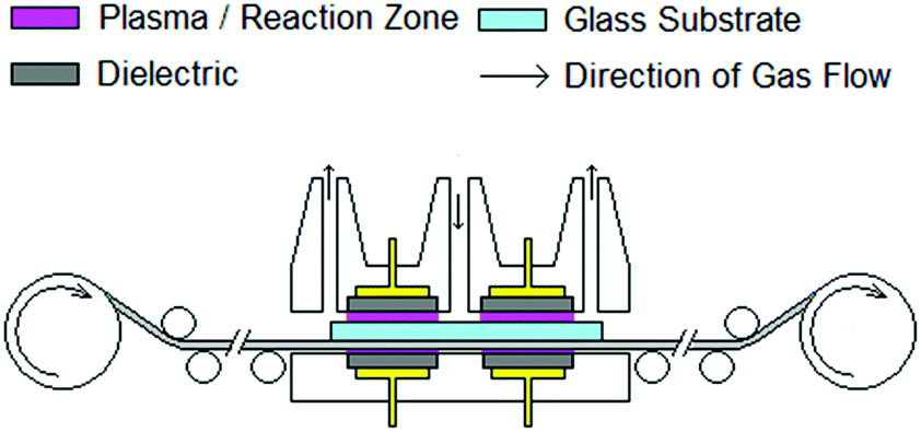 | ||
| Fig. 1 Schematic showing the roll to roll AP PECVD unit. | ||
The AP PECVD TiO2−x films were compared to reference TiO2−x films with 23 nm thickness deposited by RF sputtering at 60 °C in argon with oxygen added at a partial pressure of 7.5 × 10⁻⁶ mbar.
Cell fabrication
The mesoporous TiO2 (m-TiO2) layer was deposited on the TiO2−x blocking layers/FTO coated substrates by spin coating TiO2 paste (Sharechem SC-HT040) diluted in isopropanol (TiO2 paste![[thin space (1/6-em)]](https://www.rsc.org/images/entities/char_2009.gif) :isopropanol = 1:5 weight ratio) at 4500 rpm for 30 s annealed at 500 °C for 30 minutes. 461 mg of PbI2, 159 mg of CH3NH3I, and 78 mg of DMSO (molar ratio 1:1:1) were mixed in 600 mg of dimethylformamide (DMF) solution at room temperature with stirring for 1 h in order to prepare the CH3NH3PbI3 precursor solution. The precursor solution was spin coated on m-TiOx substrate in a two-stage sequence (1000 rpm for 10 s followed by 5000 rpm for 45 s) and 0.75 ml of diethyl ether were dripped on the substrate 12 s before the end of the procedure. The substrate was then heated at 50 °C for 2 min and 100 °C for 10 min,31 spiro-MeOTAD solution was prepared by dissolving 72.3 mg spiro-MeOTAD (Merck), 28.8 μl 4-tert-butylpyridine (TCI), 17.5 μl of a stock lithium bis(trifluoromethylsulfonyl)imide (LiTFSI, Sigma-Aldrich) solution (520 mg LiTFSI in 1 ml acetonitrile) in 1 ml chlorobenzene and spin coated on top of perovskite layer at 4000 rpm for 30 s. The cells were then finished with the evaporation of a 100 nm thick gold electrode.
:isopropanol = 1:5 weight ratio) at 4500 rpm for 30 s annealed at 500 °C for 30 minutes. 461 mg of PbI2, 159 mg of CH3NH3I, and 78 mg of DMSO (molar ratio 1:1:1) were mixed in 600 mg of dimethylformamide (DMF) solution at room temperature with stirring for 1 h in order to prepare the CH3NH3PbI3 precursor solution. The precursor solution was spin coated on m-TiOx substrate in a two-stage sequence (1000 rpm for 10 s followed by 5000 rpm for 45 s) and 0.75 ml of diethyl ether were dripped on the substrate 12 s before the end of the procedure. The substrate was then heated at 50 °C for 2 min and 100 °C for 10 min,31 spiro-MeOTAD solution was prepared by dissolving 72.3 mg spiro-MeOTAD (Merck), 28.8 μl 4-tert-butylpyridine (TCI), 17.5 μl of a stock lithium bis(trifluoromethylsulfonyl)imide (LiTFSI, Sigma-Aldrich) solution (520 mg LiTFSI in 1 ml acetonitrile) in 1 ml chlorobenzene and spin coated on top of perovskite layer at 4000 rpm for 30 s. The cells were then finished with the evaporation of a 100 nm thick gold electrode.
Characterisation
The AP PECVD TiO2−x films were characterised via X-ray photoelectron spectroscopy (Kratos Axis Nova), with experimental data processed using the ‘Casa XPS’ software package. The scans were calibrated using the C 1s binding energy of 285 eV. The crystallographic structure was assessed by both X-ray diffraction (Siemens D5000) and Raman spectroscopy using a 532 nm laser as described previously,32 Film thicknesses were measured by masking the substrate with ‘Kapton’ polyimide tape and measuring the resultant step using a ‘Dektak 3ST’ surface profiler. Coverage of the substrate was assessed via SEM imaging (Philips ESEM FEG XL30). Surface roughness RMS values were obtained by atomic force microscopy (NanoScope IIIa, Digital Inst. Ltd). The sheet resistance of the films was measured using a Jandel Universal four point probe. Reflection and transmission values were measured simultaneously between 400 and 800 nm using a visible/near IR fiber optic spectrophotometer (Ocean Optics, USB 2000+) and the associate ‘SpectraSuite’ software. Haze measurements were taken using a lab built spectrometer consisting of a 75 W xenon lamp, integrating sphere and four broadband filters centring on four wavelengths (800, 650, 531, and 450 nm). The dark conductivity of the TiO2−x layer on glass was assessed after evaporating two metallic contacts on the surface. The measurements were performed under 1 mbar N2 atmosphere and in the dark. During the measurement, the temperature was ramped up from room temperature to 180 °C with a rate of 10 °C min−1 then the sample is slowly cooled down at a rate of 1 °C min−1. The conductivity was taken during the cool down phase for a more precise temperature measurement.Cell evaluation
All cells were characterized under a two-lamp class AAA WACOM sun simulator with an AM 1.5G irradiance spectrum at 1000 W m−2. The cell area was defined using a metal mask. The I–V characteristics of the cells were obtained under both reverse (from VOC to JSC) and forward (from JSC to VOC) bias. A Maximum Power Point (MPP) tracking was usually performed to extract the stabilized power output. External Quantum Efficiency (EQE) spectra were acquired on a custom-made spectral response setup equipped with a xenon lamp, a grating monochromator and lock-in amplifiers.Results and discussion,
The TiO2−x films deposited by AP PECVD were adherent under rubbing or vigorous washing. A simple scratch test using a weighted stylus gave a scratch width in the order of 30 μm for the plasma deposited film compared to 65 μm for a control film deposited without plasma activation, suggesting a significant difference in hardness. The uniformity over the 10 cm × 10 cm float glass substrate under the correct deposition conditions was similar to a comparable thermal CVD system, indicated by the presence of a single interference colour when produced on the FTO substrate. Films deposited directly on glass were relatively colourless due to the contribution of film thickness and refractive index contrast between glass and TiO2−x and hence more difficult to see by eye.SEM imaging of the surface indicated that a continuous film had been produced providing complete coverage of the surface. Fig. 2 shows the surface of a TCO22-15 sample where the left side was masked prior to coating with TiO2−x to allow the surface coverage to be more clearly seen.
 | ||
| Fig. 2 SEM image showing the TiO2−x layer on the TCO22-15 substrate. The left hand side was masked to show contrast. | ||
XPS was used to characterise the TiO2−x films deposited using applied voltages of 4, 8 and 10 kV. A soft, greasy sample deposited with zero applied voltage, and hence no plasma was included as a control. In each case, the wide scan showed clear signals attributed to carbon, titanium and oxygen species. The high resolution C 1s signal could be fitted to 3 separate curves. The most intense for adventitious elemental carbon, was used to calibrate the measurement to 285 eV in each case. The other, much smaller, signals at 286.6 eV and 289.1 eV were attributed to surface adsorbed C–OH and C![[double bond, length as m-dash]](https://www.rsc.org/images/entities/char_e001.gif) O species respectively.33 The high resolution Ti 2p spectra (Fig. 3a) could be de-convoluted into four component peaks, with 2p3/2 at 458.8 eV and 2p1/2 464.5 eV showing spin orbital splitting in the order of 5.7 eV, indicative of Ti4+ attached to O2−.34 The minor components at 462.8 eV and 457.4 eV were assigned to the presence of Ti3+,35 establishing the sub-stoichiometry of the films. The O 1s spectra (Fig. 3b) showed a major peak at 530.3 eV corresponding to O2− for an oxide,35,36 with a second resolved peak centred at 531.67 eV which has previously been assigned to surface adsorbed water, hydroxyls or C–O bonded species.36 The high resolution Ti 2p data was fitted for each sample to determine quantitatively the level of stoichiometry in the films. A significant trend between the applied voltage and the change in stoichiometry (Fig. 4) showed that an increasing voltage resulted in a more stoichiometric film. The increased stoichiometry with increased applied voltage is almost certainly due to the increased plasma energy allowing a higher degree of chemical reaction for a given substrate temperature, possibly via alternative pathways afforded by the formation of excited species.37
O species respectively.33 The high resolution Ti 2p spectra (Fig. 3a) could be de-convoluted into four component peaks, with 2p3/2 at 458.8 eV and 2p1/2 464.5 eV showing spin orbital splitting in the order of 5.7 eV, indicative of Ti4+ attached to O2−.34 The minor components at 462.8 eV and 457.4 eV were assigned to the presence of Ti3+,35 establishing the sub-stoichiometry of the films. The O 1s spectra (Fig. 3b) showed a major peak at 530.3 eV corresponding to O2− for an oxide,35,36 with a second resolved peak centred at 531.67 eV which has previously been assigned to surface adsorbed water, hydroxyls or C–O bonded species.36 The high resolution Ti 2p data was fitted for each sample to determine quantitatively the level of stoichiometry in the films. A significant trend between the applied voltage and the change in stoichiometry (Fig. 4) showed that an increasing voltage resulted in a more stoichiometric film. The increased stoichiometry with increased applied voltage is almost certainly due to the increased plasma energy allowing a higher degree of chemical reaction for a given substrate temperature, possibly via alternative pathways afforded by the formation of excited species.37
 | ||
| Fig. 3 (a) Typical high resolution Ti 2p spectrum, (b) typical high resolution O 1s spectrum. | ||
 | ||
| Fig. 4 Plot showing the increase in stoichiometry with applied voltage. | ||
The sub-stoichiometry was not perceived as a disadvantage for use as a hole blocking layer within a perovskite cell, given that in separate work38 sub-stoichiometric sputtered titania had performed well in the intended cell constructions. It is suggested that the mobility of the oxygen vacancies and titanium interstitials may contribute to a reduction in series resistance regardless of the TiO2−x film being amorphous, polycrystalline or single crystal.39
On this basis, films were deposited on the TCO22-15 FTO to be evaluated in perovskite cell structures and allow comparison with use of sputtered TiO2−x. In this case an applied voltage of 4 kV was chosen as a low level of activation may be expected to minimise the risk of powder formation and particle inclusion within the hole blocking layer. Films were deposited at a line speed of 10.69 m h−1 for 4, 6 and 10 passes under the AP PECVD head, which resulted in film thicknesses of 40, 55 and 85 nm respectively.
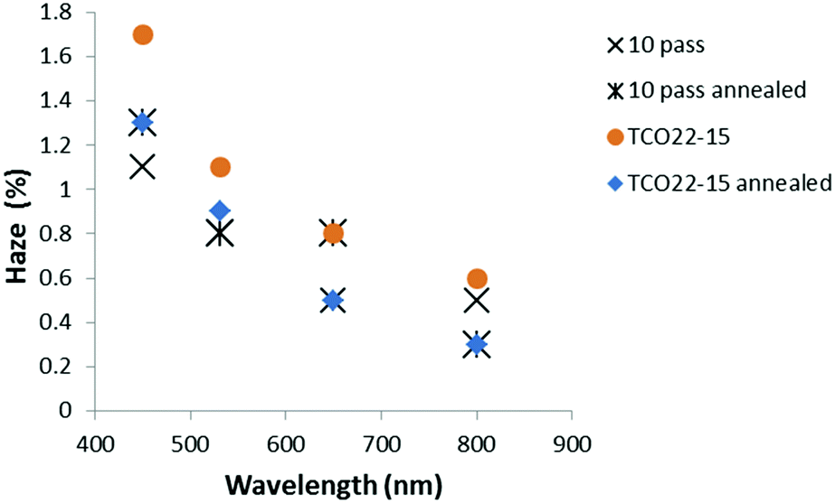
Clearly any additional transmission loss imparted by the TiO2−x layer could have an adverse effect on cell performance, hence visible region reflection and transmission measurements were taken for each film. In practice the films will form part of a multilayer cell stack, so it was considered adequate at this stage to use mean values as a comparative measure. The addition of the TiO2−x layer increased the mean reflection measured between 400 and 800 nm from 10.4% for the reference FTO to 11.3, 11.3 and 14.0% for the 4, 6 & 10 pass samples respectively. The corresponding transmission measurements also showed an increase from 80.0% for the TCO22-15, to 82 ± 1% for the TiO2−x coated samples, with a slight drop for the thickest sample as would be expected with its increased absorbance. Fig. 5 shows the collected data. Usually it would be expected that addition of extra layers would lead to a decrease in the transmission (due to increased absorbance) and a corresponding increase in reflection. While the reflection apparently follows this trend the transmission does not. It is suggested that this observation could be explained by the reduction in optical haze (Fig. 6), and the fact that the spectrometer used to simultaneously collect reflection and transmission data can only detect specular reflection, when in fact a significant proportion of the light may be scattered by the relatively rough surface of the TCO22-15. Hence whilst the measured specular reflection was increased, due to a smoother surface presented by the TiO2−x (supported by rms measurements), the total reflected light was actually reduced, enhancing transmission. The reflection data especially shows the interference fringes, with the 10 pass sample exhibiting a shorter period, confirming that it is substantially thicker than the other films and hence the over-ridding factor in the transmission is the film absorbance.
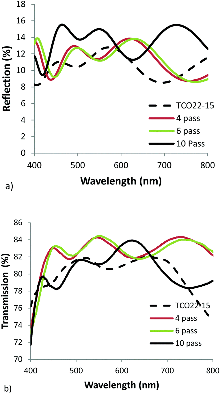 | ||
| Fig. 5 Visible region (a) reflection, and (b) transmission spectra for AP PECVD TiO2−x layers on the TCO22-15 substrate. | ||
 | ||
| Fig. 6 Measured haze values for the AP PECVD TiO2−x layers on the TCO22-15 substrate. | ||
One of the stages during cell construction involves heating the film stack to 500 °C over the course of 80 minutes. To check whether this would affect the deposited TiO2−x, an 85 nm thick TiO2−x film on FTO was annealed in a simulation of the thermal cycling experienced during cell construction.
The annealing treatment did not show any clear changes on the XRD with both the non-annealed and annealed samples only showing a single peak at 26.4° within the measured range assigned to the (110) plane of the underlying F:SnO2.40 The Raman spectra both before and after annealing, only gave broad background peaks attributed to the glass substrate. Hence for the plasma deposited samples it was considered that the annealing process was not causing a detectable modification to the originally amorphous films. However, XPS data for these samples showed a decrease in FWHM in the Ti 2p signal on annealing for both PECVD and sputtered films. Annealing of these samples reduced the 2p3/2 peak widths from 1.32 eV to 1.16 eV and 1.12 eV to 1.03 eV respectively. The reduction in FWHM has previously been related to a reduction in structural defects.41
Optical measurements suggested that the annealing process resulted in a general reduction in haze for the TCO22-15 substrate, with no change (within experimental error, SD ≤ 0.3% absolute) for the TiO2−x coated FTO samples (Fig. 7). The lesser effect for the coated samples could be accounted for by a smoother surface presented by the TiO2−x, with 4 nm rms (SD 0.3 nm) presented by the 4 pass sample (40 nm) and 6 nm rms (SD 0.4 nm) for the 10 pass sample (85 nm) compared to a roughness of 14 nm rms (SD 0.4 nm) for the TCO22-15. It was considered that this smoother surface may negate the influence of the changing TCO22-15 texture beneath. In order to determine if the change in haze was mainly due to the FTO, a TiO2−x sample (10 passes, 85 nm) on glass was annealed. In parity with the film deposited on TCO22-15, this showed limited change below 0.5% after annealing. This could be expected due to the lack of a third interface from the FTO and the fact that this film was very smooth (ca. 3 nm rms). The transmission measurements for the TiO2−x on TCO22-15 (Fig. 8) showed a significant reduction of up to 7.4% for the ten pass 85 nm film, as did the four pass 40 nm film (in the order of 2%) while the, 23 nm reference film showed negligible transmission change in agreement with its reduced thickness. However, there was minimal change on annealing for TCO22-15 suggesting that the transmission loss seen for the TiO2−x on TCO22-15 samples was due to changes within the TiO2−x film, rather than changes within the FTO. This is supported by the annealing results observed for TiO2−x deposited on float glass, with 85 nm and 40 nm thick films showing a transmission loss of 5.1 and 1.2% respectively. Such losses on annealing have been previously reported42 and attributed to light diffusion with increasing crystallite size and particle aggregation. It is suggested that the transmission loss on annealing is the result of the onset of crystal formation and associated grain boundaries within the TiO2−x layer below the detection limit of the XRD and Raman due to the relatively low thickness compared to the FTO substrate (400 nm). Such structural changes on annealing would be in agreement with the XPS observed reduction in Ti 2p3/2 peak width, which relates to a reduction in defects.
 | ||
| Fig. 7 Plot showing typical change in optical haze for TiO2−x layers on the FTO substrate with annealing. | ||
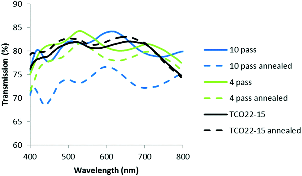 | ||
| Fig. 8 Plot showing the change in transmission with annealing. | ||
Electrical resistance presented by the TiO2−x may add undesirable series resistance to the cell. As a first indication, four point probe measurements were taken at ten points across the surface of each sample to provide an indication of the conductivity uniformity. All samples gave a relatively small variation in sheet resistance values with an average of 12.50 Ω □−1 (SD 0.16), similar to the 12.59 Ω □−1 (SD 0.11) observed for the TCO22-15 substrate, suggesting good uniform low resistivity across the film. The annealing cycle only marginally increased the measured sheet resistance to 12.85 Ω □−1 (SD 0.28) with the range of measured values overlapping that of the un-annealed sample. These values are all relatively similar, with the conductivity largely stemming from the FTO layer and hence only fractionally effected by the additional TiO2−x.
As a more accurate measure of electrical behaviour dark conductivity measurements were performed. In this case equivalent films were deposited on glass to allow the bulk property of the TiO2−x to be measured devoid of any interference form the FTO, as well as the use of evaporated electrodes avoiding penetration of the thin films. A relatively high conductivity value could be expected to more readily support charge separation and minimise the contribution to series resistance, bolstering cell performance. The dark conductivity (σ dark) results for a range of film thickness (Fig. 9) showed the AP PECVD films to have lower conductivity than the sputtered films. This is consistent also with the higher activation energy, which may indicate that these films have less oxygen deficiencies than the sputtered films.38 This is consistent with the stoichiometric ratios determined by XPS, which showed TiO1.82 for the four pass (40 nm) AP PECVD film compared to TiO1.76 for the sputtered sample. However, deconvolution of the high resolution Ti 2p spectra showed a similar proportion of Ti3+ at 3.21% and 3.37% for the AP PECVD and sputtered films respectively. It could also be envisaged that the AP PECVD films may contain a greater amount of impurities as a result of the low substrate temperature and open air processing. As shown earlier the level of disorder within the TiO2−x can be related to the broadening of the Ti 2p peak observed in the XPS spectra. In this case, comparison of the Ti 2p3/2 FWHM gave 1.32 eV for a four pass AP PECVD film and 1.12 eV for the sputtered reference, again supporting the correlation with low temperature disorder and showing advantage for the sputtered films. The σ dark measurements also showed a strong correlation with thickness suggesting a reducing conductivity for the thicker films. Changes in film structure and defect incorporation over the first few tens of nanometers have been previously reported for a CVD process43 and could apply to the described films. Given the thickness range described, such effects may be critical and further advantage could be gained by reducing the AP PECVD film thickness to match the ∼23 nm of the sputtered reference.
 | ||
| Fig. 9 (a) Dark conductivity at room temperature, (b) activation energy for a range of AP PECVD titania and the sputtered reference film on glass substrates. | ||
The AP PECVD TiOx layers on the TCO22-15 substrates were used to fabricate perovskite PV cells via the addition of a mesoporous TiO2 scaffold, perovskite, spiro-MeOTAD and Au contact as described in the Experimental section. Reference cells using TCO22-15 substrates coated with a 23 nm sputtered TiOx were constructed in parallel, this process having been previously optimised and known to give competitive cell performance. The results were highly encouraging, showing mean efficiency exceeding that of the cell constructed from the reference sputtered titania, with a comparable distribution of values.
As can been seen in Fig. 10, there is an increase in VOC, FF, JSC and hence efficiency as the thickness of the TiO2−x layer is decreased. This relates to the increased smoothness giving a better foundation for perovskite deposition and hence better electronic contact between perovskite and TiO2−x. In addition, a thicker TiO2−x film increased the series resistance, as indicated by the σ dark measurements, which reduces the ETL efficiency (although increasing its ability to act as a BL). This suggests that a thinner TiO2−x layer would improve the efficiency yet further. It should be pointed out that the reference sample has a TiO2−x thickness of only 23 nm, about half that of the AP PECVD film, so accentuates the ability of the non-optimised AP PECVD TiO2−x to produce cells of higher efficiency. The current density curves presented in Fig. 11 are consistent with an increased fill factor and reduced series resistance for the 40 nm AP PECVD and 23 nm sputtered film. The hysteresis between the forward and reverse plots is also improved in the case of the thinner films perhaps due to improved shunt resistance in the forward direction. MPP tracking confirmed that all cells were stable over 5 minutes with efficiencies around 13% for all cells with the highest value of 13.57% recorded for the 40 nm AP PECVD film followed by 13.15% for the reference.
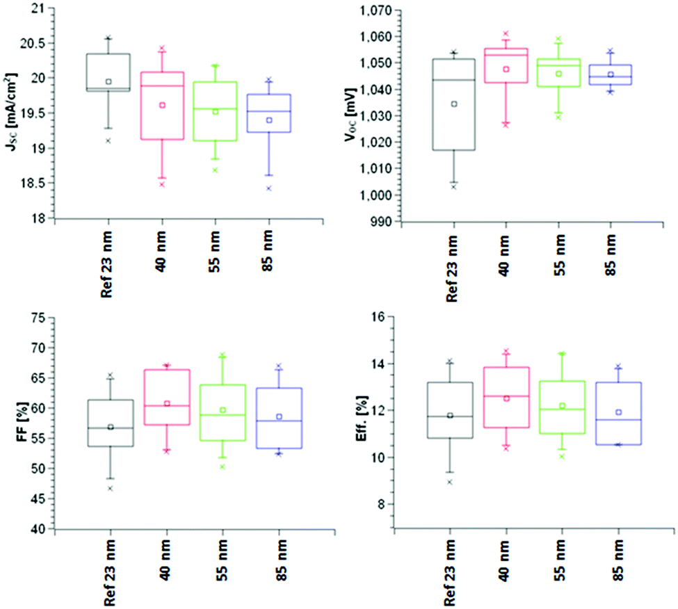 | ||
| Fig. 10 Measured cell characteristics achieved using the AP PECVD TiO2−x ETL compared to the sputtered reference. | ||
 | ||
| Fig. 11 Current density plots for the forward (red) and reverse (black) direction. | ||
There was a surprising result with the EQE measurements (Fig. 12) which showed a reduced efficiency compared to the sputtered (PVD) TiO2−x. This deficiency could be completely offset by applying a 0.5 V negative bias, suggesting that it was attributed to a collection issue related to an extraction barrier at the interface. This issue in the context of the impressive overall efficiency reinforces the scope for further optimisation of film properties.
 | ||
| Fig. 12 EQE measurements for cells fabricated using the 40 nm PE APCVD and 23 nm sputtered films. | ||
Conclusions
We have shown that atmospheric pressure plasma enhanced CVD is capable of producing sub 50 nm TiO2−x layers of sufficient quality and uniformity for use in perovskite based photovoltaic devices, with performance matching or exceeding the reference sputtered reference TiO2−x. These films were non-optimised and it was shown that a thinner film has the potential to increase cell efficiency further. Furthermore, the advantages of atmospheric pressure processing for scale-up are highlighted by the use of a continuous inline system.Conflicts of interest
There are no conflicts of interest to declare.Acknowledgements
This work was financed by Framework 7 grant FP7 NMP.2012.1.4-1 309530 PLIANT “Process line implementation for applied surface nanotechnologies” and received funding from the European Union's Horizon 2020 research and innovation programme under grant agreement No. 653296 (CHEOPS). XPS data was provided by the NEXUS national facility, with Raman kindly provided by Dr J. E. Proctor and M. Hakeen at the University of Salford.Notes and references
- C. Tendero, C. Tixier, P. Tristant, J. Desmaison and P. Leprince, Spectrochim. Acta, Part B, 2006, 61, 2 CrossRef.
- K.-Y. Cheng, C.-H. Chang, Y.-W. Yang, G.-C. Liao, C.-T. Liu and J.-S. Wu, Appl. Surf. Sci., 2017, 394, 534 CrossRef CAS.
- O. Goossens, E. Dekempeneer, D. Vangeneugden, R. Van de Leest and C. Leys, Surf. Coat. Technol., 2001, 142–144, 474 CrossRef CAS.
- R. Múgica-Vidal, F. Alba-Elías, E. Sainz-García and M. Pantoja-Ruiz, Appl. Surf. Sci., 2015, 347, 325 CrossRef.
- D. Mei, X. Zhu, C. Wu, B. Ashford, P. T. Williams and X. Tu, Appl. Catal., B, 2016, 182, 525 CrossRef CAS.
- J. C. Whitehead, The Chemistry of Cold Plasma, in Cold Plasma in Food and Agriculture, ed. N. N. Misra, O. Schlüter and P. J. Cullen, Academic Press, San Diego, 2016, ch. 3, p. 53–81 Search PubMed.
- F. Iza, G. J. Kim, S. M. Lee, J. K. Lee, J. L. Walsh, Y. T. Zhang and M. G. Kong, Plasma Processes Polym., 2008, 5, 322 CrossRef CAS.
- H. Takeshi, F. Masakazu and T. Yuichiro, Jpn. J. Appl. Phys., 2013, 52, 036201 CrossRef.
- L. Bárdos and H. Baránková, Thin Solid Films, 2010, 518, 6705 CrossRef.
- Y. Setsuhara, Arch. Biochem. Biophys., 2016, 605, 3 CrossRef CAS PubMed.
- K. N. Kim, S. M. Lee, A. Mishra and G. Y. Yeom, Thin Solid Films, 2016, 598, 315 CrossRef CAS.
- S. Martin, F. Massines, N. Gherardi and C. Jimenez, Surf. Coat. Technol., 2004, 177-178, 693 CrossRef CAS.
- R. Foest, F. Adler, F. Sigeneger and M. Schmidt, Surf. Coat. Technol., 2003, 163, 323 CrossRef.
- F. Fanelli, Surf. Coat. Technol., 2010, 205, 1536 CrossRef CAS.
- A. Bogaerts, E. Neyts, R. Gijbels and J. van der Mullen, Spectrochim. Acta, Part B, 2002, 57, 609 CrossRef.
- F. Massines, P. Segur, N. Gherardi, C. Khamphan and A. Ricard, Surf. Coat. Technol., 2003, 174–175, 8 CrossRef CAS.
- F. Massines, N. Gherardi, A. Fornelli and S. Martin, Surf. Coat. Technol., 2005, 200, 1855 CrossRef CAS.
- C. Sarra-Bournet, N. Gherardi, G. Laroche and F. Massines, Thin Solid Films, 2010, 518, 4828 CrossRef CAS.
- J. L. Walsh and M. G. Kong, Appl. Phys. Lett., 2007, 91, 221502 CrossRef.
- J. J. Shi, J. Zhang, G. Qiu, J. L. Walsh and M. G. Kong, Appl. Phys. Lett., 2008, 93, 041502 CrossRef.
- R. Bazinette, J.-F. Lelièvre, L. Gaudy and F. Massines, Energy Procedia, 2016, 92, 309 CrossRef CAS.
- S. T. Williams, A. Rajagopal, C.-C. Chueh and A. K. Y. Jen, J. Phys. Chem. Lett., 2016, 7, 811 CrossRef CAS PubMed.
- D. Bi, B. Xu, P. Gao, L. Sun, M. Grätzel and A. Hagfeldt, Nano Energy, 2016, 23, 138 CrossRef CAS.
- G. Yang, H. Tao, P. Qin, W. Ke and G. Fang, J. Mater. Chem. A, 2016, 4, 3970 CAS.
- C. X. Zhang, Y. D. Luo, X. H. Chen, W. Ou-Yang, Y. W. Chen, Z. Sun and S. M. Huang, Appl. Surf. Sci., 2016, 388, 82 CrossRef CAS.
- L. Chen, J. R. Wang, L. Q. Xie, C. Zhan, Z. Qiu, J. Z. Zhou, J. W. Yan, B. W. Mao and Z. Q. Tian, Electrochem. Commun., 2016, 68, 40 CrossRef CAS.
- R. J. McCurdy, Thin Solid Films, 1999, 351, 66 CrossRef CAS.
- D. M. Nelson, M. M. Radtke and S. E. Phillips, US Pat., 9404179, Chemical Vapor Deposition Process for Depositing a Silica Coating on a Glass Substrate, Pilkington Group Ltd, 2016 Search PubMed.
- J. L. Hodgkinson, H. M. Yates and D. W. Sheel, Plasma Processes Polym., 2009, 6, 575 CrossRef CAS.
- J. L. Hodgkinson and D. W. Sheel, Surf. Coat. Technol., 2013, 230, 73 CrossRef CAS.
- N. Ahn, D.-Y. Son, I.-H. Jang, S. M. Kang, M. Choi and N.-G. Park, J. Am. Chem. Soc., 2015, 137, 8696 CrossRef CAS PubMed.
- D. Smith, R. T. Howie, I. F. Crowe, C. L. Simionescu, C. Muryn, V. Vishnyakov, K. S. Novoselov, Y.-J. Kim, M. P. Halsall, E. Gregoryanz and J. E. Proctor, ACS Nano, 2015, 9, 8279 CrossRef CAS PubMed.
- Handbook of X-Ray Photoelectron Spectroscopy, ed. J. Chastain and R. C. King, Physical Electronic Inc., New York, 1995 Search PubMed.
- M. E. Simonsen, H. Jensen, Z. Li and E. G. Søgaard, J. Photochem. Photobiol., 2008, 200, 192 CrossRef CAS.
- P. M. Kumar, S. Badrinarayanan and M. Sastry, Thin Solid Films, 2000, 358, 122 CrossRef CAS.
- I. Stambolova, M. Shipochka, V. Blaskov, A. Loukanov and S. Vassilev, J. Photochem. Photobiol., B, 2012, 117, 19 CrossRef PubMed.
- S. Sivaram, Chemical Vapour Deposition Thermal and Plasma Deposition of Electronic Materials, Van Nostrand Reinhold, New York, 1995 Search PubMed.
- H. M. Yates, M. Afzaal, A. Walter, J. L. Hodgkinson, S.-J. Moon, D. Sacchetto, M. Brauninger, B. Niesen, S. Nicolay, M. McCarthy, M. E. Pemble, I. M. Povey and C. Ballif, J. Mater. Chem. C, 2016, 4, 11269 RSC.
- A. Moballegh and E. C. Dickey, Acta Mater., 2015, 86, 352 CrossRef CAS.
- S. Shanthi, C. Subramanian and P. Ramasamy, Mater. Sci. Eng., B, 1999, 57, 127 CrossRef.
- P. Prieto and R. E. Kirby, J. Vac. Sci. Technol., A, 1995, 13, 2819 CAS.
- M. B. Karoui, Z. Kaddachi and R. Gharbi, J. Phys.: Conf. Ser., 2015, 596, 012012 CrossRef.
- C. Calmes, D. Bouchiera, C. Clerc and Y. Zheng, Appl. Surf. Sci., 2004, 224, 122 CrossRef CAS.
| This journal is © The Royal Society of Chemistry 2018 |