
 Open Access Article
 This Open Access Article is licensed under a
 Creative Commons Attribution 3.0 Unported Licence
Controlling the electrochromic properties of conductive polymers using UV-light†
Robert
Brooke
a,
Jesper
Edberg
 a,
Donata
Iandolo
ab,
Magnus
Berggren
a,
Xavier
Crispin
a and
Isak
Engquist
*a
a,
Donata
Iandolo
ab,
Magnus
Berggren
a,
Xavier
Crispin
a and
Isak
Engquist
*a
aLinköping University, Department of Science and Technology, Laboratory of Organic Electronics, Norrköping SE-601 74, Sweden. E-mail: isak.engquist@liu.se
bDepartment of Bioelectronics, Centre Microelectronique de Provence, Ecole Nationale Superieure des Mines de Saint Etienne, 880, route de Mimet, Gardanne 13541, France
First published on 26th February 2018
Abstract
The phenomenon of electrochromism in conductive polymers is well known and has been exploited in many scientific reports. Using a newly developed patterning technique for conductive polymers, we manufactured high-resolution electrochromic devices from the complementary polymers PEDOT and polypyrrole. The technique, which combines UV-light exposure with vapor phase polymerization, has previously only been demonstrated with the conductive polymer PEDOT. We further demonstrated how the same technique can be used to control the optical properties and the electrochromic contrast in these polymers. Oxidant exposure to UV-light prior to vapor phase polymerization showed a reduction in polymer electrochromic contrast allowing high-resolution (100 μm) patterns to completely ‘disappear’ while applying a voltage bias due to their optical similarity in one redox state and dissimilarity in the other. This unique electrochromic property enabled us to construct devices displaying images that appear and disappear with the change in applied voltage. Finally, a modification of the electrochromic device architecture permitted a dual image electrochromic device incorporating patterned PEDOT and patterned polypyrrole on the same electrode, allowing the switching between two different images.
Introduction
Electrochromism refers to the change in a material's optical properties with the onset of a specific applied electrical stimulus. Devices exploiting this phenomenon have found applications in different fields, e.g., smart windows for building temperature regulation or glare reduction. With their potential to reduce energy costs and consumption through reduced air conditioning and heating, electrochromic materials have been extensively researched and developed.1,2 Other applications include electrochromic displays and adaptive IR camouflaging.3–5 Since the discovery of electrochromism in metal oxide films there have been many advancements in the field.6,7 From device architecture modifications such as multiple layers8 to material manipulations introducing composite substances,9 improvements to the field of electrochromics have been widespread.Conductive polymers (CPs) have been of interest to the electrochromic community10 due to their unique electrical and optical properties, compatibility with large-scale production, ability to be easily chemically modified and their potential to replace inorganic materials in certain electrochromic applications. CPs can be synthesized in a variety of ways including chemical,11,12 electrochemical13 and vapor phase polymerization (VPP).14–16 VPP involves the deposition of an oxidant solution followed by exposure to monomer vapour in a controlled environment. As such, VPP overcomes limitations of CP solubility, results in CPs in thin film form (<300 nm) and allows the possibility to coat a wide range of substrates, including non-conductive surfaces. By optimizing the VPP parameters, researchers have shown impressive improvements in electrical and optical properties of CPs films making them suitable for various opto-electronic applications.17–21 Films of poly(3,4-ethylenedioxythiophene) (PEDOT) with high conductivity (>1000 S cm−1), necessary for various organic electronic applications, have been reported using the VPP technique.22,23
Patterning of CPs allows an expansion of their potential to be exploited into flexible electronics. To date CP have been patterned using many strategies.24–26 Certain patterning techniques such as ultrasonic spray-coating27 and photolithography28,29 have been applied within the electrochromic field for patterned display applications. Other researchers have focused on the patterning of derivatives of common CPs30,31 or patterning into novel substrates.32,33 Recently, a novel patterning technique has been reported for PEDOT.34 The developed procedure involves a UV-light treatment of oxidant films prior to VPP, resulting in changes in both the electrical and optical properties of the obtained PEDOT film. UV-light treatment was shown to alter the chemical environment of the oxidant and therefore modify the polymerization kinetics during VPP. By employing a photomask during the exposure step, it was possible to produce patterns with features down to a resolution of 10 μm. A short summary of the previous report is supplied in the ESI.†![[thin space (1/6-em)]](https://www.rsc.org/images/entities/char_2009.gif) 34
34
To fully exploit the UV-light VPP patterning technique and its possibilities within the electrochromic field, a second, complementary CP is necessary.35,36 Complementary polymers A and B for electrochromics means that polymer A is transparent in the redox state at which polymer B is colored and vice versa. Fig. 1 displays the chemical structure and absorption spectrum of PEDOT and polypyrrole (PPy) in the reduced and oxidized states. It should be noted that PEDOT and PPy both are p-doped conductive polymers and cannot be truly reduced (in the sense of having negative charge). When unperturbed, both PEDOT and PPy are in an oxidized (and thus conductive) state. When a negative potential is applied, the polymers are reduced to their neutral (non-conductive) or de-doped state. Similarly, the polymers can be further oxidized by applying a positive potential. When the potential bias is removed, the polymers naturally relax back to their equilibrium oxidation levels after some time. We will refer to the reduced and oxidized states throughout this manuscript meaning reduced or oxidized with respect to the equilibrium oxidation level of these polymers. As seen from the spectra, PPy is a complementary CP to PEDOT. PPy has found application in many fields ranging from electrochromic devices35,36 to sensors.37,38 The combination of PPy and PEDOT has been already exploited in electrochromic smart window prototypes resulting in good contrast and lifetime properties.35,36 However, the high-resolution patterning of PPy and the possibility to create an electrochromic device with switching between two images has not been extensively explored. Furthermore, the effect of the UV-pattern technique on the electrochromic properties of the produced CPs was never explored in the previous report.
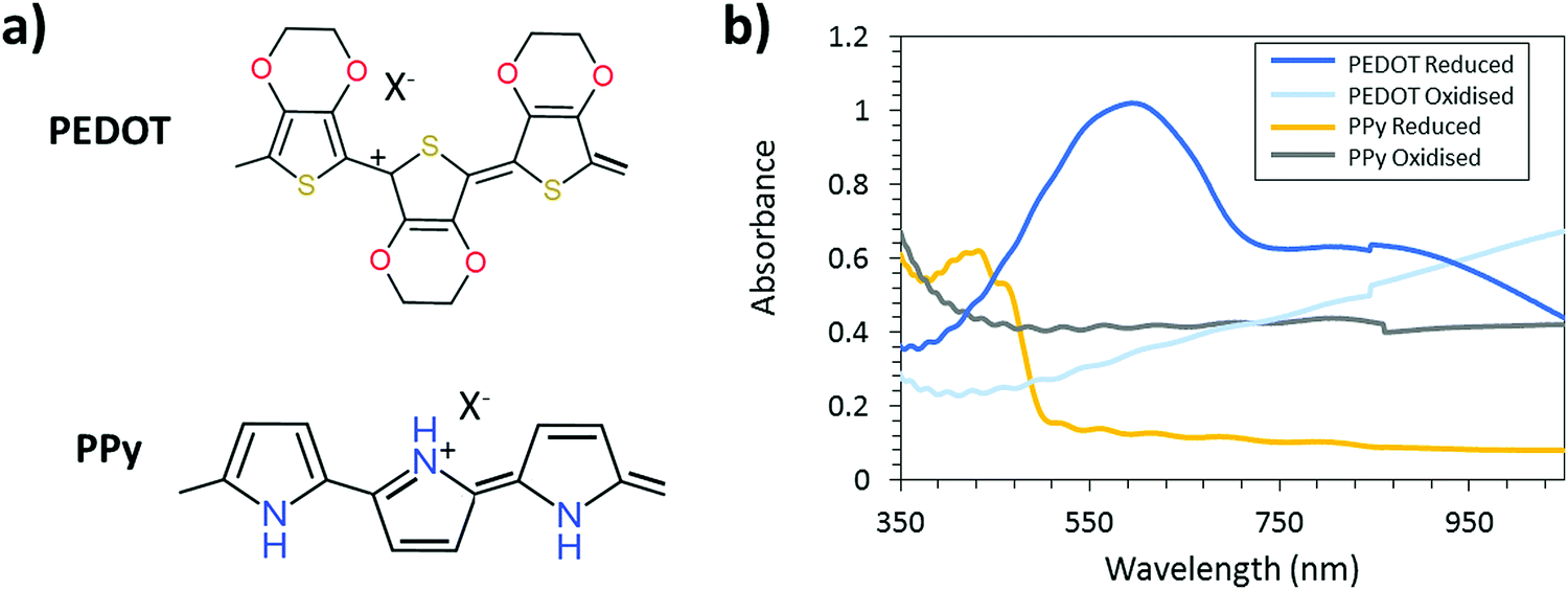 | ||
| Fig. 1 (a) Chemical structure of the oxidized state of PEDOT-X and PPy-X. (b) Absorption spectrum of the reduced and oxidized state of the CP. The most transparent film is for the reduced PPy and the most absorbing film is the reduced PEDOT. The combination of these CPs is suitable for smart window application due to their complementary nature. | ||
Herein we investigate the use of UV-light mediated patterning combined with VPP in order to produce high-resolution patterns of PEDOT and PPy with unique electrochromic properties to create an optoelectronic device switching between two images. In doing so, we have increased the versatility of the previously developed UV-light mediated patterning technique by showing that it is not limited to a specific CP. The process was first investigated for the CP PPy before the electrochromic resolution and contrast of both PEDOT and PPy patterns were analyzed and incorporated into prototype devices.
Experimental
CleviosTM CB 40 (40 wt% Fe(III) p-toluenesulfonate (Fe(Tos)3) in butanol) was purchased from Heraeus (Germany). 3,4-Ethylenedioxythiophene (EDOT), pyrrole, 1-ethyl-3-methylimidazolium ethyl sulfate (EMIM ES), hydroethyl cellulose (HEC) and triblock copolymer poly(ethylene glycol)-block-poly(propylene glycol)-block-poly(ethylene glycol) (PEG–PPG–PEG, 5800 g mol−1) were purchased from Sigma Aldrich. All chemicals were used as received without further purification.PPy thin films were synthesized similar to those reported previously.36 The oxidant solution was composed of Fe(Tos)3 (13.9 wt%) and PEG–PPG–PEG (13.0 wt%) in hexanol/butanol mix. Employing a higher boiling point solvent (hexanol) and a lower weight percentage of PEG–PPG–PEG, a surfactant used as polymerization inhibitor, resulted in stable films that did not dissolve during the washing step of the standard VPP procedure. The oxidant solution was spin coated onto glass substrates (with gold electrodes for electrical characterization), ITO-coated glass or plastic at 1500 rpm for 30 seconds. The oxidant coated substrates were placed on a 70 °C hot plate for 30 seconds before undergoing UV-light exposure for different time intervals using a UV-lamp with an intensity of 20 mW cm−2 at 405 nm and 10 mW cm−2 at 365 nm. For the patterning, photomasks were suspended above the oxidant coated substrates prior to UV-light exposure to create unexposed and exposed patterns. The oxidant was left to stand for 12 hours for crystallization observation studies only. Fabrication of high quality PPy was achieved by immediately polymerizing after UV-light exposure. Pyrrole VPP was performed at atmospheric pressure at room temperature for 60 minutes. After the polymerization, the thin films were washed with ethanol and air dried before analysis.
The procedure for the VPP of EDOT was similar to that previously reported23 where the oxidant solution was composed of Fe(Tos)3 (12.3 wt%) and PEG–PPG–PEG (23.1 wt%) in ethanol/butanol mix. The polymerization time was 30 minutes under vacuum conditions and a temperature of 60 °C.
Lateral electrochromic devices were constructed in order to examine the electrochromic properties of the individual PEDOT and PPy thin films. Thin films of PEDOT or PPy deposited on ITO-coated polyethylene terephthalate (PET) plastic were scratched in the middle to separate the electrodes. They were then incorporated into the devices using a gel electrolyte doctor bladed onto the films and then encapsulated with PET double sided adhesive with a PET top layer. The electrolyte used was EMIM ES with 7.5 wt% HEC as a gelling agent. Electrical input was applied in situ and the films experienced oxidization (1.5 V) and reduction (−1.5 V), and their ultraviolet-visible (UV-vis) spectra were acquired (Lambda 900 spectrometer, PerkinElmer). Spectra were recorded between 400–850 nm.
Prototype vertical electrochromic devices were constructed with the CPs deposited (and patterned) onto ITO-coated PET, with the CP counter electrode and ITO-coated PET electrode sandwiched between gel electrolytes and encapsulated with PET double sided adhesive. The electrochromic behaviour of the prototype devices was observed using an external power supply with the voltages ranging from 1.5 V to −1.5 V unless otherwise stated.
The modification of the electrochromic devices to permit two images within the one device required both CPs to be deposited onto a single ITO substrate. To achieve this, two UV-light mediated patterning VPP procedures were performed in sequence. A PPy pattern was synthesized first followed by a PEDOT pattern. The multilayer film was encapsulated with a bare ITO counter electrode, prioritizing the ability to observe the two images over longevity of the device. The PPy synthesis within the dual image device was altered by an increase in oxidant concentration (24 wt%) in order to increase the thickness of the layer and allow the image to become more visible.
Characterization
Color contrast measurements were performed on PEDOT and PPy samples in their oxidized and reduced states using a spectrophotometer (Datacolor Mercury). Two unexposed samples, one of PEDOT and one of PPy, were prepared on gold-coated glass substrates. These samples were larger in area than the ITO-coated substrates and acted as the counter electrodes during electrochemical switching. The larger area of the counter electrode ensures that enough charge can be supplied to the working electrode for a complete electrochemical switching to occur. The electrochemical switching was performed in 1 M KCl water solution while applying a voltage bias of ±1.5 V between the working and counter electrodes. The samples were switched between their oxidized and reduced states 5 times before performing the measurements. The samples were then switched to their oxidized/reduced state and dried with a nitrogen gun before performing the color measurements. The L*, a* and b* values were recorded and the color contrast, ΔE, was calculated from eqn (1):39| ΔE = [(L2* − L1*)2 + (a2* − a1*)2 + (b2* − b1*)2]1/2 | (1) |
Conductivity measurements were achieved using gold electrodes in a four-probe configuration patterned onto glass substrates using thermal evaporation. The area between the inner electrodes was 1 × 1 cm2. The sheet resistance (Rs) of the samples was measured using a source meter (Keithley 2400) in four-wire sense mode. The conductivity (σ) was calculated using the eqn (2):
 | (2) |
Film thickness and film morphology was obtained using atomic force microscopy (AFM). AFM images were obtained in tapping mode using a Veeco Dimension 3100. The morphological images and thickness measurements were analyzed using the WSxM 4.0 software.40 FTIR measurements were performed using an Equinox 55 spectrometer (Bruker). FTIR spectra were acquired in transmission mode using a resolution of 4 cm−1 and 64 scans. Spectra were baseline corrected. Undoped SiO2 wafers were employed as the substrate for measurements. A Nikon SMZ1500 microscope with a DS-Fi1 CCD sensor was used to acquire the magnified images.
Electrochemical measurements were performed using a three electrode setup on a AUTOLAB potentiostat (Metrohm) in 1 M aqueous KCl solution. Samples of PEDOT and PPy with different exposure times (0 s, 150 s, 300 s, 600 s and 900 s) were prepared on gold-coated glass substrates. A platinum counter electrode and an Ag/AgCl reference electrode were used. Galvanostatic discharge measurements were performed in the potential range 0–0.5 V at a constant current of 10 μA in order to calculate the film capacitance.
Results and discussion
Fig. 2(a) presents the UV-patterning technique to create high-resolution CP patterns. The oxidant, containing Fe(Tos)3 and PEG–PPG–PEG, is composed of a hexanol/butanol mix and deposited via spin-coating after which UV-light illuminates the oxidant film through a shadow mask. The vapor of pyrrole is exposed to the irradiated oxidant film within a closed chamber. The oxidant in the areas exposed to the UV-light is altered by the UV-light, so that the resultant PPy has modified optical and electrical properties. As seen previously for UV-light mediated patterned VPP PEDOT, lines widths of 10 μm can be created using this patterning technique.34Fig. 2(b) presents patterned lines of PPy with exposed (900 seconds) and unexposed areas with the smallest line being 10 μm with further images shown in Fig. S1 (ESI†). PPy patterned lines, together with atomic force microscopy images displaying topography of the exposed and unexposed regions can be seen in Fig. S2 (ESI†). Both regions exhibit grain-like structure at the nanometer scale, yet the micrometer morphology shows distinct differences, with the exposed regions possessing large crystal-like structures.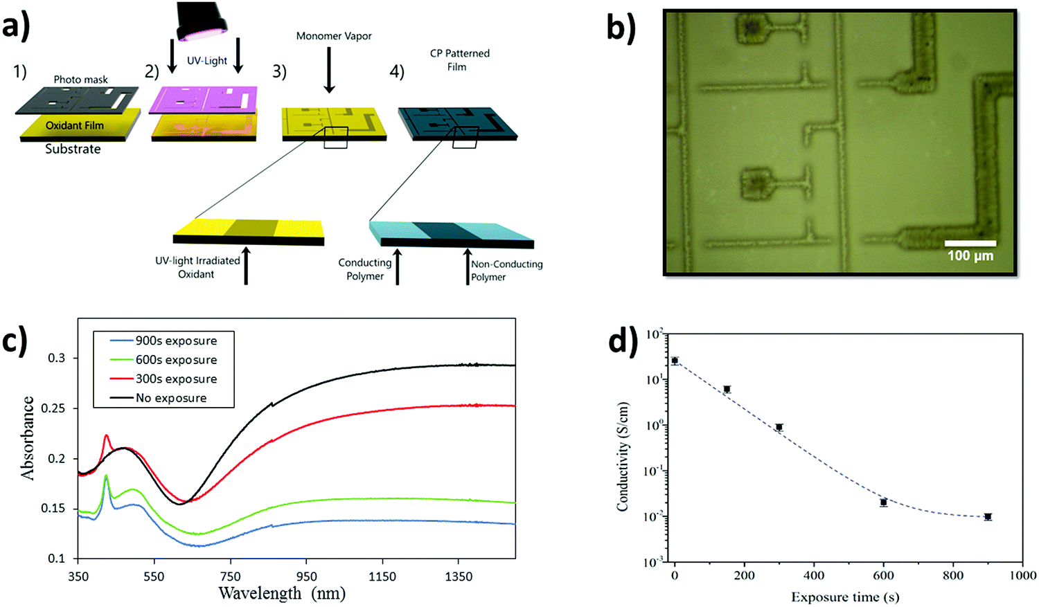 | ||
| Fig. 2 (a) Schematic of the UV-patterning technique (1) deposition of an oxidant solution, (2) exposure to UV-light through a photo mask, (3) polymerization of the monomer species via VPP, (4) post washing procedure resulting in a patterned CP thin film. Insets show that poorly CP results from the oxidant regions irradiated with UV-light. (b) High-resolution patterning of PPy producing conductive and non-conductive regions with line widths of the order of 10 μm. (c) UV-Vis absorption spectra and (d) conductivity measurements of PPy thin films after the oxidant was exposed to UV-light for various times before vapor phase polymerization of pyrrole was performed. | ||
A range of PPy films were fabricated using varying amounts of UV-light exposure of the oxidant prior to the VPP step. The optical properties of the obtained PPy films were altered due to the UV-light treatment, as reported previously for PEDOT.34 The UV-vis spectra in Fig. 2(c) show a general trend of lower absorption in the near IR region for increased exposure time. This decrease in absorption corresponds to a reduction in bipolaron formation41,42 also supported by the reduction in conductivity measured for films obtained with increasing exposure times (Fig. 2(d)). The appearance of a sharp peak at 425 nm in the UV-vis has been reported also for PEDOT films obtained after UV-light exposure,34 and is believed to originate from shortened polymeric chains.43 The peak appears to grow in strength with exposure time, indicating that increased UV-light exposure may create a larger amount of shorter polymer chains resulting from an increase in nucleation sites. The hypothesis of nucleation sites is supported by the observation of the crystallites formed in the oxidant (allowed to stand for 12 hours to be observable) as in Fig. S3 (ESI†). Increased crystallization impacts the final PPy thin films as the polymerization adopts the same morphology present in the oxidant. Evidence of the oxidant ‘guiding’ the polymer morphology can be found in Fig. S4 (ESI†). PPy was synthesized with the oxidant left to stand for 12 hours and the CP adopts exactly the same morphology trends found within the oxidant samples (all further PPy films were synthesized immediately after exposure).
FTIR analysis was conducted on PPy thin films in order to support the conductivity measurements and observe any additional changes within the films following the UV-light treatment. The main modification that was observed in the FTIR features of PPy thin films (Fig. S5, ESI†) is the reduction of the peak at 1510 cm−1 and the reduction in the overall absorption from 1500 to 3500 cm−1. The peak at 1510 cm−1 relates to C![[double bond, length as m-dash]](https://www.rsc.org/images/entities/char_e001.gif) C stretching and the broad band at higher wavenumbers (1500 to 3500 cm−1) has been previously reported to be associated with the oxidation level of CPs and the transition from bipolarons to polarons (refer to summary in ESI†).44 Therefore, the reduction in both these peaks suggests the CP is both changing doping state and conjugation length, thus corroborating the UV-vis and the conductivity measurements.
C stretching and the broad band at higher wavenumbers (1500 to 3500 cm−1) has been previously reported to be associated with the oxidation level of CPs and the transition from bipolarons to polarons (refer to summary in ESI†).44 Therefore, the reduction in both these peaks suggests the CP is both changing doping state and conjugation length, thus corroborating the UV-vis and the conductivity measurements.
In our previous report,34 long exposure times of the oxidant solution followed by EDOT VPP resulted in degradation or removal of the polymeric material upon washing the samples. This was not observed with PPy formation. The exposed regions of the PPy thin films remained after the washing step even after long exposure periods (900 seconds). The fast polymerization of pyrrole is thought to create PPy capable of withstanding the washing procedure. The faster polymerization of pyrrole through VPP has been well documented previously.16,45 It is believed there is sufficient PPy formed to become entangled and therefore to remain intact during the washing step, however, this is yet to be proven. Regardless of why the PPy remains, complex patterns of PPy possessing regions of high and low conductivity can be created with examples such as circuits and advertising logos as shown in Fig. S1 (ESI†). However, the electrochromic potential of these high-resolution patterns and images has yet to be exploited.
Fig. S6 (ESI†) presents the electrochromic behaviour of the PPy thin films fabricated after the oxidant was exposed to UV-light for various time periods. The difference in absorbance intensities between the oxidised and reduced states of PPy was shown to decrease with increasing exposure times in both the visible and near-IR regions, resulting in a reduction in visible contrast. Similar reductions in colour contrast over the visible spectrum are observed for PEDOT samples after the oxidant is exposed to UV-light for increasing time periods (Fig. S7, ESI†). However, in addition to a decrease in contrast, the reduced state of the exposed PEDOT appears purple instead of the characteristic dark blue. The colour contrast of the individual films was further analysed using a handheld spectrophotometer with the contrast calculation based on the L*a*b* colour space coordinates in order to quantitatively evaluate the difference in the contrast. Fig. 3(a) displays the trend of colour contrast between reduced and oxidized states, with increasing UV-light exposure times of the oxidant.
 | ||
| Fig. 3 (a) Color contrast values of PEDOT (black) and PPy (blue) calculated by L*a*b* color space of the oxidized and reduced states of films following various UV-light exposure times. (b) Color contrast differences between oxidized and reduced states of the unexposed and exposed CPs. The contrast values are the exposed samples compared to the unexposed values. E.g. PEDOT exposed for 900 s in the reduced state was compared to the unexposed reduced PEDOT to give a contrast value of over 35. (c) Electrochromic patterns of PEDOT and PPy after the oxidant was exposed for 900 s in their oxidized and reduced states. 100 μm lined patterns are visible in the PEDOT film in the reduced state while the pattern in the PPy thin film is visible in the oxidized state. | ||
The color contrast between the exposed and unexposed regions for both PEDOT and PPy at different exposure times is shown in Fig. 3(b). The graph presents both CPs in their reduced and oxidized states and compares them to the unexposed CPs. The contrast values are therefore the contrast between the oxidized state of the exposed samples and the oxidized state of the unexposed sample. From this graph it is clear that the contrast between a pattern and its surrounding (regions exposed to UV-light) increases with increasing exposure time. It also shows the greatest contrast is shown in the reduced PEDOT state confirming the UV-light effect is more dominant on the reduction redox state in PEDOT. PPy however, shows a more even effect on both oxidized and reduced states albeit lower contrasts to the unexposed sample.
PEDOT and PPy patterning via the UV-light mediated technique accomplishes the significant goal of combining micro and macro patterning using the same patterning procedure. Electrochromic behavior in patterned CPs has been sparsely reported within the scientific literature24 and not at all for the micrometer scale. UV-Light mediated patterning of the oxidant solution prior to VPP allows CP patterns with micrometer resolution and nanometer thickness for electrochromic applications. Not only can the patterns be fabricated quickly and of various sizes (the deposition of oxidant being the only practical limitation), the resolution of the patterns is retained in its electrochromic behavior, with the change in optical properties having a definite micrometric edge. The electrochromic resolution of 100 μm can be observed in Fig. 3(c) with both PEDOT and PPy displaying electrochromic patterns appearing and disappearing depending on the applied voltage.
The exposed regions of the PEDOT and PPy shown throughout this report are not as electroactive as the unexposed regions as demonstrated by a reduction in electrochromic contrast between oxidized and reduced states. It may be argued that the reduction in electroactivity is due to a reduction in the CPs ability to accommodate charges, as demonstrated by the lower charge carrier concentrations in FTIR measurements. In an electrochromic cell, charge transfer reactions occur at both electrodes and the charges on one electrode must always balance those on the other. For a complete electrochromic reaction to occur, the counter electrode must therefore have high enough charge storage capacity. It is therefore important to investigate how the capacitance of the CPs change during the UV-VPP process. Fig. S8 (ESI†) shows how the capacitance changes with increasing UV-light exposure. Both for PEDOT and PPy the capacitance decreases at high exposures by ∼25% in the case of PEDOT and 75% in the case of PPy. The reduced capacitance could have consequences in devices where both electrodes are required to undergo an electrochromic reaction. If there is a large UV-light exposed area on one electrode, then it might not have large enough capacitance to balance the opposite electrode. However, since capacitance increases with film thickness, this can easily be compensated for by producing thicker CP films on the patterned electrode.
Fig. 4(a) presents a simple device architecture incorporating a patterned PEDOT (900 s exposure) film and a PEDOT counter electrode both deposited on ITO-coated PET. As shown in Fig. 3(b) the color contrast between exposed and unexposed regions of PEDOT is greater in their reduced states than in their oxidized states. This has the effect that a pattern will be more visible in one state than the other, and switching between the two states will make the pattern appear and disappear, aided in this by the dark color of the back electrode in its reduced state. A movie of the working prototype is presented in ESI,† Movie 1. The color contrast is less intense for PPy as mentioned previously and shown in Fig. 3(b). However, Fig. 4(b) displays an electrochromic device incorporating patterned PPy albeit employing a white electrolyte that is opaque instead of transparent which highlights the advertising application of PPy patterns. A prototype device employing the transparent gel electrolyte and two PPy layers can be seen in Fig. S9 (ESI†). Despite the lower contrast, the images are still visible in the oxidized state yet disappear in the PPy reduced state. We observe that the visibility of the PPy pattern is enhanced using the opaque electrolyte compared to the transparent electrolyte, but the opposite is true for the PEDOT pattern (more visible as a window with back lighting). An explanation to this is still under investigation. By combining both CPs together with a transparent electrolyte, a smart window device including a pattern visible with moderate contrast can be achieved – an example of this is shown in Fig. S10 (ESI†) and a conceptual application demonstrated in Fig. S11 (ESI†).
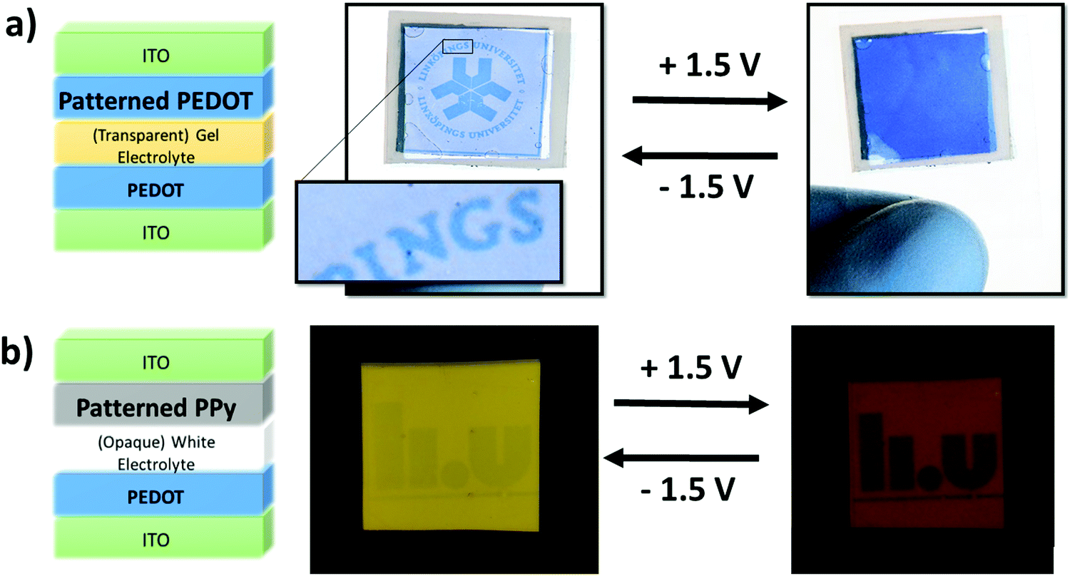 | ||
| Fig. 4 Prototype patterned electrochromic devices. (a) PEDOT electrochromic device design incorporating a UV-light patterned PEDOT layer with PEDOT as the counter polymer. The device is shown in both states where the university logo becomes visible during reduction of the patterned PEDOT and disappears during oxidation with the aid of the counter PEDOT's dark reduced state. (b) Electrochromic device design incorporating a UV-light patterned PPy layer with PPy as the counter polymer. The PPy device in both states is presented with the pattern becoming visible when the patterned PPy layer is oxidized and disappears when the it is reduced. *Voltages stated are applied to the patterned CPs. | ||
As shown throughout this report, the patterns within the CP films effectively appear and disappear with the applied voltage. Therefore, one can reasonably assume that two images can be incorporated into a single electrochromic device through the incorporation of two patterned CP film. To achieve a dual image electrochromic device, we combined a patterned PEDOT and patterned PPy layer on top of each other.
The fact that images imprinted into the PEDOT and PPy films via UV-patterning are complementary to each other (PEDOT patterns visible when reduced and PPy patterns visible when oxidized) does not allow for two images to be shown in a singular electrochromic device in the previous device architecture. If both, patterned PEDOT and patterned PPy were included in the device architecture shown previously, the patterns would overlap with neither image appearing individually. However, if the current electrochromic device architecture is modified two images can appear within a singular device. In order to achieve this goal the patterned PEDOT and PPy must be deposited onto the same ITO electrode. PPy was deposited first due to its fragility followed by PEDOT. There appeared to be no adverse effects of the UV-light on the patterned PPy film or any difficultly patterning a PEDOT film on PPy aside from some minor defects originating from spin coating. Fig. 5(a) shows the new electrochromic device architecture to produce multiple images within a single device while Fig. 5(b) illustrates the individual electrochromic behavior of both patterned CPs when they are under an applied bias. Unfortunately, due to the electrochromic device architecture, the switching speed was slow (5 minutes) and the lifetime is limited and needs to be improved.
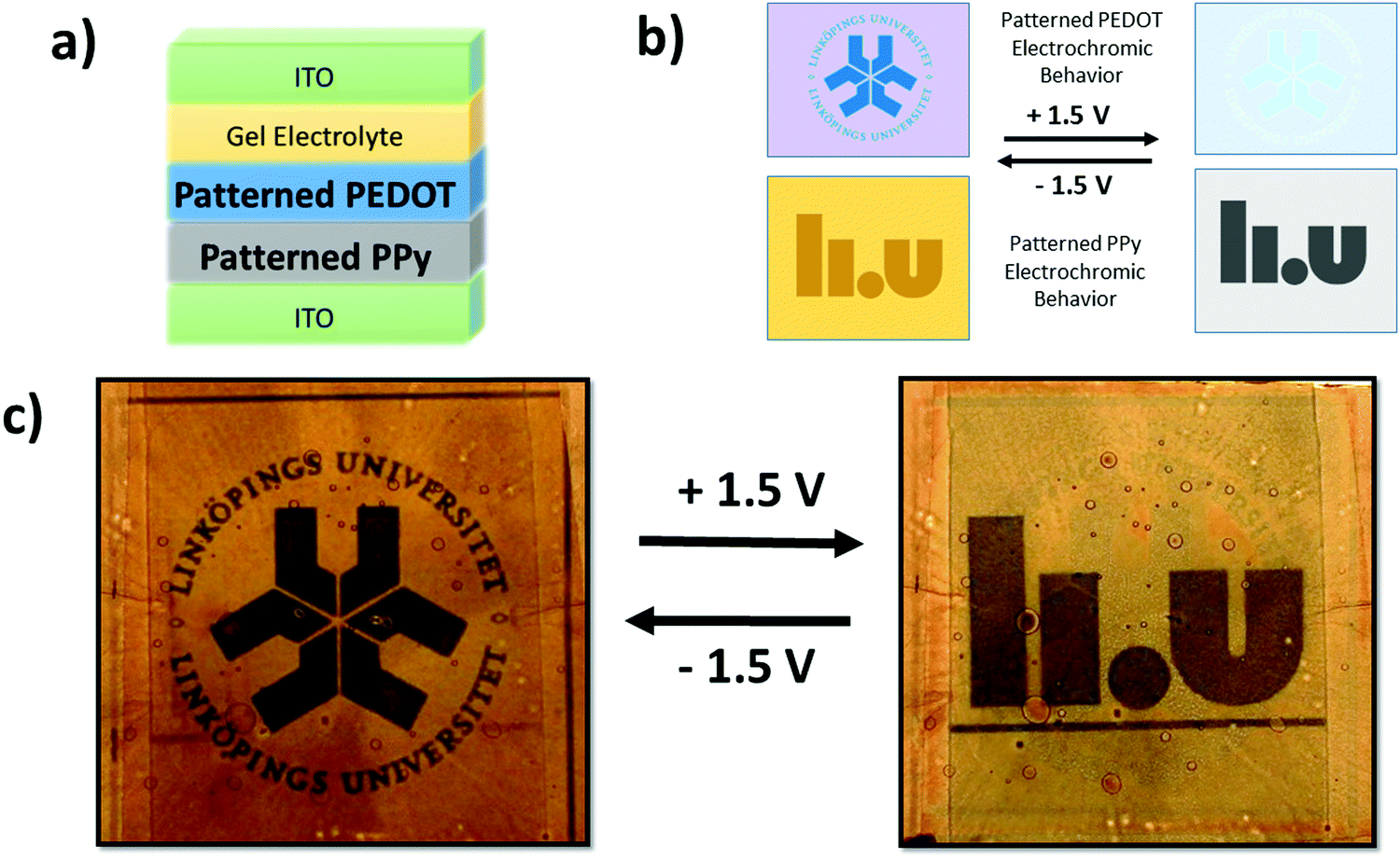 | ||
| Fig. 5 (a) Dual image electrochromic device architecture showing the change in structure with both CPs deposited onto one ITO substrate. (b) Individual electrochromic behaviour schematic of the two patterned CPs when under applied voltages of +1.5 V and −1.5 V. The images appear and disappear in opposites allowing a double image device. (c) Dual image electrochromic device in both states showing clearly both individual images. | ||
The schematic shows that when the PEDOT pattern is oxidized, it exhibits similar optical properties to the surrounding exposed PEDOT and disappears, while the PPy pattern is dissimilar in optical properties when oxidized and becomes more visible. The opposite is observed when the CPs are reduced with the PEDOT pattern being observed while the PPy image disappears. Thus, the manipulation of the device architecture and the materials results in an electrochromic device exhibiting two different images – one when oxidized and the other when reduced. Fig. 5(c) presents the final multiple image electrochromic device in its reduced and oxidized forms clearly displaying the two different Linköping University logos.
Conclusion
We have demonstrated that a newly developed UV-light patterning technique can be adapted to accommodate CPs other than PEDOT, such as PPy, with similar effects on the resultant CP film. We further showed that the electrochromic contrast between two redox states can be tuned using UV-light exposure. A reduction of conductivity was observed with increasing UV-light exposure time which was shown using UV-vis, FTIR and electrical measurements. Complex patterns of PPy with high-resolution were achieved by exploiting photomasks during the UV-light exposure. The micron-scale resolution patterns (100 μm) created by treating the oxidant with UV-light were shown to retain their electrochromic behavior. The patterns possessed similar optical properties in one redox state and dissimilar properties in the other resulting in high resolution patterns that disappeared and appeared with the change in applied electrical bias. This electrochromic property is unique to the UV-VPP patterning technique and was observed for both PPy and PEDOT albeit in opposite states (patterns visible in the oxidized state for PPy and the reduced state for PEDOT) and displayed in prototype electrochromic devices. A new type of electrochromic device capable of switching between two patterns was realized using a new electrochromic device architecture. This type of dual image device has not been previously reported in the field of electrochromics and could potentially be used in various optoelectronic device applications such as displays, smart windows, and adaptive IR camouflaging.Author contributions
R. B. and J. E. performed the experiments, designed the devices and wrote the manuscript. D. I. helped with the design of experiments and worked on the editing of the manuscript. M. B., X. C. and I. E. co-supervised the project and contributed to the editing of the manuscript.Conflicts of interest
The authors declare that they have no competing interests.Acknowledgements
The authors acknowledge by the Knut and Alice Wallenberg foundation KAW (Tail of the Sun, KAW 2014.0041 and Power Papers, KAW 2011.0050) and the Swedish Foundation for Strategic Research (Synergy project), XC is financed by the European Research Council (ERC-starting-grant 307596), and the Advanced Functional Materials Center at Linköping University. The authors would like to thank Dr Eliot Gomez and Dr Daniel Tordera for the photography and videography of the electrochromic devices.References
- K. Doblhofer, Soft Mater., 2008, 6, 156 CrossRef.
- D. R. Rosseinsky and R. J. Mortimer, Adv. Mater., 2001, 13, 783–793 CrossRef CAS.
- J. Kawahara, P. A. Ersman, I. Engquist and M. Berggren, Org. Electron., 2012, 13, 469–474 CrossRef CAS.
- R. Brooke, E. Mitraka, S. Sardar, M. Sandberg, A. Sawatdee, M. Berggren, X. Crispin and M. P. Jonsson, J. Mater. Chem. C, 2017, 5, 5824–5830 RSC.
- C. Louet, S. Cantin, J.-P. Dudon, P.-H. Aubert, F. Vidal and C. Chevrot, Sol. Energy Mater. Sol. Cells, 2015, 143, 141–151 CrossRef CAS.
- P. R. Somani and S. Radhakrishnan, Mater. Chem. Phys., 2003, 77, 117–133 CrossRef CAS.
- C. M. Lampert, Sol. Energy Mater., 1984, 11, 1–27 CrossRef CAS.
- D. M. DeLongchamp and P. T. Hammond, Chem. Mater., 2004, 16, 4799–4805 CrossRef CAS.
- A. Malti, R. Brooke, X. Liu, D. Zhao, P. Andersson Ersman, M. Fahlman, M. P. Jonsson, M. Berggren and X. Crispin, J. Mater. Chem. C, 2016, 4, 9680–9686 RSC.
- A. A. Argun, P.-H. Aubert, B. C. Thompson, I. Schwendeman, C. L. Gaupp, J. Hwang, N. J. Pinto, D. B. Tanner, A. G. MacDiarmid and J. R. Reynolds, Chem. Mater., 2004, 16, 4401–4412 CrossRef CAS.
- Y. Cao, A. Andreatta, A. J. Heeger and P. Smith, Polymer, 1989, 30, 2305–2311 CrossRef CAS.
- D. Kumar and R. C. Sharma, Eur. Polym. J., 1998, 34, 1053–1060 CrossRef CAS.
- R. Balint, N. J. Cassidy and S. H. Cartmell, Acta Biomater., 2014, 10, 2341–2353 CrossRef CAS PubMed.
- T. Moser, C. Celma, A. Lebert, E. Charrault, R. Brooke, P. J. Murphy, G. Browne, R. Young, T. Higgs and D. Evans, ACS Appl. Mater. Interfaces, 2016, 8, 974–982 CAS.
- R. Brooke, P. Cottis, P. Talemi, M. Fabretto, P. Murphy and D. Evans, Prog. Mater. Sci., 2017, 86, 127–146 CrossRef CAS.
- B. Winther-Jensen, J. Chen, K. West and G. Wallace, Macromolecules, 2004, 37, 5930–5935 CrossRef CAS.
- B. Winther-Jensen and F. C. Krebs, Sol. Energy Mater. Sol. Cells, 2006, 90, 123–132 CrossRef CAS.
- C. Xu, P. Wang and X. Bi, J. Appl. Polym. Sci., 1995, 58, 2155–2159 CrossRef CAS.
- M. Fabretto, K. Zuber, C. Hall and P. Murphy, Macromol. Rapid Commun., 2008, 29, 1403–1409 CrossRef CAS.
- N. Vucaj, M. D. J. Quinn, C. Baechler, S. M. Notley, P. Cottis, P. Hojati-Talemi, M. V. Fabretto, G. G. Wallace, P. J. Murphy and D. R. Evans, Chem. Mater., 2014, 26, 4207–4213 CrossRef CAS.
- B. Winther-Jensen and K. West, Macromolecules, 2004, 37, 4538–4543 CrossRef CAS.
- O. Bubnova, Z. U. Khan, H. Wang, S. Braun, D. R. Evans, M. Fabretto, P. Hojati-Talemi, D. Dagnelund, J.-B. Arlin, Y. H. Geerts, S. Desbief, D. W. Breiby, J. W. Andreasen, R. Lazzaroni, W. M. Chen, I. Zozoulenko, M. Fahlman, P. J. Murphy, M. Berggren and X. Crispin, Nat. Mater., 2014, 13, 190–194 CrossRef CAS PubMed.
- M. V. Fabretto, D. R. Evans, M. Mueller, K. Zuber, P. Hojati-Talemi, R. D. Short, G. G. Wallace and P. J. Murphy, Chem. Mater., 2012, 24, 3998–4003 CrossRef CAS.
- R. Brooke, D. Evans, M. Dienel, P. Hojati-Talemi, P. Murphy and M. Fabretto, J. Mater. Chem. C, 2013, 1, 3353–3358 RSC.
- S. Holdcroft, Adv. Mater., 2001, 13, 1753–1765 CrossRef CAS.
- Y. Xu, F. Zhang and X. Feng, Small, 2011, 7, 1338–1360 CrossRef CAS PubMed.
- H.-S. Liu, W.-C. Chang, C.-Y. Chou, B.-C. Pan, Y.-S. Chou, G.-S. Liou and C.-L. Liu, Sci. Rep., 2017, 7, 11982 CrossRef PubMed.
- A. Kumar, S.-Y. Jang, J. Padilla, T. F. Otero and G. A. Sotzing, Polymer, 2008, 49, 3686–3692 CrossRef CAS.
- J. Jensen, A. L. Dyer, D. E. Shen, F. C. Krebs and J. R. Reynolds, Adv. Funct. Mater., 2013, 23, 3728–3737 CrossRef CAS.
- P.-H. Aubert, A. A. Argun, A. Cirpan, D. B. Tanner and J. R. Reynolds, Chem. Mater., 2004, 16, 2386–2393 CrossRef CAS.
- C. B. Nielsen, A. Angerhofer, K. A. Abboud and J. R. Reynolds, J. Am. Chem. Soc., 2008, 130, 9734–9746 CrossRef CAS PubMed.
- M. A. Invernale, Y. Ding and G. A. Sotzing, ACS Appl. Mater. Interfaces, 2010, 2, 296–300 CAS.
- Y. Ding, M. A. Invernale and G. A. Sotzing, ACS Appl. Mater. Interfaces, 2010, 2, 1588–1593 CAS.
- J. Edberg, D. Iandolo, R. Brooke, X. Liu, C. Musumeci, J. W. Andreasen, D. T. Simon, D. Evans, I. Engquist and M. Berggren, Adv. Funct. Mater., 2016, 26, 6950–6960 CrossRef CAS.
- O. Winther-Jensen, S. Desai, R. L. Shepherd, P. C. Innis, B. Winther-Jensen, M. Forsyth, G. G. Wallace and D. R. MacFarlane, Electrochem. Commun., 2010, 12, 1505–1508 CrossRef CAS.
- R. Brooke, M. Fabretto, N. Vucaj, K. Zuber, E. Switalska, L. Reeks, P. Murphy and D. Evans, Smart Mater. Struct., 2015, 24, 035016 CrossRef.
- L. Jiang, H.-K. Jun, Y.-S. Hoh, J.-O. Lim, D.-D. Lee and J.-S. Huh, Sens. Actuators, B, 2005, 105, 132–137 CrossRef CAS.
- A. Ramanavičius, A. Ramanavičienė and A. Malinauskas, Electrochim. Acta, 2006, 51, 6025–6037 CrossRef.
- J. Kawahara, P. A. Ersman, I. Engquist and M. Berggren, Org. Electron., 2012, 13, 469–474 CrossRef CAS.
- I. Horcas, R. Fernández, J. M. Gómez-Rodríguez, J. Colchero, J. Gómez-Herrero and A. M. Baro, Rev. Sci. Instrum., 2007, 78, 013705 CrossRef CAS PubMed.
- Z. U. Khan, O. Bubnova, M. J. Jafari, R. Brooke, X. Liu, R. Gabrielsson, T. Ederth, D. R. Evans, J. W. Andreasen, M. Fahlman and X. Crispin, J. Mater. Chem. C, 2015, 3, 10616–10623 RSC.
- E. Spain, T. E. Keyes and R. J. Forster, Biosens. Bioelectron., 2013, 41, 65–70 CrossRef CAS PubMed.
- O. Bubnova, Z. U. Khan, A. Malti, S. Braun, M. Fahlman, M. Berggren and X. Crispin, Nat. Mater., 2011, 10, 429–433 CrossRef CAS PubMed.
- C. Kvarnström, H. Neugebauer, A. Ivaska and N. S. Sariciftci, J. Mol. Struct., 2000, 521, 271–277 CrossRef.
- P. Subramanian, N. Clark, B. Winther-Jensen, C. Douglas Macfarlane and L. Spiccia, Aust. J. Chem., 2009, 62, 133–139 CrossRef CAS.
Footnote |
| † Electronic supplementary information (ESI) available. See DOI: 10.1039/c7tc05833k |
| This journal is © The Royal Society of Chemistry 2018 |