Tunable dipole and carrier mobility for a few layer Janus MoSSe structure†
Abstract
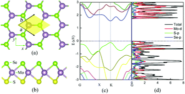
Transition metal chalcogenides have attracted considerable attention for the further development of nanoscale devices, however low carrier mobility seriously prevents its further application. Here, the first-principles calculations are used to explore the structural, electronic, and carrier mobility properties of few layer Janus MoSSe in different types of stacking. The result shows that AC-stacking is the most favored stacking regardless of combination mode. Besides the band gap regulation, the dipole moment perpendicular to the x–y plane can be effectively modified through varying of the combination mode and thickness of few layers, which is further evidenced by the plane electrostatic potential energy difference between the two sides. Furthermore, the carrier mobility in these Janus structures can be greatly affected by the dipole and thickness. Although the carrier mobility in monolayer MoSSe is relatively low, the bilayer or trilayer structures have a quite high electron carrier mobility of 1194 cm2 V−1 s−1 and hole carrier mobility of 5894 cm2 V−1 s−1, mainly determined by the deformation potential. The results presented here show that the few layer Janus MoSSe has a potential in designing electronic devices or photocatalysts such as for water splitting with the intrinsic built-in electronic field.


 Please wait while we load your content...