
 Open Access Article
 This Open Access Article is licensed under a
 Creative Commons Attribution 3.0 Unported Licence
Electrochromic bilayers of Prussian blue and its Cr analogue†
Luke
Hedley
 a,
Liz
Porteous
b,
David
Hutson
b,
Neil
Robertson
a and
J. Olof
Johansson
*a
a,
Liz
Porteous
b,
David
Hutson
b,
Neil
Robertson
a and
J. Olof
Johansson
*a
aEaStCHEM, School of Chemistry, University of Edinburgh, David Brewster Road, EH9 3FJ, UK. E-mail: olof.johansson@ed.ac.uk
bSchool of Engineering and Computing, University of the West of Scotland, Paisley PA1 2BE, UK
First published on 6th December 2017
Abstract
Multilayered thin films of functional materials play an important role in many applications in nanotechnology. The intense and tuneable colours of some molecular materials allow for the development of a unique spectral fingerprint of each layer in thin film heterostructures. Herein, we report on electrochromic switching of bilayer thin films composed of Prussian blue (FeIIIFeII) and its orange-coloured (FeIICrIII) analogue. The films could be switched from green to orange by reducing the blue FeFe top layer. The distinct optical absorption spectra of the two layers allowed spectroelectrochemical measurements to probe the electrochemical activity of the individual layers during the switching of the Prussian blue layer. We found that for producing layers of equal optical density, the thickness of the layers had to be different due to a difference in oscillator strength for the metal-to-metal charge-transfer transition. The films used here had a thickness of 300 ± 70 nm and 30 ± 15 nm for the FeCr and FeFe sub-layers, respectively. The colouration efficiency was found to be 147.8 ± 0.8 cm2 C−1 for the multilayered film. These results show that it is possible to obtain bilayers of Prussian blues that, with a unique optical spectral fingerprint of each sub-layer, retain the electrochromic functionality and therefore enable layer-sensitive studies of charge-transfer processes in thin film heterostructures of multifunctional materials.
Introduction
Multilayered thin films and heterostructures are ubiquitous to a wide range of areas such as solar cells and spintronics. They can be used as smart materials because at the interface of nanoscale heterostructures, new phenomena can arise due to the large surface-to-volume ratio. However, it can be difficult to study charge-transfer and other processes of individual layers in multilayers and so a probe that is sensitive to all layers is desirable. Molecular-based materials that display strong optical charge-transfer transitions can often be modified to tune their absorption spectrum. Carefully choosing the layers such that each layer has a distinct optical spectrum, allows for obtaining a handle on each sub-layer in order to study charge transfer processes across interfaces in multilayers. In particular, electrochromic properties provide a visually pleasing example of achieving electrical control of the colour of the materials and to study the change in absorption spectrum after a redox process. Multilayers containing electrochromic components can be used in multi-coloured electrochromic devices, for applications in smart windows and displays.1,2One of the most studied electrochromic materials is Prussian blue (PB), which can be switched from blue to transparent upon reduction. PB and its analogues are coordination polymers comprising transition metal ions linked by cyanide ligands in a rock-salt structure. A wealth of heterostructures exist which contain PB in combination with other materials, such as dye-sensitised titania3 and conductive polymers.4,5 There have also been a number of studies that employ multiple Prussian blue analogues (PBAs) to create heterostructures in the form of thin films or nanoparticles to study photo-induced magnetism6,7 and magneto-structural effects.8–10 Their electrochemical11 and optical12 properties have also been studied. In particular, Liao et al.12 made a PB and NiFe PBA composite material using a conductive polymer matrix, which exhibited electrochromic switching. To date, layer-by-layer deposition has been the most common way of making heterostructures of PBAs due to the high degree of control of layer thickness this method allows, which is critical in applications such as ion sieving,13,14 biosensing15 and for the synthesis of electrochromic materials.16 Notably, a sequential electrochemical approach was recently used by Prieto-Ruiz et al.9 to combine two magnetically ordered analogues of PB.
The strong colour of some PBAs, and indeed PB itself, arises due to metal-to-metal charge-transfer (MMCT) transitions, which can be tuned by varying the transition metals and the stoichiometry of the films.17,18 In this paper, we have tested the possibility to fabricate multilayers of PBAs in order to provide a structure with distinct optical spectra for each layer. We have successfully deposited the FeFe PB (blue) on top of the FeCr PBA (orange) using successive electrochemical depositions. The resulting overall colour of the film was green. By applying alternating electrical potentials, we are able to selectively reduce and oxidise the FeFe layer resulting in an overall reversible colour change from green to orange due to the electrochromic properties of PB. By using the unique optical spectra as a handle on each of the sub-layers in the material we were able to observe the electrochromic switching of the FeFe layer as part of a FeFe–FeCr multilayered structure. These measurements open up the possibility to control the optical properties of multilayered functional materials and the layer-sensitivity enables ground-breaking studies of charge-transfer processes in important multilayers and heterostructures with applications for solar cells, spintronics and photonic devices.
Experimental
Electrochemistry
As a working electrode, 1 mm thick glass (aluminoborosilicate) substrates coated with a conductive fluorine-doped tin oxide (FTO) layer were used, with a sheet resistance of 8 Ω sq−1. The substrates were cut to size (8 × 25 mm) and subsequently cleaned in water/detergent solution in an ultrasonic bath for 20 min. The process was repeated with isopropanol and methanol separately, rinsing with the previous solvent after each step to remove impurities on the surface. The cleaned substrates were then dried under a stream of nitrogen gas.The electrochemical experiments were carried out using a Metrohm-Autolab μAUTOLAB III potentiostat with a saturated calomel reference electrode (SCE) and a Pt counter electrode used for the electrochemical depositions. For the FeCr deposition, concentrations of 37.5 and 25 mM of FeCl3 and K3[Cr(CN)6] were used, respectively. For the subsequent FeFe deposition, a concentration of 7.5 mM was used for both the K3[Fe(CN)6] and the FeCl3. For all results presented here, 1 M of KCl(aq) was used as an electrolyte. From previous work, it is known that a more negative voltage is needed to produce FeCr (around −0.5 V9,19), than to deposit the FeFe PB (around 0.2 V vs. Ag/AgCl,20 although this varies slightly as the FeFe PB is best deposited with a constant current). The order in which the layers are deposited is important to avoid any substantial electrochemical modification of the first layer during the electrodeposition of the second layer. Therefore, deposition of the FeCr PBA was carried out first, using FeCl3 and K3[Cr(CN)6], potentiostatically at −0.7 V based on the work of Ohkoshi et al.18 At this potential, solvated Fe3+ ions are reduced to Fe2+ at the surface of the electrode. This reduced cation subsequently binds to the hexacyanochromate anion to form the insoluble PBA directly on the substrate.
For FeFe deposition, the electrochemical cell is filled with FeCl3 and K3[Fe(CN)6]3− along with the electrolyte. The FeCr film is used as an electrode in order to reduce the [Fe(CN)6]3− ions in solution to [Fe(CN)6]4−, which subsequently reacts with Fe3+ cations at the electrode surface. The product is the insoluble PB created on the FeCr electrode surface. In contrast to FeCr, where a potentiostatic deposition resulted in the optically clearest films, the PB films were deposited galvanostatically at −40 μA. This was previously found to yield the most homogeneous films,21 which we also observed. After deposition, the films were thoroughly rinsed with distilled water and subsequently dried under continuous N2 flow.
The spectroelectrochemical measurements were carried out using a halogen light source (Ocean Optics HL-2000-FHSA) which was coupled to a spectrometer (Ocean Optics HR2000+) through optical fibres. These optical fibres could be coupled to a cuvette holder where a 10 × 10 mm cuvette was used as the electrochemical cell. In order to fit all the required electrodes for the spectroelectrochemical measurements into the cuvette, the SCE reference and counter electrode were replaced with Pt wire electrodes. A previous investigation22 of this arrangement of electrodes showed that the use of the pseudo-reference results in a shift of less than 0.02 V with respect to the SCE arrangement. Cyclic voltammograms were carried out on each of the layers individually and the bilayer structure in order to determine switching potentials to be used during the spectroelectrochemistry.
Characterisation
Optical transmission spectra were recorded using a Shimadzu UV-1800 UV Spectrophotometer. IR spectra were collected using a Renishaw InVia Raman Microscope equipped with a reflection FTIR instrument. We found that the reflectivity of the FTO layer allowed for more sensitive IR measurements of the thin films than using an attenuated total reflectance instrument. Information on the thickness and crystal formation was gathered using various techniques. Atomic force microscopy (AFM) was used to measure the thicknesses of the films. The samples were prepared for AFM measurements using a razor blade drawn across the film in order to remove material from the electrode. This produces a ‘valley’ in the film which can be studied using the AFM tip. Several cross sections were taken in order to reliably assess the step height (Fig. S1, ESI†). Scanning electron microscopy (SEM) and energy dispersive X-ray spectroscopy (EDX) were used to study the individual layers in terms of their thickness and their elemental composition.Results and discussion
Electrochemical formation of FeCr PBA
The FeCr PBA was first deposited on the FTO-coated glass substrate. The deposition time was adjusted to reach an optical transmission of ca. 35% at the peak of the MMCT band (corresponding to an absorbance of ca. 0.45), which occurred when the constant voltage was applied for 300 s. The resultant film on the FTO-coated glass substrate was orange (Fig. 1a) due to the MMCT absorption at 440 nm (Fig. 1b), in agreement with what has been described previously.18 The IR spectrum showed the CN− asymmetric stretch at 2168 cm−1, as expected18,23 (Fig. 1c). The EDX spectrum of the film confirm the elemental composition (Fig. S2, ESI†).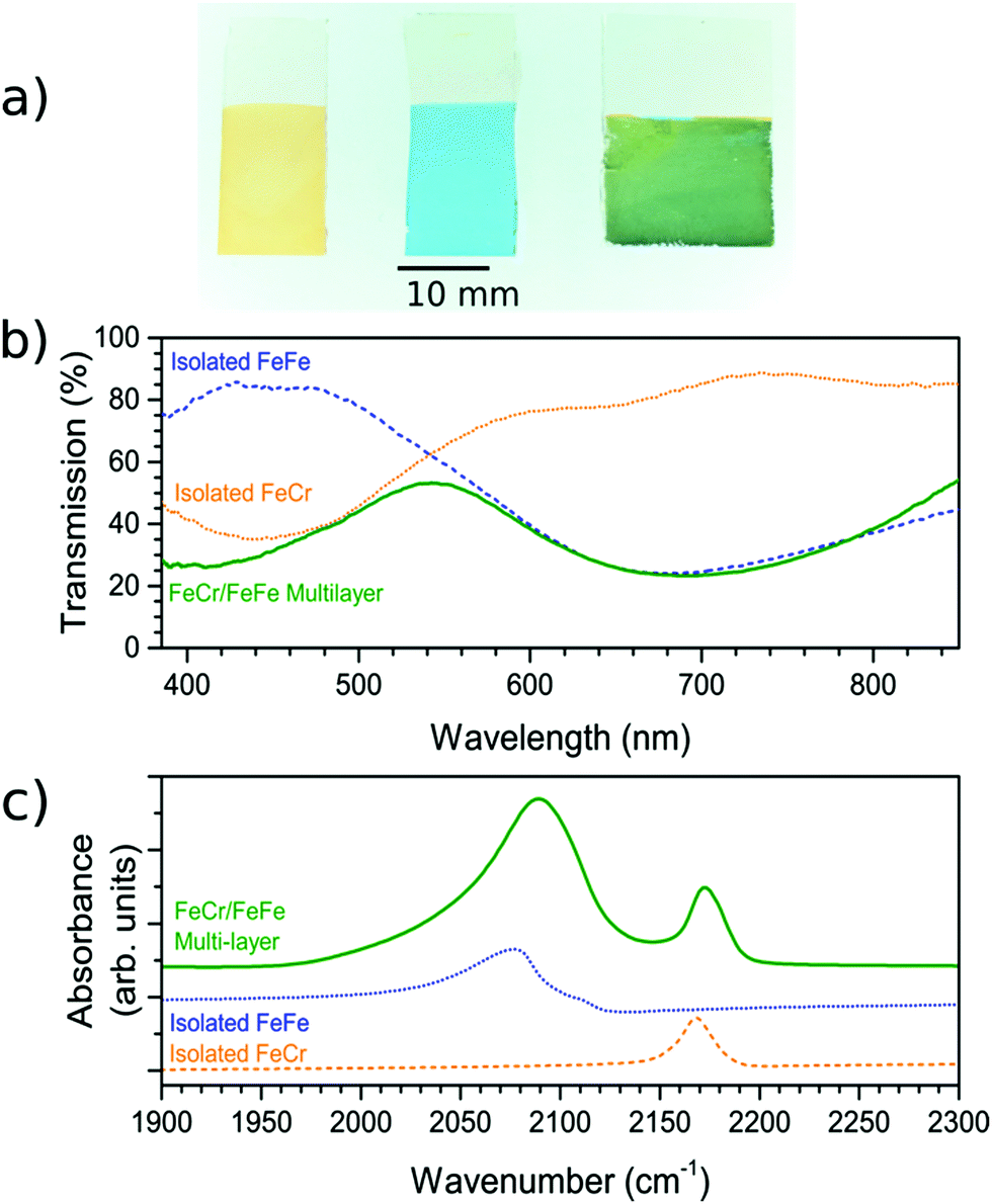 | ||
| Fig. 1 Visible transmission and IR spectra of the individual and the bilayer films. (a) Photos of the FeCr (orange, left), FeFe (blue, middle) and FeCr–FeFe bilayer structure (green, right). (b) Transmission spectra for the FeCr, FeFe films and the bilayer material. (c) The IR spectra showing the CN− stretching frequencies of the FeCr and FeFe films, and those present in the bilayer. The IR spectra have been vertically offset for clarity. | ||
These observations therefore lead us to conclude that we have successfully deposited the FeCr PBA on the FTO electrode. The SEM images of the films indicated that they were polycrystalline with cubic crystals of width ca. 1 μm (Fig. 2a and d). The thickness was determined from AFM and was found to be 300 ± 70 nm. The width of the crystals is larger than the height due to lateral growth of the crystals before growing vertically. Analysis of the SEM images allowed us to estimate that the FeCr layer covers ca. 70–80% of the FTO surface (Fig. S3, ESI†).
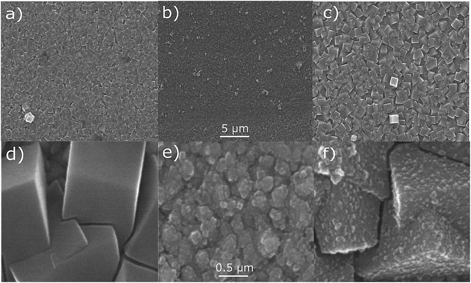 | ||
| Fig. 2 SEM analysis at different zoom levels, showing the FeCr (a and d), FeFe (b and e) and the bilayer films (c and f). The FeFe film can be seen in image (f) as the smaller crystals on the surface of the larger FeCr crystals. The smaller structures visible below the FeCr crystals in (d) is the conductive FTO layer on the glass substrates. 5 μm scale bar refers to images a–c while the 0.5 μm scale bar refers to images d–f. | ||
Deposition of FeFe PB on FeCr PBA
Once the FeCr PBA film was made, cyclic voltammetry in KCl confirmed that there was no electrochemical activity at the voltage needed to make FeFe PB films, which is shown in Fig. 3a. The FeCr PBA is electrochemically active at more negative potentials around −1.0 V vs. SCE, as was shown by Ohkoshi et al.19 After rinsing the FeCr film with deionised water, the deposition of the FeFe film was carried out on top of the FeCr film. The absorption from the FeFe PB could clearly be seen in the transmission spectra as a drop at ca. 685 nm, corresponding to the MMCT transition. The deposition times were tuned to produce films of a similar optical density to the FeCr layer, which resulted in green films (Fig. 1a and b). The optimum deposition time for the FeFe layer was found to be 60 s. The cyclic voltammogram together with a typical absorption spectrum, (Fig. 3a and b), IR spectrum (CN− stretch at 2077 cm−1, Fig. 1c) and the EDX (Fig. S2, ESI†), were all in agreement with the literature and indicated that we had produced FeFe PB on the FeCr PBA surface. The colour of the resulting films ranged from orange (short deposition time), to green (intermediate) and blue (long deposition time).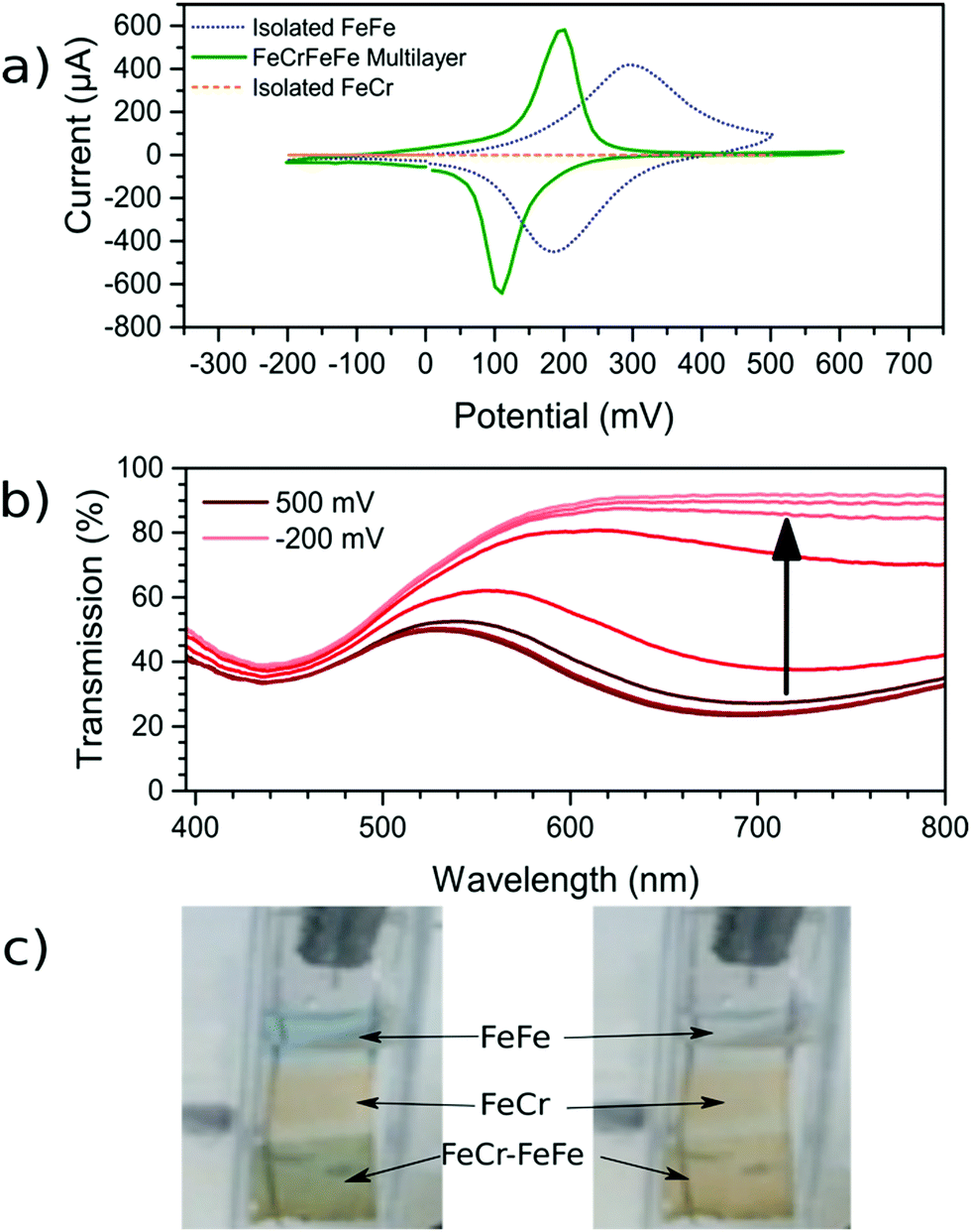 | ||
| Fig. 3 Electrochemical analysis of the films. (a) CV scans (vs. SCE) of both the isolated FeFe film and the FeFe layer as part of the bilayer film. FeCr film shows negligible electrochemical activity over this range. The scan rate used for the three voltammograms was 0.01 V s−1. (b) Spectroelectrochemistry of the bilayer film as the FeFe absorption (685 nm) is electrochemically reduced while the FeCr peak (440 nm) remains unchanged. (c) For demonstration purposes, a sample with FeFe, FeCr and the FeFe–FeCr bilayer was made on the same substrate. The sample was made by masking part of the substrate during the deposition using Teflon tape. When the FeFe layer is electrochemically reduced, the colour is switched from blue to transparent (ESI† video). | ||
Characterisation of bilayer
In order to confirm that a bilayer was formed, the CV was recorded and found to be slightly different compared to a bare FeFe PB film (Fig. 3a). These voltammograms were carried out using Pt pseudo-reference and counter electrodes as this replicates the conditions used in the spectroelectrochemical measurement. The electrochemical behaviour of the FeFe PB is maintained when it is deposited on top of the FeCr PBA film, although we see a shift when it is incorporated into the multilayer structure. The shift in potentials for the peaks could be due to the FeCr electrode having a different electrochemical behaviour to the FTO electrode. There is also a difference in the widths of the peak, the broader peaks of the isolated FeFe film suggest that the process is limited by the diffusion of ions in the solution whereas the switching in the multilayer is limited by the charge passing through the FeCr layer. The CVs do however demonstrate that we have deposited the FeFe PB layer on top of the FeCr film, which confirms that we have formed a true bilayer. This is also seen in the SEM images, where Fig. 2f clearly shows a bilayer with small FeFe crystal grains deposited on the larger FeCr crystal grains. The film-to-substrate ratio of the FeCr film should be even larger than that estimated from the SEM images and is probably larger than at least 80% due to the three-dimensional morphology of the FeCr crystal grains (Fig. S3, ESI†). The surface area of the electrode, which is subsequently used for FeFe PB deposition, is therefore mainly comprised of FeCr sites. This in turn implies that a bilayer is formed. The FeCr PBA is conductive enough, confirmed using tunnelling AFM, to allow the growth of the FeFe PB directly on top of the FeCr crystals (Fig. S4, ESI†). The IR spectrum shows the two peaks at 2077 cm−1 and 2168 cm−1, from the FeFe and FeCr respectively. The EDX also showed the correct composition for both the individual films and the bi-layered films. The FeFe layer thickness was 30 ± 15 nm, determined from AFM of individual films produced under identical conditions to the bilayer film and on an FTO electrode.Optical properties of bilayer
The bilayer films were generally transparent and optically very clear, which therefore make them suitable for optical applications. Interestingly, the SEM and AFM images showed an unexpected difference in the film thicknesses of the two layers despite that the optical density was similar for the two layers. We therefore studied the dependence of the optical density as a function of film thickness, which is shown in Fig. 4. It can be seen that the MMCT oscillator strength for the FeFe material is clearly higher than for the FeCr, which is due to the relative energies and overlap of the orbitals involved in the MMCT absorption.24–26 Based on these data, it appears that the FeCr should be ca. 200 nm thicker than the FeFe films. This is in relatively good agreement with the AFM data, although the SEM images suggests a quite large difference in the size of the crystal grains in the film (Fig. 2f).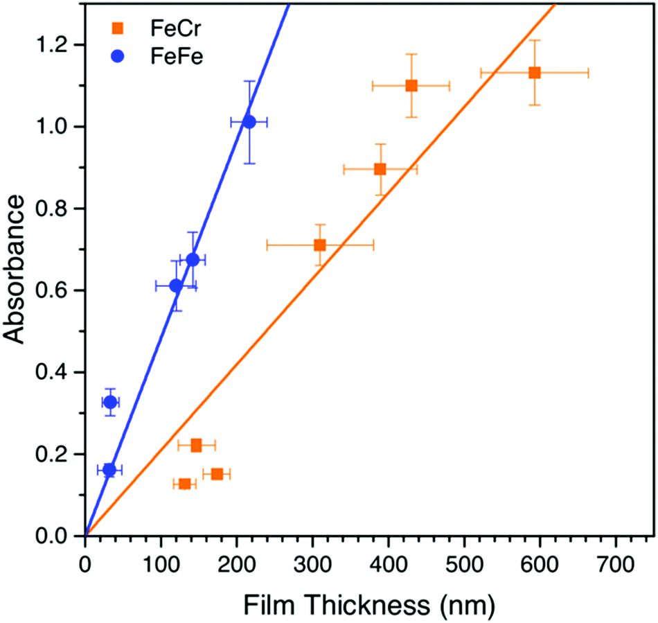 | ||
| Fig. 4 The dependence of the optical density on the thickness of the film for the FeFe and FeCr Prussian blues. The error bars come from the AFM/UV-Vis analysis performed on the deposited samples, many cross sections/spots of the film were taken to reliably estimate these values. Note the error in absorption data increases with larger film thickness due to larger amount of scattered light as the crystals become larger. | ||
Spectroelectrochemistry and electrochromic switching
During the CV scan, it was visually clear that the FeFe PB colour could be completely switched from blue to transparent (ESI† video). The dependence of the optical transmission spectrum on the applied reductive potential is shown in Fig. 3b. As the potential is swept from positive to negative, the absorbance feature at 685 nm, corresponding to the FeFe MMCT disappears as the film is reduced. As the potential is swept in the reverse direction, from negative to positive, the absorbance is restored. Throughout this reversible process, the FeCr film is not affected and retains its colour as it does not undergo any electrochemical redox processes. This can be observed in the CV scan of the isolated FeCr film in Fig. 3a. This therefore demonstrates the successful application of electrochromic PB layer in a PBA multilayered film. Because the vast majority of the FeFe PB crystals are deposited on top of FeCr crystals and because these can be completely reduced, as evidenced by the large colour-change, we conclude that charge is passed from the FeCr layer to the FeFe layer. This therefore implies that there is charge-transfer occurring between the two layers.For the electrochromic switching, potentials of +0.5 V and −0.2 V were chosen from CVs in Fig. 3a, as this will drive the reduction and oxidation of the films to completion in order to measure the switching. The resulting modulation of the absorbance, measured at 685 nm, is shown in Fig. 5a. As can be seen, the colour could be reversibly switched for several cycles without degradation of the film. During the electrochromic switching, there appears to be a certain amount of charge building up in the material, this can be seen in the charge data for the switching process (Fig. S5, ESI†).
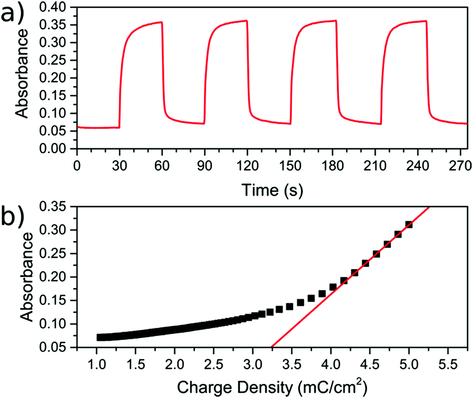 | ||
| Fig. 5 Electrochromic switching and colouration efficiency of the FeCr–FeFe bilayer material. (a) The change in absorbance measured at 685 nm during the electrochromic switching by alternating the potentials between 0.5 to −0.2 V. (b) Colouration efficiency plot of the charge density against the absorbance. The initial gradient of the curve is the colouration efficiency. | ||
The colouration efficiency is a measure of the efficiency of the switching process and is defined as η = ΔOD/ΔQ. This relates the change in the optical density (ΔOD) to the charge (ΔQ) passed through the system. A plot of the absorbance against the supplied charge density will yield η as the initial gradient, as shown in Fig. 5b. The value for η was found to be 147.8 ± 0.8 cm2 C−1, for the blue to bleach process, which is of the same order of magnitude as reported in other studies employing the FeFe PB as part of an electrochromic device.3,27–30 The switching times are defined here as the time taken for 90% of the switch completion. For the blue to bleached state transformation the switching time is 4.4 ± 0.4 s.
Conclusion
We have successfully made bilayers of the FeFe PB and FeCr PBA using electrochemical deposition. When bilayers of equal optical transmission were made, polycrystalline films with thicknesses of 300 nm and 30 nm for the FeCr and FeFe films, respectively, were produced. The crystal grain widths were ca. 1 μm and 30 nm for the FeCr and FeFe layers, respectively. The colour of the FeFe layer could be switched electrically and we found a colouration efficiency of 147.8 ± 0.8 cm2 C−1 and switching time of 4.4 ± 0.4 s for the blue to bleach switch.The demonstration of layer-sensitivity in bilayers of PBAs opens up possibilities to study electron charge-transfer processes in a range of different multilayers of PBAs, some of which are electrochemically active, display high-temperature magnetic ordering, and have bright and chemically tuneable colours. Several PBAs, in addition to those presented here, can be deposited on ITO/FTO coated substrates such as the CrCr,31 VCr17 and CoFe32 PBAs. Layer-sensitive measurements applied to PBAs with novel photomagnetic and optical properties will be of importance for developing applications for photonic and spintronic devices.
Conflicts of interest
There are no conflicts to declare.Acknowledgements
The authors gratefully acknowledge funding from the Royal Society of Edinburgh, the Carnegie Trust (Collaborative Research Grant), EPSRC (studentship to L. H.), and the Royal Society (International Exchange Grant). J. O. J. is a RSE/BP Trust Research fellow.References
- R. J. Mortimer, Annu. Rev. Mater. Res., 2011, 41, 241–268 CrossRef CAS.
- P. R. Somani and S. Radhakrishnan, Mater. Chem. Phys., 2003, 77, 117–133 CrossRef CAS.
- Z. Jiao, J. L. Song, X. W. Sun, X. W. Liu, J. M. Wang, L. Ke and H. V. Demir, Sol. Energy Mater. Sol. Cells, 2012, 98, 154–160 CrossRef CAS.
- A. Pajor-Swierzy, M. Kolasinska-Sojka and P. Warszynski, Colloid Polym. Sci., 2014, 292, 455–465 CAS.
- M. S. Fan, S. Y. Kao, T. H. Chang, R. Vittal and K. C. Ho, Sol. Energy Mater. Sol. Cells, 2016, 145, 35–41 CrossRef CAS.
- M. F. Dumont, E. S. Knowles, A. Guiet, D. M. Pajerowski, A. Gomez, S. W. Kycia, M. W. Meisel and D. R. Talham, Inorg. Chem., 2011, 50, 4295–4300 CrossRef CAS PubMed.
- D. M. Pajerowski, M. J. Andrus, J. E. Gardner, E. S. Knowles, M. W. Meisel and D. R. Talham, J. Am. Chem. Soc., 2010, 132, 4058–4059 CrossRef CAS PubMed.
- J. T. Culp, J. H. Park, I. O. Benitez, M. W. Meisel and D. R. Talham, Polyhedron, 2003, 22, 2125–2131 CrossRef CAS.
- J. P. Prieto-Ruiz, F. M. Romero, H. Prima-Garcia and E. Coronado, J. Mater. Chem. C, 2015, 3, 11122–11128 RSC.
- M. Fitta, H. Prima-Garcia, P. Czaja, T. Korzeniak, M. Krupinski, M. Wojtyniak and M. Balanda, RSC Adv., 2017, 7, 1382–1386 RSC.
- R. C. Millward, C. E. Madden, I. Sutherland, R. J. Mortimer, S. Fletcher and F. Marken, Chem. Commun., 2001, 1994–1995 RSC.
- T. C. Liao, W. H. Chen, H. Y. Liao and L. C. Chen, Sol. Energy Mater. Sol. Cells, 2016, 145, 26–34 CrossRef CAS.
- W. Q. Jin, A. Toutianoush, M. Pyrasch, J. Schnepf, H. Gottschalk, W. Rammensee and B. Tieke, J. Phys. Chem. B, 2003, 107, 12062–12070 CrossRef CAS.
- M. Pyrasch, A. Toutianoush, W. Q. Jin, J. Schnepf and B. Tieke, Chem. Mater., 2003, 15, 245–254 CrossRef CAS.
- W. Zhao, J. J. Xu, C. G. Shi and H. Y. Chen, Langmuir, 2005, 21, 9630–9634 CrossRef CAS PubMed.
- D. M. DeLongchamp and P. T. Hammond, Chem. Mater., 2004, 16, 4799–4805 CrossRef CAS.
- M. Mizuno, S. Ohkoshi and K. Hashimoto, Adv. Mater., 2000, 12, 1955–1958 CrossRef CAS.
- S.-I. Ohkoshi, A. Fujishima and K. Hashimoto, J. Am. Chem. Soc., 1998, 120, 5349–5350 CrossRef CAS.
- S.-I. Ohkoshi, Y. Einaga, A. Fujishima and K. Hashimoto, J. Electroanal. Chem., 1999, 473, 245–249 CrossRef CAS.
- V. D. Neff, J. Electrochem. Soc., 1978, 125, 886–887 CrossRef CAS.
- J. J. Garcia-Jareno, D. Benito, J. Navarro-Laboulais and F. Vicente, J. Chem. Educ., 1998, 75, 881–884 CrossRef CAS.
- L. Hedley, N. Robertson and J. O. Johansson, Electrochim. Acta, 2017, 236, 97–103 CrossRef CAS.
- W. Kosaka, K. Nomura, K. Hashimoto and S.-I. Ohkoshi, J. Am. Chem. Soc., 2005, 127, 8590–8591 CrossRef CAS PubMed.
- M. B. Robin and P. Day, Adv. Inorg. Chem. Radiochem., 1968, 10, 247–422 CrossRef.
- B. Mayoh and P. Day, J. Chem. Soc., Dalton Trans., 1974, 846–852 RSC.
- M. B. Robin, Inorg. Chem., 1962, 1, 337–342 CrossRef CAS.
- T.-S. Tung and K.-C. Ho, Sol. Energy Mater. Sol. Cells, 2006, 90, 521–537 CrossRef CAS.
- M. Deepa, A. Awadhia, S. Bhandari and S. L. Agrawal, Electrochim. Acta, 2008, 53, 7266–7275 CrossRef CAS.
- R. J. Mortimer and T. S. Varley, Sol. Energy Mater. Sol. Cells, 2012, 99, 213–220 CrossRef CAS.
- Y. Rong, S. Kim, F. Su, D. Myers and M. Taya, Electrochim. Acta, 2011, 56, 6230–6236 CrossRef CAS.
- O. Sato, T. Iyoda, A. Fujishima and K. Hashimoto, Science, 1996, 271, 49–51 CAS.
- O. Sato, Y. Einaga, T. Iyoda, A. Fujishima and K. Hashimoto, J. Electrochem. Soc., 1997, 144, L11 CrossRef CAS.
Footnote |
| † Electronic supplementary information (ESI) available. See DOI: 10.1039/c7tc04521b |
| This journal is © The Royal Society of Chemistry 2018 |