Control of oxygen vacancies in ZnO nanorods by annealing and their influence on ZnO/PEDOT:PSS diode behaviour†
Received
19th September 2017
, Accepted 11th November 2017
First published on 2nd February 2018
Abstract
ZnO is one of the most widely studied semiconductors due to its direct wide band gap and high exciton binding energy. Due to its ease of synthesis, robustness and low cost, ZnO has been applied in a wide range of devices, including nanogenerators, solar cells, and photodetectors. In this work, ZnO nanorods were synthesized in a single step using an aqueous method at temperatures below 100 °C. The nanorods were annealed in oxygen and nitrogen and a p-type polymer poly(3,4-ethylenedioxythiophene)polystyrene sulfonate (PEDOT:PSS) was spray coated onto the top of ZnO nanorods to form a p–n junction. The I–V characteristics of the device showed that the annealing atmosphere had a significant effect on the rectification ratio of the device. Further analysis using Mott–Schottky, photoluminescence, and X-ray photoelectron spectroscopy (XPS) indicated that oxygen vacancy concentration correlated well with the free electron density in ZnO as well as the rectification ratio of the p–n junction devices. Devices made with ZnO nanorods annealed in nitrogen had a better rectification ratio than oxygen, representing a simple method to improve p–n junction diode behaviour through tuning the defect properties of the nanorods via controlled annealing.
Introduction
Zinc oxide (ZnO) is a metal-oxide semiconductor with a direct wide band gap and high exciton binding energy. Due to its n-type semiconducting behaviour, radiation hardness, photoconductivity, piezoelectric properties and chemical stability, ZnO is considered as a promising material to be assembled in functional structures such as p–n junctions.1–8 It has been applied in piezoelectric energy harvesting systems,9,10 photodetectors,4 light-emitting diodes11 and photovoltaics.12–14 Nanostructured ZnO has great advantages originating from its large surface-to-volume ratio, high specific surface area and large number of active sites. Many examples of nanostructures have been studied and fabricated as devices: nanoparticles,15 nanorods,16–19 nanowires,13,20,21 nanoplates,22 as well as urchin-like structures23 being the most common.
Many methods have been used to synthesize nanostructured ZnO. They can be mainly classified as vapour-phase deposition and solution-phase synthesis. Vapour-phase deposition such as chemical vapour deposition (CVD),24,25 sputtering26 and pulsed laser deposition27,28 generally require stringent conditions such as high applied voltages, high temperature for the gas phase, and a complex gas-flow system with accurate concentrations. However, more recent developments of vapour-phase deposition methods such as plasma-enhanced CVD have enabled the fabrication of ZnO thin films or nanorods at low temperatures and at large scales.29,30 Solution-phase synthesis is carried out in an aqueous solution containing chemical precursors. Chemical reactions happen in the solution at low temperature resulting in deposition on the substrate. Solution-phase synthesis has many advantages over vapour-phase deposition such as moderate conditions, low cost, easy handling and the potential for scalability. However, many studies have demonstrated that the size and shape are affected by temperature, pH, precursor concentration and duration.16,31,32
ZnO obtained by solution-phase synthesis at low temperature and pressures has many unintentional defects due to their low formation energy.33 Thermal annealing is one of the most popular methods to remove impurities and structural defects from the crystal lattice.34 However, depending on the annealing atmosphere, the defect level in the crystal varies after annealing. Oxygen vacancies with their low formation energy have been invoked as one of the potential factors contributing to the unintentional n-type conductivity of ZnO.35,36
The importance of understanding the defects in ZnO originates from the desire to assemble devices with advantageous electrical, optical and magnetic properties. A p–n junction is a semiconductor structure which allows current to flow only in one direction and is utilized as a fundamental element of most semiconductor devices including diodes, transistors, solar cells and integrated circuits. ZnO can become part of a p–n junction by incorporating it with both organic and inorganic p-type semiconductors. The rectification ratio is represented as the ratio of the forward and reverse current at a specific voltage. The rectification ratio of ZnO nanorod-based diodes with inorganic p-type semiconductors, for example CuSCN, have values of 102–104, while it is less than 10 with organic p-type semiconductors.5,10,34,37–39 The lower rectification ratio of ZnO diodes using organic p-type materials, such as PEDOT:PSS, has been ascribed to the large leakage current caused by recombination sites or trap states at the interface.34 Methods to improve the rectification of these diodes would widen their potential applications, taking advantage of the beneficial properties of the organic p-type semiconductors such as low cost, ease of synthesis/coating, flexibility etc. as well as improving the properties of devices that already use such structures.3,9,40–42
In this work, high aspect ratio ZnO nanorods were synthesized in a single step using an aqueous solution method by altering the synthesis time and precursor concentration. A p–n junction was assembled by spray-coating a poly(3,4-ethylenedioxythiophene) polystyrene sulfonate (PEDOT:PSS) film on the top of the ZnO nanorods. The rectifying behaviour of devices made with ZnO nanorods annealed in nitrogen and oxygen were investigated. The annealing atmosphere was found to affect oxygen vacancies and hence carrier concentration and rectifying behaviour of the p–n junction. This one-step synthesis of ZnO nanorods and control of the diode rectification via the ZnO annealing conditions therefore represents a simple method to produce nanorods with high aspect ratio and improve the performance of a p–n junction.
Experimental
Growth of ZnO nanorods
All the chemicals were purchased from Sigma-Aldrich and used without any further purification. ZnO nanorods were synthesized on FTO-coated glass (Solaronix SA Switzerland, 15 Ω square−1). The substrate was cleaned with acetone and then 2-propanol by ultra-sonication for 15 minutes. A seed layer of zinc acetate was coated on the substrate from a 0.005 M solution in ethanol. The solution was dropped on the substrate and dried with nitrogen, followed by annealing in air at 350 °C for 25 minutes. A thin crystallized ZnO seed layer was formed after annealing. The seeding process was repeated three times. The substrate was suspended face-down in a jar with a solution consisting of equal concentrations of zinc nitrate and hexamethylenetetramine (HMT). Then the jar was placed in a pre-heated oven at 90 °C for a defined time. Afterward, the ZnO nanorods were annealed at 350 °C for 1 hour under different atmospheres (nitrogen and oxygen). The gas flow rate was set to 1 L min−1.
Device fabrication
The substrate was placed on a 100 °C hotplate, and 1 mL of PEDOT:PSS solution (1.3 wt% in water, conductive grade) was deposited on top of the ZnO nanorods using an aerosol spray coating technique. Devices made with a ZnO/PEDOT:PSS p–n junction were completed by evaporating a 100 nm gold contact with an active area of 0.15 cm2 (0.3 cm × 0.5 cm) on the PEDOT:PSS surface using a vacuum thermal evaporator (E306A, Edwards). Regions around the active area were blocked to prevent short circuits using poly(methyl methacrylate) (PMMA, average MW 120![[thin space (1/6-em)]](https://www.rsc.org/images/entities/char_2009.gif) 000), which was dissolved to form a 11 wt% solution in methoxybenzene (99%).
000), which was dissolved to form a 11 wt% solution in methoxybenzene (99%).
Characterization and measurements
The surface and cross-section morphology of ZnO nanorods were examined using a scanning electron microscope (SEM, FEI Inspect F). The average and standard deviation of nanorod diameter and length were calculated by measuring 20 nanorods using ImageJ. The SAED pattern was collected using a transmission electron microscopy (TEM, JEOL JEM 2010). Absorption spectra of ZnO were measured using a UV-Vis Spectrometer (Perkin Elmer, Lamda 950). X-ray diffraction (XRD) patterns of ZnO on FTO coated glass were obtained with a Panalytical Xpert Pro diffractometer using Cu Kα radiation. High resolution X-ray photoelectron spectroscopy (XPS) was carried out using a Thermo Scientific K-Alpha+. XPS data were analysed by CasaXPS™ software with a calibrated C 1s peak of 284.6 eV. Mott–Schottky measurements were performed by a potentiostat (Gamry Potentiostat Interface 1000) with a three-electrode setup; a Ag/AgCl electrode and a glassy carbon rod electrode were used as reference and counter electrode, respectively. 0.01 M Na2SO4 (pH 6.8) was used as the electrolyte. Photoluminescence (PL) was excited using ∼6 ns pulses at 10 Hz from a frequency-tripled Nd:YAG laser (355 nm). Luminescence was dispersed in a Triax 550 monochromator and detected using a Hamamatsu R5509-73 photomultiplier. The resulting signal was captured on a LeCroy Waverunner-2 Oscilloscope and the whole decay curve integrated to give the PL intensity. Individual decay curves were fitted to investigate decay dynamics. Voltage-current characteristics of the p–n junction were measured using a source meter (Keithley 2400) controlled by a custom-written LabVIEW program in the range of −1.5 to +1.5 V at room temperature.
Results and discussion
The chemical reactions of ZnO nanorods by aqueous solution method at low temperature (<100 °C) are summarized in the following equations:43,44| | | (CH2)6N4 + H2O → 6HCHO + 4NH3 | (1) |
| | | NH3 + H2O ↔ NH4+ + OH− | (2) |
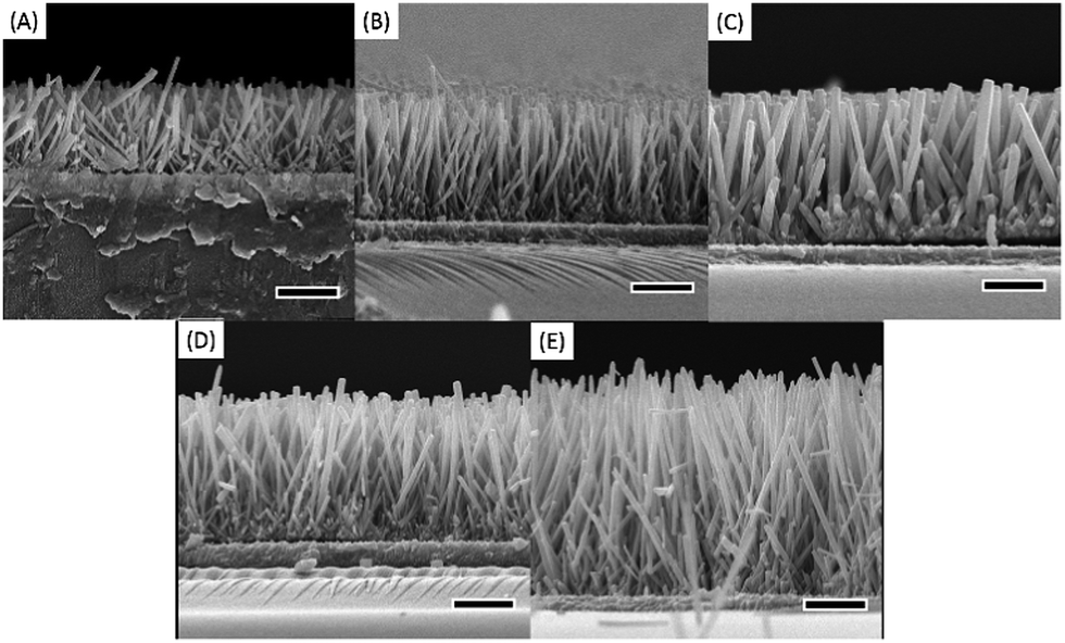
Eqn (1) and (2) are the decomposition reactions of HMT that acts as a pH buffer to supply ammonia and hydroxyl ions. ZnO nanorods grow viaeqn (3) and (4) on the base of the crystallized ZnO seed layer. The effect of the seed layer and solution pH on ZnO growth have been investigated previously.16 It was reported that crystallized ZnO acting as seed layer on the substrate played a vital role due to the preferred (001) crystal face with low growth energy. To achieve ZnO nanorods with high aspect ratio, one of the most commonly-used methods is to refresh the growth solution to extend the length of the rods, with the assumption that the reaction ceases after around 2.5 h when homogeneous precipitation ceases.10,13 However, here we have studied a range of synthesis times and precursor concentrations to find the optimum conditions to achieve high-aspect-ratio ZnO nanorods using only a single growth step. Fig. 1 shows cross-section morphologies of the ZnO nanorods arrays when the synthesis time and precursor concentration were altered. A uniform and dense array of ZnO nanorods was formed on seeded FTO-coated glass. The average diameter, length and aspect ratio are summarized in Table 1. The nanorods synthesized at 50 mM showed lower aspect ratio compared to 10 mM and 25 mM. This can be explained by the growth of the non-polar face being less inhibited at high Zn2+ concentration, thus the ZnO nanorod diameter increased faster than at lower concentrations. The highest aspect ratio was achieved at a concentration of 25 mM, therefore further investigating longer reaction times shows that the length increased with duration while the diameter showed no significant change, thus increasing the aspect ratio. The highest aspect ratio of 51 was achieved when using a 25 mM, pH 6 solution for 24 hours.
 |
| | Fig. 1 Cross-section SEM morphologies of ZnO nanorods synthesis. (A) 8 h, 10 mM, (B) 8 h, 25 mM, (C) 8 h, 50 mM, (D) 16 h, 25 mM, (E) 24 h, 25 mM. The scale bar is 1 μm. | |
Table 1 Diameter, length, and aspect ratio of ZnO nanorods synthesized by different concentration and duration
| Duration (h) |
Precursor concentration (mM) |
Diameter (nm) |
Length (μm) |
Aspect ratio |
| 8 |
10 |
71.7 ± 2.7 |
1.6 ± 0.02 |
22 |
| 25 |
74.0 ± 1.5 |
2.0 ± 0.01 |
27 |
| 50 |
123.7 ± 2.6 |
2.5 ± 0.03 |
20 |
|
|
| 16 |
25 |
75.3 ± 2.0 |
2.5 ± 0.01 |
33 |
| 24 |
25 |
78.4 ± 2.7 |
4.0 ± 0.03 |
51 |
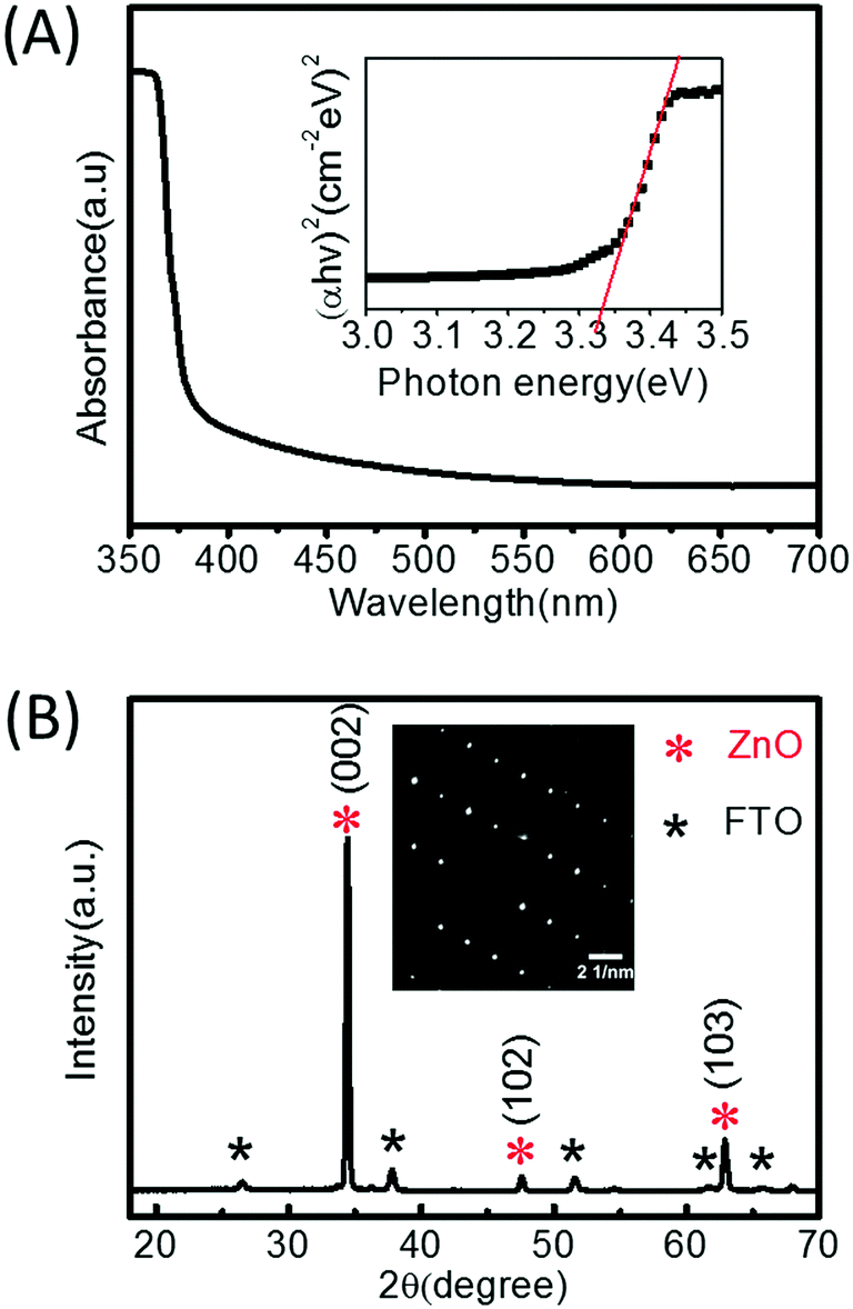
The nanorods with the highest aspect ratio (24 h, 25 mM) were further analysed by UV-Vis absorption, X-ray diffraction and transmission electron microscopy (Fig. 2). Fig. 2(A) shows a typical ZnO absorption spectrum between 350–700 nm, and a direct band gap (Eg) of 3.34 eV was determined from the inset Tauc-plot. The value of Eg agrees well with previous work where the growth solution was refreshed to extend the nanorods.4 A wurtzite crystal structure with preferred orientation in the c-axis was confirmed by the dominant (002) peak at 34.4° in the XRD pattern (JCPDS 36-1451) (Fig. 2(B)). The inset SAED pattern in Fig. 2(B) also demonstrates that the nanorods array was highly crystalized.
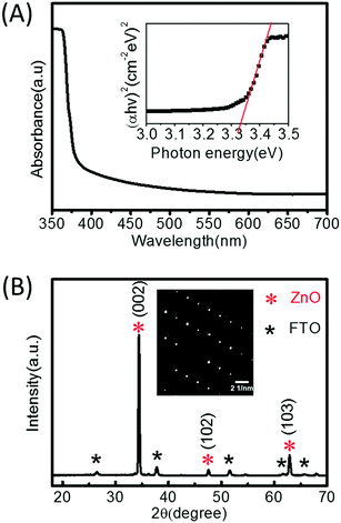 |
| | Fig. 2 (A) UV-Vis absorption spectroscopy, inset Tauc-plot, and (B) XRD patterns, inset SAED diffraction patterns of ZnO nanorods. | |
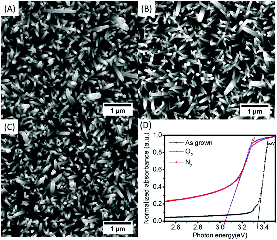
ZnO nanorods synthesized by aqueous methods at low temperature (<100 °C) contain defects both in the bulk structure and surface states.1,33,45 Thermal treatment is one of the most effective methods to remove these defects. In this work, annealing of ZnO nanorods at 350 °C for 1 hour in nitrogen and oxygen was investigated. Fig. 3(A)–(C) display the morphology of ZnO after annealing. There was no significant change on the surface of the ZnO, which differs from ZnO nanorods synthesized in a pH 11 growth solution.34 However, as shown in the Tauc-plots of Fig. 3(D), the band gap of ZnO nanorods annealed in N2 and O2 were the same, both decreasing by 0.29 eV compared to as-grown nanorods.
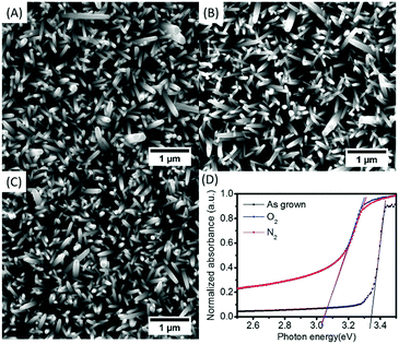 |
| | Fig. 3 Top view SEM morphologies of ZnO nanorods: (A) as-grown, (B) annealed in nitrogen, and (C) annealed in oxygen, (D) Tauc-plots of ZnO annealing in N2, O2, and as grown. | |
In order to compare the effect of the annealing conditions of these nanorods to the electrical properties, an organic semiconducting polymer, PEDOT:PSS, was spray coated on the surface of the ZnO nanorods. Fig. 4(A) depicts the cross-section of the ZnO/PEDOT:PSS structure, where the thickness of the p-type polymer layer was approximately 1 μm, and the gold contact 100 nm. As can been seen, the PEDOT:PSS layer penetrated partially into the nanorods to make good contact with tips of the n-type ZnO nanorods. It is known that polystyrene sulfonate (PSS) is an acid due to the sulfonic acid group and may therefore etch the ZnO nanorods. From Fig. 4(A), the tips of ZnO nanorods are still well-defined; furthermore SEM analysis of nanorods separated from the PEDOT:PSS (Fig. S1, ESI†) shows that there were rod-shaped holes in the PEDOT:PSS layer and also the nanorod tips still embedded within the PEDOT:PSS film, which proved that the PEDOT:PSS did not etch the tips of the ZnO nanorods. The I–V characteristics of p–n junctions made of ZnO and PEDOT:PSS were measured at bias voltages between −1.5 and 1.5 V (Fig. 4(B)). The rectifying behaviour shown in the I–V curves confirmed that diodes were successfully produced. The device rectification ratios at ±1.5 V of ZnO nanorods annealed in the different atmospheres are shown in Table 2. The rectification ratio of the as-grown sample was 2.1 at ±1.5 V, while it was improved to be 28.8 and 38 by thermal treatment of ZnO in oxygen and nitrogen. While these values are low compared to all-inorganic diodes made with ZnO nanorods discussed above, they are high compared to previous ZnO/PEDOT:PSS diodes.9,10 This therefore demonstrates the benefit of careful control of the ZnO composition through annealing for diode performance.
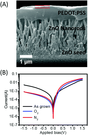 |
| | Fig. 4 (A) Cross-section view of a ZnO/PEDOT:PSS junction (gold layer indicated with red lines), (B) I–V characteristics of device made with ZnO annealed in different atmospheres. | |
Table 2 Device rectification ratio, carrier concentration, and O 1s peak information of ZnO annealed in different atmosphere. Average and standard deviations of recitification ratio were taken from measurements of three devices for each condition
|
|
As-grown |
Oxygen |
Nitrogen |
| Rectification ratio at ±1.5 V |
2.1 ± 0.7 |
28.8 ± 0.4 |
38.0 ± 0.4 |
| Carrier concentration (1019 cm−3) |
0.7 |
1.7 |
3.9 |
| Oxide in lattice (at%) |
52.7 |
54.2 |
52.2 |
| Oxygen vacancy (at%) |
27.2 |
26.6 |
35.8 |
| Adsorbed oxygen (at%) |
20.1 |
19.2 |
12.1 |
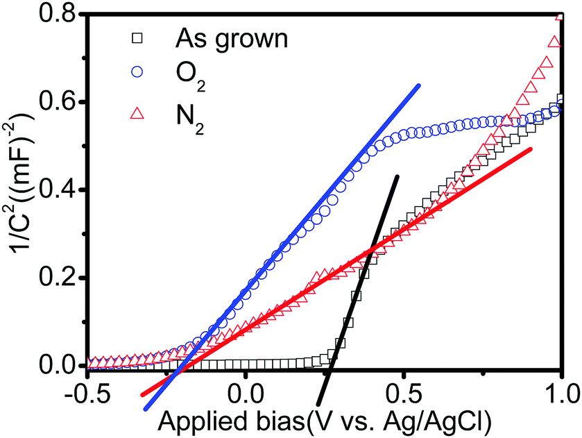
To understand the influence of the annealing atmosphere on the rectifying property of devices made with ZnO nanorods, electrochemical impedance measurements were carried out to determine the capacitance of ZnO when in contact with an electrolyte. The Mott–Schottky equation was used to calculate the carrier concentration from these data:46
| |  | (5) |
where
e0 is the electron charge,
ε the dielectric constant of ZnO,
ε0 the permittivity of vacuum,
Nd the carrier concentration,
V the applied potential,
Vfb the flatband potential, and
kT/
e0 is a temperature-dependent correction term. According to the Mott–Schottky equation,
Nd is determined from the slope in the plot shown in
Fig. 5. The positive slopes confirmed that all ZnO nanorods obtained were n-type regardless of the annealing atmosphere. The carrier concentration was calculated and is summarized in
Table 2. The carrier concentration was highest in ZnO nanorods annealed in nitrogen, followed by oxygen and as-grown. It is of interest that the trend in the carrier concentration of ZnO after annealing correlated well with the device rectification ratio.
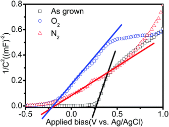 |
| | Fig. 5 Mott–Schottky plots of ZnO annealed in different atmospheres. | |
To investigate this relationship further, the O 1s peaks in three different samples were studied by high-resolution XPS (Fig. 6). The O 1s peaks showed significant changes after annealing in nitrogen and oxygen; a shoulder appeared in the O 1s peak towards the higher energy direction. The O 1s peak was fitted using Gaussian fitting to three peaks, which were centred at 530.0 eV, 531.1 eV, and 532.1 eV. The peak at 530.0 eV corresponds to lattice oxygen anions (O2−) in the wurtzite structure, the peak at 531.1 eV has been attributed to Ox− (O2− and O−) ions in the oxygen-deficient regions caused by oxygen vacancies, and the peak at 532.1 eV corresponds to adsorbed oxygen at the surface.25 The amount of oxygen species in different samples are listed in Table 2. The oxygen vacancy content clearly decreased in ZnO with increased oxygen partial pressure in the annealing atmosphere, while the amount of adsorbed oxygen decreased during nitrogen annealing, as expected in a low oxygen partial pressure environment. The decrease in oxygen vacancies during annealing under high oxygen partial pressure can be explained by reactions between oxygen in the annealing gas and uncoordinated zinc at these sites on the surface, followed by diffusion of oxygen ions into the crystal structure to oxygen deficient regions. The converse effect occurs during nitrogen annealing, where the low oxygen partial pressure leads to loss of oxygen at the surface, and a subsequent increase in oxygen vacancies. The amount of carbon on the ZnO surface was also influenced by the annealing atmosphere, which was 49.8% in as grown ZnO, 40.0% in ZnO annealed in O2, and 51.0% in ZnO annealed in N2. When annealing in O2 carbon-containing compounds on the surface will react with oxygen to be converted to COx and escape from the surface, resulting in a decrease of the amount of carbon.
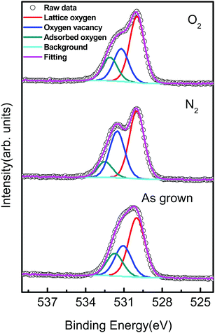 |
| | Fig. 6 High-resolution O 1s XPS spectra of ZnO nanorods annealed in different atmospheres. This provides strong evidence that the main source of n-type doping in these nanorods is oxygen vacancies, as previously identified for ZnO.35,36 | |
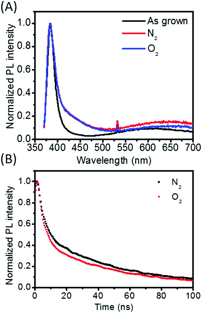
To understand the photophysics of the ZnO nanorods, steady-state and time-resolved photoluminescence spectroscopy was carried out on ZnO/PEDOT:PSS diodes using a 355 nm excitation wavelength. The normalized PL in Fig. 7(A), shows a strong near band-edge emission at ∼380 nm for all samples. The intensity of deep level emission in ZnO nanorods between 500–700 nm was observed to increase after annealing, slightly more so for nitrogen compared to oxygen annealing. Comparing this to the XPS results, this implies that in these samples the PL emission centred at 650 nm corresponds to oxygen-vacancy-related emission as their concentration is highest in the nitrogen-doped sample. PL lifetime for all main emissions seen in the as-grown nanorods were too short to measure using the 5 ns laser pulse, implying a lifetime of <5 ns. A measureable PL lifetime of annealed samples was found at 430 nm, giving 53.0 ns for nitrogen, and 51.9 ns for oxygen (Fig. 7(B)). Therefore the use of annealing in either nitrogen or oxygen has clearly reduced recombination rate, which is beneficial for many device applications. However, there is a negligible difference in the lifetime of samples annealed in nitrogen or oxygen at the timescale measured. This implies that oxygen-defect-induced carrier density is the main factor leading to the improved rectification of the diodes when annealed in nitrogen, as discussed above, not reduced recombination. However, ultra-fast spectroscopy could be studied in future to identify whether there is a difference in recombination at faster timescales, particularly where optoelectronic application may be of interest.
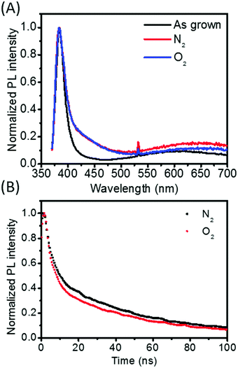 |
| | Fig. 7 (A) Integrated photoluminescence spectra of ZnO/PEDOT:PSS annealed in different atmospheres and (B) photoluminescence decay measured at an emission wavelength of 430 nm. | |
Comparing the Mott–Schottky, XPS, and PL results, there is a clear correlation between increased oxygen vacancies with low oxygen partial pressure annealing and high carrier concentration. Consequently, the different annealing atmospheres clearly have an effect on the carrier concentration of ZnO nanorods as well as the performance of the diode structures. Hence the improved diode performance can be directly related to the increase in the oxygen-vacancy-related doping level in the ZnO crystal structure with decreased oxygen partial pressure during annealing.
Conclusions
ZnO nanorods were synthesized using aqueous solution methods using a single step for 24 hours. Compared with the conventional method, which refreshes the growth solution to extend the nanorods, the as-achieved nanorods using a single step showed no significant difference in SEM morphology, UV-Vis absorption spectroscopy, XRD patterns, and SAED diffractions. The annealing atmosphere was related to the n-type carrier concentration and oxygen vacancy content using Mott–Schottky, PL, and XPS analysis. The carrier concentration of the ZnO nanorods and the rectification ratio in ZnO/PEDOT:PSS diodes increased with the decreasing oxygen partial pressure during annealing. These results clearly demonstrate that high aspect ratio ZnO nanorods can be produced in a single reaction step, and that by increasing the intrinsic oxygen vacancy-related defects through nitrogen annealing, high carrier concentration rods can be produced leading to improved diode performance. This indicates a promising route for a wide range of applications that can make use of such improved ZnO nanorod-based diode performance. While we have focussed on the optimisation of the ZnO nanorods to improve the rectification ratio of ZnO/PEDOT:PSS diodes in this work, further improvements of these devices would be achieved by control of the PEDOT:PSS properties, such as doping levels, which would be an interesting avenue for future work.
Conflicts of interest
There are no conflicts to declare.
Acknowledgements
Y. Tu would like to thank the China Scholarship Council/Queen Mary University of London Joint PhD scholarship program. S. Q. Chen thanks the China Postdoctoral Science Foundation (2017M610729) for financial support. J. Briscoe acknowledges funding from Innovate UK (38164-262219). The authors thank Thermo Scientific for carrying out the XPS measurements.
Notes and references
- J. Wang, X. Li, Y. Xia, S. Komarneni, H. Chen, J. Xu, L. Xiang and D. Xie, ACS Appl. Mater. Interfaces, 2016, 8, 8600–8607 CAS
 .
.
- M. W. Hoffmann, L. Mayrhofer, O. Casals, L. Caccamo, F. Hernandez-Ramirez, G. Lilienkamp, W. Daum, M. Moseler, A. Waag, H. Shen and J. D. Prades, Adv. Mater., 2014, 26, 8017–8022 CrossRef CAS PubMed .
- N. Jalali, P. Woolliams, M. Stewart, P. M. Weaver, M. G. Cain, S. Dunn and J. Briscoe, J. Mater. Chem. A, 2014, 2, 10945 CAS .
- S. M. Hatch, J. Briscoe and S. Dunn, Adv. Mater., 2013, 25, 867–871 CrossRef CAS PubMed .
- S. M. Hatch, J. Briscoe and S. Dunn, Thin Solid Films, 2013, 531, 404–407 CrossRef CAS .
- P. Lin, X. Yan, Z. Zhang, Y. Shen, Y. Zhao, Z. Bai and Y. Zhang, ACS Appl. Mater. Interfaces, 2013, 5, 3671–3676 CAS .
- S. N. Das, J.-H. Choi, J. P. Kar, K.-J. Moon, T. I. Lee and J.-M. Myoung, Appl. Phys. Lett., 2010, 96, 092111 CrossRef .
- M. Wang and X. Wang, Sol. Energy Mater. Sol. Cells, 2008, 92, 766–771 CrossRef CAS .
- J. Briscoe, N. Jalali, P. Woolliams, M. Stewart, P. M. Weaver, M. Cain and S. Dunn, Energy Environ. Sci., 2013, 6, 3035 CAS .
- J. Briscoe, M. Stewart, M. Vopson, M. Cain, P. M. Weaver and S. Dunn, Adv. Energy Mater., 2012, 2, 1261–1268 CrossRef CAS .
- J. Joo, B. Y. Chow, M. Prakash, E. S. Boyden and J. M. Jacobson, Nat. Mater., 2011, 10, 596–601 CrossRef CAS PubMed .
- S. Shoaee, J. Briscoe, J. R. Durrant and S. Dunn, Adv. Mater., 2014, 26, 263–268 CrossRef CAS PubMed .
- M. Law, L. E. Greene, J. C. Johnson, R. Saykally and P. Yang, Nat. Mater., 2005, 4, 455–459 CrossRef CAS PubMed .
- D. Bi, G. Boschloo, S. Schwarzmuller, L. Yang, E. M. Johansson and A. Hagfeldt, Nanoscale, 2013, 5, 11686–11691 RSC .
- M. Sturaro, E. Della Gaspera, N. Michieli, C. Cantalini, S. M. Emamjomeh, M. Guglielmi and A. Martucci, ACS Appl. Mater. Interfaces, 2016, 8, 30440–30448 CAS .
- B. Weintraub, Z. Zhou, Y. Li and Y. Deng, Nanoscale, 2010, 2, 1573–1587 RSC .
- B. Yang, P. Feng, A. Kumar, R. S. Katiyar and M. Achermann, J. Phys. D: Appl. Phys., 2009, 42, 195402 CrossRef .
- J. X. Wang, X. W. Sun, Y. Yang, H. Huang, Y. C. Lee, O. K. Tan and L. Vayssieres, Nanotechnology, 2006, 17, 4995–4998 CrossRef CAS .
- Y. Tak and K. Yong, J. Phys. Chem. B, 2005, 109, 19263–19269 CrossRef CAS PubMed .
- R. Zhu, W. Zhang, C. Li and R. Yang, Nano Lett., 2013, 13, 5171–5176 CrossRef CAS PubMed .
- Q. Wan, Q. H. Li, Y. J. Chen, T. H. Wang, X. L. He, J. P. Li and C. L. Lin, Appl. Phys. Lett., 2004, 84, 3654 CrossRef CAS .
- Z. Jing and J. Zhan, Adv. Mater., 2008, 20, 4547–4551 CrossRef CAS .
- D. Barreca, D. Bekermann, E. Comini, A. Devi, R. A. Fischer, A. Gasparotto, C. Maccato, C. Sada, G. Sberveglieri and E. Tondello, CrystEngComm, 2010, 12, 3419 RSC .
- S. Chen, M. McLachlan, A. Sapelkin and R. Binions, J. Mater. Chem. A, 2015, 3, 22311–22315 CAS .
- S. Chen, M. E. A. Warwick and R. Binions, Sol. Energy Mater. Sol. Cells, 2015, 137, 202–209 CrossRef CAS .
- T. Ohshima, T. Maeda, Y. Tanaka, H. Kawasaki, Y. Yagyu, T. Ihara and Y. Suda, Jpn. J. Appl. Phys., 2016, 55, 01AA08 CrossRef .
- J. B. Franklin, B. Zou, P. Petrov, D. W. McComb, M. P. Ryan and M. A. McLachlan, J. Mater. Chem., 2011, 21, 8178 RSC .
- A. Ohtomo and A. Tsukazaki, Semicond. Sci. Technol., 2005, 20, S1–S12 CrossRef CAS .
- M. Macias-Montero, A. Borras, Z. Saghi, P. Romero-Gomez, J. R. Sanchez-Valencia, J. C. Gonzalez, A. Barranco, P. Midgley, J. Cotrino and A. R. Gonzalez-Elipe, J. Mater. Chem., 2012, 22, 1341–1346 RSC .
- P. Romero-Gómez, J. Toudert, J. R. Sánchez-Valencia, A. Borrás, A. Barranco and A. R. Gonzalez-Elipe, J. Phys. Chem. C, 2010, 114, 20932–20940 Search PubMed .
- Y. Zhang, M. K. Ram, E. K. Stefanakos and D. Y. Goswami, J. Nanomater., 2012, 1–22 Search PubMed .
- G. Amin, M. H. Asif, A. Zainelabdin, S. Zaman, O. Nur and M. Willander, J. Nanomater., 2011, 1–9 Search PubMed .
- L. Schmidt-Mende and J. L. MacManus-Driscoll, Mater. Today, 2007, 10, 40–48 CrossRef CAS .
- S. M. Hatch, J. Briscoe, A. Sapelkin, W. P. Gillin, J. B. Gilchrist, M. P. Ryan, S. Heutz and S. Dunn, J. Appl. Phys., 2013, 113, 204501 CrossRef .
- S. E. Harrison, Phys. Rev., 1954, 93, 52–62 CrossRef CAS .
- A. R. Hutson, Phys. Rev., 1957, 108, 222–230 CrossRef CAS .
- Z. Yang, M. Wang, J. Ding, Z. Sun, L. Li, J. Huang, J. Liu and J. Shao, ACS Appl. Mater. Interfaces, 2015, 7, 21235–21244 CAS .
- J. Garnier, R. Parize, E. Appert, O. Chaix-Pluchery, A. Kaminski-Cachopo and V. Consonni, ACS Appl. Mater. Interfaces, 2015, 7, 5820–5829 CAS .
- B. K. Sharma, N. Khare and S. Ahmad, Solid State Commun., 2009, 149, 771–774 CrossRef CAS .
- M. Choi, G. Murillo, S. Hwang, J. W. Kim, J. H. Jung, C. Y. Chen and M. Lee, Nano Energy, 2017, 33, 462–468 CrossRef CAS .
- X. H. Ren, H. Q. Fan, Y. W. Zhao and Z. Y. Liu, ACS Appl. Mater. Interfaces, 2016, 8, 26190–26197 CAS .
- I. J. No, D. Y. Jeong, S. Lee, S. H. Kim, J. W. Cho and P. K. Shin, Microelectron. Eng., 2013, 110, 282–287 CrossRef CAS .
- Q. C. Li, V. Kumar, Y. Li, H. T. Zhang, T. J. Marks and R. P. H. Chang, Chem. Mater., 2005, 17, 1001–1006 CrossRef CAS .
- A. Zainelabdin, S. Zaman, G. Amin, O. Nur and M. Willander, Cryst. Growth Des., 2010, 10, 3250–3256 CAS .
- L. E. Greene, M. Law, J. Goldberger, F. Kim, J. C. Johnson, Y. Zhang, R. J. Saykally and P. Yang, Angew. Chem., 2003, 42, 3031–3034 CrossRef CAS PubMed .
- M. C. K. Sellers and E. G. Seebauer, Thin Solid Films, 2011, 519, 2103–2110 CrossRef CAS .
Footnote |
| † Electronic supplementary information (ESI) available. See DOI: 10.1039/c7tc04284a |
|
| This journal is © The Royal Society of Chemistry 2018 |
Click here to see how this site uses Cookies. View our privacy policy here. 
 Open Access Article
 This Open Access Article is licensed under a
  a,
Shuqun
Chen
b,
Xuan
Li
a,
Jelena
Gorbaciova
c,
William P.
Gillin
c,
Steffi
Krause
a,
Shuqun
Chen
b,
Xuan
Li
a,
Jelena
Gorbaciova
c,
William P.
Gillin
c,
Steffi
Krause