
 Open Access Article
 This Open Access Article is licensed under a
 Creative Commons Attribution 3.0 Unported Licence
Aluminium/gallium, indium/gallium, and aluminium/indium co-doped ZnO thin films deposited via aerosol assisted CVD
Dominic B.
Potter
 ,
Michael J.
Powell
,
Ivan P.
Parkin
and
Claire J.
Carmalt
*
,
Michael J.
Powell
,
Ivan P.
Parkin
and
Claire J.
Carmalt
*
Materials Chemistry Centre, Department of Chemistry, University College London, 20 Gordon Street, London, WC1H 0AJ, UK. E-mail: c.j.carmalt@ucl.ac.uk
First published on 4th January 2018
Abstract
Aluminium/gallium co-doped ZnO (AGZO), indium/gallium co-doped ZnO (IGZO), and aluminium/indium co-doped ZnO (AIZO) thin films were synthesised on glass substrates via aerosol assisted chemical vapour deposition (AACVD). The films were fully characterised by X-ray diffraction, X-ray photoelectron spectroscopy and scanning electron microscopy. The optoelectronic properties of the films were determined using UV/vis spectroscopy and Hall effect measurements. The AGZO film displayed the lowest resistivity (1.3 × 10⁻² Ω cm) and highest carrier mobility (7.9 cm2 V−1 s−1), due the relatively low amount of disorder in the structure. The incorporation of In3+ resulted in the most disorder in the structure due to its large radius, which led to an increase in optical absorption, and a decrease in resistivity.
Introduction
Doped zinc oxide is a widely investigated material, due to its potential as a sustainable transparent conducting oxide (TCO). TCOs are materials which are both optically transparent and electrically conductive – two properties which are usually mutually exclusive.1 This combination of functional properties means that TCOs have a broad range of applications in photovoltaic devices, such as solar cells, touch screens, light-emitting diodes (LEDs) and liquid crystal displays (LCDs).2,3 Commercially, the two most commonly used TCO materials are tin-doped indium oxide (ITO) and fluorine-doped tin oxide (FTO). However, the price of both indium and tin are relatively high and unstable compared to zinc.4 For this reason, there has been extensive research done into ZnO, due to its inherent n-type conductivity,5–7 as well as its wide, direct band gap (ca. 3.37 eV at room temperature),8–10 low cost,11–13 and relatively low toxicity,14–16 all of which make it appealing for industrial processes.Many dopants have been screened to improve the electrical properties of ZnO. The most common of these are the group 13 elements: aluminium, gallium and indium. These dopants are introduced as substitutional defects on zinc sites.17 Aluminium-doped ZnO (AZO), gallium-doped ZnO (GZO), and indium-doped ZnO (IZO) thin films have been prepared by various techniques, including magnetron sputtering,18–20 pulsed laser deposition (PLD),21–23 molecular beam epitaxy (MBE),24,25 atomic layer deposition (ALD),26–28 spray pyrolysis,29,30 atmospheric pressure chemical vapour deposition (APCVD),31–33 and aerosol assisted chemical vapour deposition (AACVD).34–36
Moreover, co-doped ZnO films have been prepared using these dopants. Co-doping allows the benefits of two dopants to be exploited simultaneously. The strengths of one dopant can compensate for the weaknesses of another. For example, aluminium is the third most abundant element in the Earth's crust.37 Hence, it is can be purchased at a lower cost than gallium and indium. Furthermore, aluminium has a relatively low toxicity compared to the other elements of group 13.38 Additionally, AZO films tend to be more conductive than GZO and IZO films.39–41 However, the high reactivity of aluminium may lead to unwanted side reactions during film growth.42
Conversely, gallium is a relatively stable dopant element, which means the potential for unwanted side reactions is lower compared to other dopants.43–45 Nomoto et al. found that, when exposed to 85% humidity at 85 °C for 1000 hours, the resistivity of GZO films were more stable in comparison to AZO films.46 Another benefit of using gallium as the dopant for ZnO is that the radius of 4-coordinate Ga3+ (0.62 Å) is closer to that of 4-coordinate Zn2+ (0.74 Å), in comparison to Al3+ (0.53 Å) and In3+ (0.81 Å).47 For this reason, it typically results in fewer lattice distortion and crystal defects when it substitutes for Zn2+.48
Aluminium/gallium co-doped ZnO (AGZO),49–51 indium/gallium co-doped ZnO (IGZO),52–55 and aluminium/indium co-doped ZnO (AIZO)56–58 thin films have been prepared previously by various techniques. However, until this study, they had not been synthesised via AACVD. AACVD is a technique which has several advantages over traditional APCVD. AACVD relies on dissolving the precursors and then generating an aerosol mist from the solution. Hence, the main benefit of AACVD is that a wide range of non-volatile precursors can be used to deposit a film at a low cost. Additionally, it is relatively easy to control the stoichiometry of dopants, since the amount of dopant incorporated into the film is related to the amount used in solution. In general, a higher dopant concentration in solution leads to a higher dopant concentration in the resultant film. Finally, neither the precursors, nor the lines leading to the reactor need to be heated, and hence AACVD is a relatively low-cost technique, through which films can be deposited with ease.59,60 In addition, recent work by Powell et al. has demonstrated that AACVD can be used to deposit films with high growth rates (ca. 100 nm min−1), making the technique suitable for certain industrial depositions.61
In this paper, AGZO, IGZO, and AIZO thin films were deposited via AACVD for the first time. This was also the first time where all three of these materials were synthesised under the same conditions, which has allowed for an unprecedented and thorough comparison of the three co-doped materials. The effects of aluminium, gallium, and indium were investigated with respect to the crystal and grain growth of the films, and the resultant optoelectronic properties. The effects of the dopants can be related to lattice distortion, based on the different ionic radii.
Experimental
Film synthesis
Aerosol assisted chemical vapour deposition (AACVD) was set up as described previously.36,62 All chemicals were purchased from Sigma-Aldrich, and were used as-bought, without any further purification. A typical precursor solution was made by dissolving Zn(acac)2 (0.50 g, 1.90 mmol) in methanol (20 mL). Following this, dopant quantities of MCl3 (M = Al, Ga, In) were dissolved in the solution. It was observed previously that 10 mol% dopant led to superior optoelectronic properties of AZO, GZO, and IZO thin films deposited via AACVD.36 For this reason, the total dopant concentration for the co-doped films was kept at 10 mol%. Acetic acid (1 mL) was added to prevent hydrolysis of the Zn(acac)2. The solution was stirred for at least 10 minutes in a glass bubbler. The substrate used was a 3.2 mm thick float glass plate (Pilkington Technology Management Limited, Lancashire, UK), precoated with a 50 nm thick SiO2 barrier layer to prevent leeching of ions between the substrate and the film. The substrate was cut to an area of 15 cm × 4 cm. It was then cleaned using soapy water, isopropyl alcohol, and acetone, before being loaded horizontally into the reactor, on top of a carbon heating block, which heated the substrate to 450 °C. A top plate was suspended above the substrate to maintain laminar flow of the aerosol. An aerosol mist of the precursor solution was generated using a ‘Liquifog’ piezo ultrasonic atomizer from Johnson Matthey, which uses an operating frequency of 1.6 MHz. Nitrogen gas (99.99%, BOC) was used to transport the aerosol to the substrate, at a flow rate of 1 L min−1. The exhaust of the reactor was vented into a fume hood. When the precursor solution and the associated aerosol mist had been completely emptied from the bubbler (ca. 30 min), the substrate was left to cool naturally under a continuous flow of nitrogen gas. Once cool, the films were handled and stored in air.Characterisation techniques
X-ray diffraction (XRD) patterns were recorded using a Bruker D8 Discover X-ray diffractometer using monochromatic Cu Kα1 and Kα2 radiation of wavelengths 1.54056 and 1.54439 Å respectively, emitted in an intensity ratio of 2![[thin space (1/6-em)]](https://www.rsc.org/images/entities/char_2009.gif) :1, with a voltage of 40 kV and a current of 40 mA. The incident beam angle was in a grazing setup at 1°, and data was collected between 10° and 66° 2θ with a step size of 0.05° at 2 s per step. X-ray photoelectron spectroscopy (XPS) was performed using a Thermo Scientific K-alpha spectrometer with monochromated Kα radiation, a dual beam charge compensation system and constant pass energy of 50 eV, with a spot size of 400 μm. High resolution scans were performed of the carbon 1s, zinc 2p, oxygen 2p, aluminium 2p, gallium 3d, and indium 3d regions. Scans were performed at the film surfaces, and in the bulks of the films after etching for 200 s. Data was fitted using CasaXPS software. Scanning electron microscope (SEM) images were obtained using a JEOL JSM-6301F SEM at an acceleration voltage of 5 kV. UV/vis spectroscopy was done using a Perkin Elmer Lambda 950 UV/vis/NIR Spectrophotometer in both transmission and in diffuse reflectance mode. Room temperature Hall effect measurements were carried out on an Ecopia HMS-3000, which utilises the van der Pauw method. Measurements were taken using a 0.58 T permanent magnet and a current of 1 mA.
:1, with a voltage of 40 kV and a current of 40 mA. The incident beam angle was in a grazing setup at 1°, and data was collected between 10° and 66° 2θ with a step size of 0.05° at 2 s per step. X-ray photoelectron spectroscopy (XPS) was performed using a Thermo Scientific K-alpha spectrometer with monochromated Kα radiation, a dual beam charge compensation system and constant pass energy of 50 eV, with a spot size of 400 μm. High resolution scans were performed of the carbon 1s, zinc 2p, oxygen 2p, aluminium 2p, gallium 3d, and indium 3d regions. Scans were performed at the film surfaces, and in the bulks of the films after etching for 200 s. Data was fitted using CasaXPS software. Scanning electron microscope (SEM) images were obtained using a JEOL JSM-6301F SEM at an acceleration voltage of 5 kV. UV/vis spectroscopy was done using a Perkin Elmer Lambda 950 UV/vis/NIR Spectrophotometer in both transmission and in diffuse reflectance mode. Room temperature Hall effect measurements were carried out on an Ecopia HMS-3000, which utilises the van der Pauw method. Measurements were taken using a 0.58 T permanent magnet and a current of 1 mA.
Results and discussion
Film synthesis
Aluminium/gallium co-doped ZnO, indium/gallium co-doped ZnO, and aluminium/indium co-doped ZnO thin films were successfully deposited on glass substrates via AACVD. Each dopant was kept at 5 mol% relative to zinc in solution, thus giving a total dopant level of 10 mol% in each precursor solution. This was done because previous work has shown that a 10 mol% dopant level for AZO, GZO, and IZO films deposited in the same conditions resulted in superior electrical conductivites.36 Each deposition was repeated at least three times. No difference was observable between depositions, indicating the reproducibility of the technique.The films were highly adhesive to the glass substrates. They passed the Scotch tape test, and could not be marked when scratched lightly with a steel scalpel. The films were visibly transparent, and had coloured interference fringes across the surface. These fringes are the result of constructive and destructive interference between photons that reflect from the air-film boundary and the photons that reflect from the film-substrate boundary.63 The presence of interference fringes indicates that difference in thickness of some regions of the film were similar to the wavelength of visible light.64
Crystal structure
All of the as-deposited films consisted of pure wurtzite ZnO. No secondary phases corresponding to Al2O3, Ga2O3, In2O3, or any ternary Zn–M–O (M = Al, Ga, In) compound were detected in the XRD patterns (Fig. 1).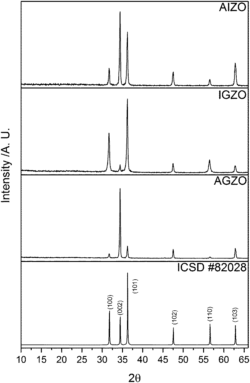 | ||
| Fig. 1 XRD patterns of AGZO, IGZO, and AIZO films deposited via AACVD, using Zn(acac)2 and MCl3 in methanol, at a deposition temperature of 450 °C. A diffraction pattern of ZnO from ICSD #82028 is included for reference. | ||
In a thin film, preferred orientation is often observed in the XRD pattern. This is because the grains cannot be completely randomly oriented as is the case for a powder. For a film, growth is restricted in certain directions, which leads to strain.62 In ZnO, the (002) plane has the lowest surface energy, and hence undoped ZnO films typically show preferred growth in this direction.65,66 The AGZO film also displayed preferred orientation in the (002) plane. This is analogous to AZO and GZO films deposited using the same conditions.36 Conversely, the IGZO film did not display preferred orientation in the (002) plane. Rather, the most intense peaks in its XRD pattern were those corresponding to the (100) and (101) planes. This was analogous to the individually doped IZO films deposited in the same conditions.36 The preferred orientation of the AIZO film appeared to be an amalgamation of the AGZO and IGZO films, with preferred growth in both the (002) and the (101) directions. From these results, it seems evident that the incorporation of aluminium into ZnO promoted growth in the (002) direction, whereas indium promoted growth in the (101) direction. Gallium seems to have had less of an effect over preferred orientation.
In addition, the Scherrer equation was used to estimate the crystallite sizes, from the full-width at half maximum (FWHM) values of the (002) peak for each film:

Elemental analysis
The oxidation states of the elements in the films were determined by XPS. Adventitious carbon was used to calibrate the data, with a binding energy of 285.0 eV for the carbon 1s peaks.70,71 The binding energies of the zinc 2p3/2 and 2p1/2 peaks were consistently found to be 1021.3 eV (±0.2 eV) and 1044.4 eV (±0.2 eV), respectively, which can be attributed to the Zn2+ in ZnO (Fig. 2a and b).72,73 The oxygen 2p peaks for the films could be deconvoluted into three separate peaks, OI, OII, and OIII, with binding energies of 530.0 eV (±0.2 eV), 531.6 eV (±0.2 eV), and 532.6 eV (±0.2 eV), respectively (Fig. 2c and d). OI, the most intense peak, can be attributed to the O2− ions in ZnO.16 OII can be attributed to O2− ions located in oxygen deficient regions in ZnO, and thus relates to the concentration of oxygen vacancies (VO).16,43,55,74,75 OIII can be attributed to surface bound oxygen species, such as O2−, –CO3, and H2O.73,76 Upon etching, the oxygen environments changed, with the relative intensities of the OII and OIII peaks diminishing significantly. This indicates that the surface bound impurities were mostly (but not completely) removed by the etching process. It also suggests that the VO concentration decreased within the bulks of the films. Wong et al. observed that there was a higher concentration of oxygen vacancies at the surfaces of their ZnO nanowires, deposited via CVD.77 They explained this by calculating that VO formation energy is lower near the surface than it is in the bulk. This was confirmed by Deng et al., who also found that VO migration in ZnO is energetically favourable in the direction from the bulk to the surface.78 Carrasco et al. also stated that there is a low diffusion barrier for VO in ZnO.79 These results all agree with our experimental observations.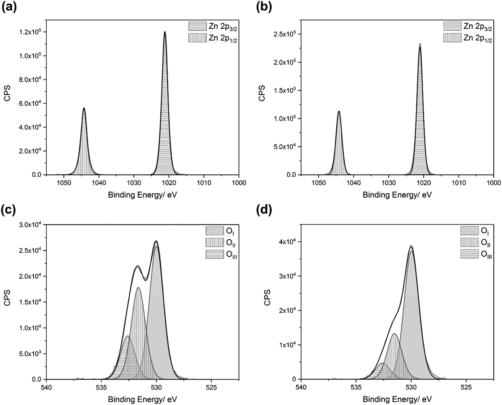 | ||
| Fig. 2 Typical zinc and oxygen XPS spectra for co-doped ZnO, showing the (a) zinc 2p peaks at the surface, (b) zinc 2p peaks in the bulk, (c) oxygen 2p environments at the surface, and (d) oxygen 2p environments in the bulk. Films were deposited via AACVD using Zn(acac)2 and MCl3 in methanol, at a deposition temperature of 450 °C. | ||
All of the dopants were successfully incorporated into the ZnO lattices (Fig. 3). The aluminium 2p3/2 and 2p1/2 peaks had binding energies of 75.1 eV (±0.2 eV) and 75.5 eV (±0.2 eV), respectively, which matches with Al3+ previously reported in AZO films.80 The gallium 3d5/2 and 3d3/2 peaks had binding energies of 20.0 eV (±0.2 eV) and 20.4 eV (±0.2 eV), respectively, which is due to Ga3+.81,82 The indium 3d5/2 and 3d3/2 peaks had binding energies of 444.9 eV (±0.2 eV) and 452.5 eV (±0.2 eV), respectively, which is due to the presence of In3+.83,84 The peaks corresponding to metallic aluminium (72.6 eV),85 metallic gallium (18.7 eV),86 and metallic indium (444.0 eV)87 were not observed.
 | ||
| Fig. 3 Typical dopant XPS spectra for co-doped ZnO, showing the (a) aluminium 2p peaks at the surface, (b) aluminium 2p peaks in the bulk, (c) gallium 3d peaks at the surface, (d) gallium 3d peaks in the bulk, (e) indium 3d peaks at the surface, and (f) indium 3d peaks in the bulk. Films were deposited via AACVD using Zn(acac)2 and MCl3 in methanol, at a deposition temperature of 450 °C. | ||
The dopant:zinc ratios at the film surfaces and within the bulks of the films were also calculated (Table 1). Each dopant was slightly surface-segregated. This is due to the formation of amorphous M2O3 phases at the grain boundaries, caused by the dopants reaching their solubility limit in ZnO.88,89 These oxide phases are insulating, and limit the carrier mobility. Consequently, they result in a deterioration of the electrical properties.90,91 The only exception to this was gallium in the AGZO film, which was bulk-segregated. Another observation that can be made from the XPS data is that, for each film, there appeared to be a preferential incorporation of the lighter dopant elements.
:Zn ratios in the AGZO, IGZO, and AIZO films, as determined by XPS
| Film | Surface concentration/atom% | Bulk concentration/atom% | ||||
|---|---|---|---|---|---|---|
| Dopant | ||||||
| Al | Ga | In | Al | Ga | In | |
| AGZO | 9.6 | 4.2 | — | 9.0 | 4.9 | — |
| IGZO | — | 8.7 | 0.9 | — | 6.3 | 0.8 |
| AIZO | 4.2 | — | 1.8 | 2.1 | — | 1.0 |
Surface morphology
The surface morphologies of the films were highly dopant-dependant (Fig. 4). The grains of the AGZO film were randomly shaped, with their surfaces generally oriented upwards. Moreover, the grains of this film appeared to be smooth and pristine, without any morphological defects such as nano-cracks. The grains of the IGZO film were much more hexagonal in shape. They grew in a columnar fashion, with their surfaces also facing upwards. Jayaraman et al. observed well-defined hexagonal grains in their IGZO films deposited via spray pyrolysis, which had similar diameters to the IGZO grains described in this work.54 The grain structure of the IGZO film is very similar to the GZO film deposited previously using the same conditions.36 In both cases, the grains grew in a similar hexagonal, columnar fashion, with very similar grain sizes. This suggests that gallium has a greater influence over the growth mechanism than indium. The AIZO film had a grain structure that was similar to that of the AGZO film, with randomly shaped grains. Because the AGZO and AIZO films had similar surface morphologies, this also indicates that aluminium had a greater influence over the growth mechanism than indium. The main difference between the AGZO and AIZO morphologies is that the AIZO film had more nano-cracks, which suggests that the use of indium was detrimental towards grain growth. This is likely because indium is the only dopant with an ionic radius larger than Zn2+, resulting in a relatively high concentration of crystal defects, leading to poorer crystal growth.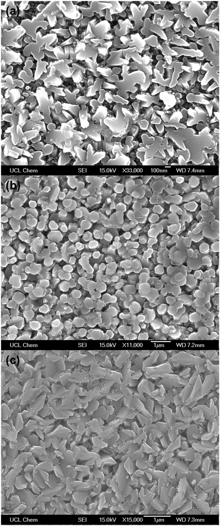 | ||
| Fig. 4 SEM images of the (a) AGZO, (b) IGZO, and (c) AIZO thin films deposited via AACVD, using Zn(acac)2 and MCl3 in methanol, at a deposition temperature of 450 °C. | ||
Large, well-connected grains with few defects are preferable for TCO applications to reduce grain boundary scattering.46,92 Although grain boundary scattering is typically thought to make a smaller contribution towards carrier mobility in samples where the mean free path of the carriers is smaller than the grain size,93 it is important to note that grain boundary scattering has a more profound effect on ZnO-based TCOs than it does on ITO.94 This is because of the higher concentration of trap states at grain boundaries in ZnO-based TCOs compared to ITO.95,96 Therefore, it is important to ensure that the grain structure of doped ZnO has as few morphological defects as possible.
Out of the three films deposited, the AIZO film had the most morphological defects, such as nano-cracks within the grains. This suggests that the presence of Ga3+ resulted in superior grain growth. This is likely due to Ga3+ possessing a similar ionic radius to Zn2+, thus allowing for good quality crystal growth, with relatively few defects in the structure.
Optical properties
For most TCO applications, >80% transmittance in the visible part of the spectrum (400–700 nm) is required.97 The film with the highest visible transmittance was the AGZO film (Fig. 5). The IGZO and AIZO films had very similar transmission profiles. This suggests that the incorporation of indium resulted in an increase in optical absorption, due to the disorder introduced into the structure caused by the large radius of In3+. The disorder results in the formation of localised states near the conduction band minimum. This leads to an increase in the band tail width, known as the Urbach energy.98,99 The additional states that arise due to the structural disorder result in an increase in absorption. Generally, the more disorder that is present in the structure, the greater the Urbach tail width. The use of any dopant will cause some disorder in the structure; however, as indium is the only dopant from this work with an ionic radius larger than that of Zn2+, it will result in the greatest amount of disorder. This explains the reduction in visible transmittance for the films which contain indium. | ||
| Fig. 5 Transmission–reflectance spectra of the AGZO, IGZO, and AIZO films deposited via AACVD, using Zn(acac)2 and MCl3 in methanol, at a deposition temperature of 450 °C. | ||
The transmission–reflectance data was used to generate Tauc plots (Fig. 6). These plots confirm the disorder introduced into the structure due the presence of indium. The Urbach energy typically manifests itself as a long wavelength absorption tail added to the main absorption edge.100 The Urbach tails for the IGZO and AIZO films are higher in terms of absorbance than the AGZO film. The Tauc plots also revealed that the optical band gaps (Eg) of the films were not dopant-dependant, and remained constant at ∼3.27–3.28 eV. In previous work, undoped ZnO deposited in the same conditions yielded a band gap of 3.16 eV.62 Hence, the co-doped films have resulted in a widening of the band gap. This is due to the Burstein–Moss effect, whereby lower energy levels in the conduction band are filled by electrons provided by the dopant elements.101,102 This raises the Fermi level. Hence, because the lower levels are blocked, more energy is required to promote electrons from the valence band to the conduction band.9,29 For this reason, the optical band gap increases.103
 | ||
| Fig. 6 Tauc plots of the co-doped AGZO, IGZO, and AIZO films deposited via AACVD, using Zn(acac)2 and MCl3 in methanol, at a deposition temperature of 450 °C. | ||
Electrical properties
The electrical properties of the films were determined using the van der Pauw technique, and are summarised in Table 2. All of the films were shown to have n-type conductivity, with electrons as the majority charge carrier. The AGZO film displayed the lowest resistivity (1.3 × 10⁻² Ω cm) and highest carrier mobility (7.9 cm2 V−1 s−1). This may indicate that the presence of indium resulted in increased lattice distortion, resulting in poorer transport properties. The AIZO film was close to the AGZO film in terms of mobility, which suggests that the presence of aluminium partially compensated for the lattice distortion caused by indium. This could be due to Al3+ having a smaller ionic radius than Zn2+, whereas In3+ has a larger radius. The IGZO film had the highest resistivity and the lowest mobility, possibly due to the fact that these dopants were the largest in terms of their radii, and hence more lattice distortion would be expected. Additionally, this film possessed smaller grain sizes, which, as previously discussed, could lead to increased grain boundary scattering, particularly for ZnO-based TCOs.| Film | Resistivity × 10−2/Ω cm | Carrier concentration × 1020/cm−3 | Carrier mobility/cm2 V−1 s−1 |
|---|---|---|---|
| AGZO | 1.3 | 1.0 | 7.9 |
| IGZO | 2.1 | 0.7 | 3.3 |
| AIZO | 1.6 | 0.8 | 6.8 |
The resistivity values of these films are higher than the most conductive individually doped film (10 mol% AZO) which was deposited previously in the same conditions.36 This could be because the total amount of dopant incorporated into the co-doped films (as indicated by XPS) was less than the total amount of dopant incorporated for the most conductive individually doped AZO film. As a result, a lower carrier concentration had been supplied to the conduction band, leading to higher resistivity.
Nguyen et al. reported that the resistivity of their GZO film (4.4 × 10⁻⁴ Ω cm) was lower than the resistivity of their IGZO film (9.0 × 10⁻⁴ Ω cm), both deposited via magnetron sputtering.55 They explained that this was due to the lower crystallinity of the IGZO film, which led to an increase in localized states in the band structure, which subsequently acted as electron traps. Additionally, the different electronegativity values of gallium (1.81) and indium (1.78) indicate that electrons will experience a randomly fluctuating potential, which can lead to a lower carrier mobility.
The optoelectronic properties of the materials in this work are comparable or superior to several previous attempts at co-doped ZnO. Ebrahimifard et al. synthesised AGZO thin films on glass substrates via dip coating, and varied the concentrations of aluminium and gallium.104 Their minimum resistivity value was on the order of 100 Ω cm. Park et al. deposited AGZO nanofibers films via electrospinning, and obtained a minimum resistivity on the order of 102 Ω cm.105 Jayaraman et al. deposited IGZO thin films on glass substrates via spray pyrolysis – a technique which is closely related to AACVD. They achieved a minimum resistivity of 1.1 × 10⁻² Ω cm, which is similar to the films from this work.
While co-doped ZnO films with lower resistivity values (ca. 10−4 Ω cm) have been prepared previously via PLD106 and magnetron sputtering,107 the ease of deposition using AACVD make the films from this work especially promising, and with the optimisation of deposition conditions, further improvements in the optoelectronic properties are achievable.
Conclusions
AGZO, IGZO, and AIZO thin films were deposited via AACVD for the first time. All of the films were pure wurtzite ZnO, with no secondary phases observed. The preferred orientation of the films was also shown to be dopant-dependant. The incorporation of aluminium promoted growth in the (002) direction, whereas indium promoted growth in the (101) direction. XPS analysis confirmed the presence of the oxidised dopants in each film. The morphologies of the films were dopant-dependant, and the presence of gallium appeared to result in superior grain growth. This is likely because the ionic radius of gallium is closer to Zn2+ than the other dopants, leading to higher quality crystal growth. Using indium was detrimental towards grain growth due to its large ionic radius, which caused increased crystal disorder. This disorder was observable in the transmission–reflectance spectra of the IGZO and AIZO films, and caused a higher absorbance in the visible part of the spectrum. This was confirmed by the more significant Urbach tails in the Tauc plots for the IGZO and AIZO films. The AGZO film was the most conductive, due to the high-quality crystallinity and morphology, which led to superior transport properties.Conflicts of interest
There are no conflicts to declare.Acknowledgements
The authors would like to thank the EPSRC for grant EP/L017709 and UCL for an impact studentship (D. B. P.), as well as NSG (Pilkington Technology Management Limited, European Technical Centre, Hall Lane, Lathom, Nr. Ormskirk, L40 5UF, UK) for their support.References
- S. C. Dixon, D. O. Scanlon, C. J. Carmalt and I. P. Parkin, J. Mater. Chem. C, 2016, 419, 6946–6961 RSC.
- J. L. Zhao, X. W. Sun, H. Ryu and Y. B. Moon, Opt. Mater., 2011, 33, 768–772 CrossRef CAS.
- J. Clatot, G. Campet, A. Zeinert, C. Labrugère, M. Nistor and A. Rougier, Sol. Energy Mater. Sol. Cells, 2011, 95, 2357–2362 CrossRef CAS.
- U.S. Geological Survey, Miner. Commod. Summ., 2017, p. 202 Search PubMed.
- A. Janotti and C. G. Van de Walle, Rep. Prog. Phys., 2009, 72, 126501 CrossRef.
- S. J. Pearton, D. P. Norton, K. Ip, Y. W. Heo and T. Steiner, Superlattices Microstruct., 2003, 34, 3–32 CrossRef CAS.
- Ü. Özgür, Y. I. Alivov, C. Liu, A. Teke, M. A. Reshchikov, S. Doǧan, V. Avrutin, S. J. Cho and H. Morko, J. Appl. Phys., 2005, 98, 1–103 CrossRef.
- M. R. Waugh, G. Hyett and I. P. Parkin, Chem. Vap. Deposition, 2008, 14, 366–372 CrossRef CAS.
- A. Jain, P. Sagar and R. M. Mehra, Solid-State Electron., 2006, 50, 1420–1424 CrossRef CAS.
- N. Kamarulzaman, M. F. Kasim and R. Rusdi, Nanoscale Res. Lett., 2015, 10, 346 CrossRef PubMed.
- C. H. Lee and D. W. Kim, J. Electroceram., 2014, 33, 12–16 CrossRef CAS.
- R. Nasser, W. Ben, H. Othmen, H. Elhouichet and M. Férid, Appl. Surf. Sci., 2017, 393, 486–495 CrossRef CAS.
- N. Rashidi, V. L. Kuznetsov, J. R. Dilworth, M. Pepper, P. J. Dobson and P. P. Edwards, J. Mater. Chem. C, 2013, 1, 6960 RSC.
- E. Fortunato, V. Assunção, A. Gonçalves, A. Marques, H. Águas, L. Pereira, I. Ferreira, P. Vilarinho and R. Martins, Thin Solid Films, 2004, 451–452, 443–447 CrossRef CAS.
- Y. H. Kim, J. Jeong, K. S. Lee, J. K. Park, Y. J. Baik, T. Y. Seong and W. M. Kim, Appl. Surf. Sci., 2010, 256, 5102–5107 CrossRef CAS.
- C.-F. Yu, S.-H. Chen, S.-J. Sun and H. Chou, Appl. Surf. Sci., 2011, 257, 6498–6502 CrossRef CAS.
- Z. C. Jin, I. Hamberg and C. G. Granqvist, J. Appl. Phys., 1988, 64, 5117–5131 CrossRef CAS.
- M. Kon, P. K. Song, Y. Shigesato, P. Frach, A. Mizukami and K. Suzuki, Jpn. J. Appl. Phys., 2002, 41, 814–819 CrossRef CAS.
- D. L. Zhu, Q. Wang, S. Han, P. J. Cao, W. J. Liu, F. Jia, Y. X. Zeng, X. C. Ma and Y. M. Lu, Appl. Surf. Sci., 2014, 298, 208–213 CrossRef CAS.
- K. Djessas, I. Bouchama, J. L. Gauffier and Z. B. Ayadi, Thin Solid Films, 2014, 555, 28–32 CrossRef CAS.
- P. Gondoni, M. Ghidelli, F. Di Fonzo, V. Russo, P. Bruno, J. Martí-Rujas, C. E. Bottani, A. Li Bassi and C. S. Casari, Thin Solid Films, 2012, 520, 4707–4711 CrossRef CAS.
- S.-M. Park, T. Ikegami and K. Ebihara, Thin Solid Films, 2006, 513, 90–94 CrossRef CAS.
- G. Socol, D. Craciun, I. N. Mihailescu, N. Stefan, C. Besleaga, L. Ion, S. Antohe, K. W. Kim, D. Norton, S. J. Pearton, A. C. Galca and V. Craciun, Thin Solid Films, 2011, 520, 1274–1277 CrossRef CAS.
- T. Ohgaki, Y. Kawamura, T. Kuroda, N. Ohashi, Y. Adachi, T. Tsurumi, F. Minami and H. Haneda, Key Eng. Mater., 2003, 248, 91–94 CrossRef CAS.
- C.-Y. Chen, L.-H. Hsiao and J.-I. Chyi, J. Cryst. Growth, 2015, 425, 216–220 CrossRef CAS.
- H. Saarenpää, T. Niemi, A. Tukiainen, H. Lemmetyinen and N. Tkachenko, Sol. Energy Mater. Sol. Cells, 2010, 94, 1379–1383 CrossRef.
- W. J. Maeng and J.-S. Park, J. Electroceram., 2013, 31, 338–344 CrossRef CAS.
- P. R. Chalker, P. A. Marshall, S. Romani, J. W. Roberts, S. J. C. Irvine, D. A. Lamb, A. J. Clayton and P. A. Williams, J. Vac. Sci. Technol., A, 2013, 31, 01A120 Search PubMed.
- H. Hung-Chun Lai, T. Basheer, V. L. Kuznetsov, R. G. Egdell, R. M. J. Jacobs, M. Pepper and P. P. Edwards, J. Appl. Phys., 2012, 112, 83708 CrossRef.
- S. Edinger, N. Bansal, M. Bauch, R. A. Wibowo, G. Ujvari, R. Hamid, G. Trimmel and T. Dimopoulos, J. Mater. Sci., 2017, 52, 8591–8602 CrossRef CAS.
- J. Hu and R. G. Gordon, J. Appl. Phys., 1992, 71, 880–890 CrossRef CAS.
- T. Terasako, Y. Ogura, K. Ohmae, S. Fujimoto, M. Yagi and S. Shirakata, Surf. Coat. Technol., 2013, 230, 245–253 CrossRef CAS.
- J. Nishino, T. Kawarada, S. Ohshio, H. Saitoh, K. Maruyama and K. Kamata, J. Mater. Sci. Lett., 1997, 16, 2887–2890 CrossRef.
- D. S. Bhachu, G. Sankar and I. P. Parkin, Chem. Mater., 2012, 24, 4704–4710 CrossRef CAS.
- J. A. Manzi, C. E. Knapp, I. P. Parkin and C. J. Carmalt, Thin Solid Films, 2016, 616, 477–481 CrossRef CAS.
- D. B. Potter, D. S. Bhachu, M. J. Powell, J. A. Darr, I. P. Parkin and C. J. Carmalt, Phys. Status Solidi, 2016, 7, 1346–1352 CrossRef.
- A. A. Yaroshevsky, Geochem. Int., 2006, 44, 48–55 CrossRef.
- A. Nebatti, C. Pflitsch, B. Curdts and B. Atakan, Mater. Sci. Semicond. Process., 2015, 39, 467–475 CrossRef CAS.
- A. Abrutis, L. Silimavicius, V. Kubilius, T. Murauskas, Z. Saltyte and V. Plausinaitiene, Thin Solid Films, 2015, 576, 88–97 CrossRef CAS.
- S. Kuprenaite, T. Murauskas, A. Abrutis, V. Kubilius, Z. Saltyte and V. Plausinaitiene, Surf. Coat. Technol., 2014, 271, 156–164 CrossRef.
- P. K. Jain and M. Salim, Mater. Res. Express, 2017, 4, 75902 CrossRef.
- B. Onwona-Agyeman, M. Nakao, T. Kohno, D. Liyanage, K. Murakami and T. Kitaoka, Chem. Eng. J., 2013, 219, 273–277 CrossRef CAS.
- J. H. Lim, S. M. Lee, H.-S. Kim, H. Y. Kim, J. Park, S.-B. Jung, G. C. Park, J. Kim and J. Joo, Sci. Rep., 2017, 7, 41992 CrossRef CAS PubMed.
- H. Wang, S. Baek, J. Song, J. Lee and S. Lim, Nanotechnology, 2008, 19, 75607 CrossRef PubMed.
- H. J. Ko, Y. F. Chen, S. K. Hong, H. Wenisch, T. Yao and D. C. Look, Appl. Phys. Lett., 2000, 77, 3761 CrossRef CAS.
- J. Nomoto, M. Konagai, T. Miyata and T. Minami, J. Vac. Sci. Technol., A, 2010, 28, 861 CAS.
- R. D. Shannon and C. T. Prewitt, Acta Crystallogr., Sect. B: Struct. Crystallogr. Cryst. Chem., 1970, 26, 1046–1048 CrossRef CAS.
- V. Assunção, E. Fortunato, A. Marques, H. Águas, I. Ferreira, M. E. V. Costa and R. Martins, Thin Solid Films, 2003, 427, 401–405 CrossRef.
- K.-W. Seo, H.-S. Shin, J.-H. Lee, K.-B. Chung and H.-K. Kim, Vacuum, 2014, 101, 250–256 CrossRef CAS.
- O. Makuku, F. Mbaiwa and T. S. Sathiaraj, Ceram. Int., 2016, 42, 14581–14586 CrossRef CAS.
- V. K. Jayaraman, A. M. Álvarez, Y. M. Kuwabara, Y. Koudriavstev and M. D. L. L. O. Amador, Mater. Sci. Semicond. Process., 2016, 47, 32–36 CrossRef CAS.
- C. M. Hsu, W. C. Tzou, C. F. Yang and Y. J. Liou, Materials, 2015, 8, 2769–2781 CrossRef.
- H. Q. Le and S. J. Chua, J. Phys. D: Appl. Phys., 2011, 44, 125104 CrossRef.
- V. K. Jayaraman, A. M. Alvarez and M. d. l. l. O. Amador, Phys. E, 2017, 86, 164–167 CrossRef CAS.
- N. H. Nguyen Tran, H. T. Nguyen, Y.-R. Liu, M. Aminzare, A. T. T. Pham, S. Cho, D. P. Wong, K.-H. Chen, T. Seetawan, N. K. Pham, H. K. T. Ta, C. V. Tran and T. B. Phan, ACS Appl. Mater. Interfaces, 2016, 8, 33916–33923 Search PubMed.
- S. Teehan, H. Efstathiadis and P. Haldar, J. Alloys Compd., 2011, 509, 1094–1098 CrossRef CAS.
- T. Tohsophon, N. Wattanasupinyo, B. Silskulsuk and N. Sirikulrat, Thin Solid Films, 2011, 520, 726–729 CrossRef CAS.
- V. K. Jayaraman, A. Maldonado-Alvarez, A. E. Jimenez-Gonzalez and M. D. L. L. Olvera-Amador, Mater. Lett., 2016, 181, 52–55 CrossRef CAS.
- X. Hou and K.-L. Choy, Chem. Vap. Deposition, 2006, 12, 583–596 CrossRef CAS.
- P. Marchand, I. A. Hassan, I. P. Parkin and C. J. Carmalt, Dalton Trans., 2013, 42, 9406–9422 RSC.
- M. J. Powell, D. B. Potter, R. L. Wilson, J. A. Darr, I. P. Parkin and C. J. Carmalt, Mater. Des., 2017, 129, 116–124 CrossRef CAS.
- D. B. Potter, M. J. Powell, J. A. Darr, I. P. Parkin and C. J. Carmalt, RSC Adv., 2017, 7, 10806–10814 RSC.
- A. Kafizas, N. Noor, P. Carmichael, D. O. Scanlon, C. J. Carmalt and I. P. Parkin, Adv. Funct. Mater., 2014, 24, 1758–1771 CrossRef CAS.
- R. Wang, L. L. H. King and A. W. Sleight, J. Mater. Res., 2011, 11, 1659–1664 CrossRef.
- N. Fujimura, T. Nishihara, S. Goto, J. Xu and T. Ito, J. Cryst. Growth, 1993, 130, 269–279 CrossRef CAS.
- M. Birkholz, Phys. Rev. B: Condens. Matter Mater. Phys., 2003, 68, 1–8 CrossRef.
- S. C. Dixon, S. Sathasivam, B. A. D. Williamson, D. O. Scanlon, C. J. Carmalt and I. P. Parkin, J. Mater. Chem. C, 2017, 5, 7585–7597 RSC.
- M. A. Ehsan, H. N. Ming, M. Misran, Z. Arifin, E. R. T. Tiekink, A. P. Safwan, M. Ebadi, W. J. Basirun and M. Mazhar, Chem. Vap. Deposition, 2012, 18, 191–200 CrossRef CAS.
- M. Ohyama, H. Kozuka and T. Yoko, J. Am. Ceram. Soc., 2005, 81, 1622–1632 CrossRef.
- S. Basharat, C. J. Carmalt, R. Binions, R. Palgrave and I. P. Parkin, Dalton Trans., 2008, 591–595 RSC.
- S. Basharat, C. J. Carmalt, S. A. Barnett, D. A. Tocher and H. O. Davies, Inorg. Chem., 2007, 46, 9473–9480 CrossRef CAS PubMed.
- S. Karamat, R. S. Rawat, P. Lee, T. L. Tan and R. V. Ramanujan, Prog. Nat. Sci.: Mater. Int., 2014, 24, 142–149 CrossRef CAS.
- A. Gulino, I. Fragala, S. Chimiche and V. A. Doria, Chem. Mater., 2002, 14, 116–121 CrossRef CAS.
- H. Jung, D. Kim and H. Kim, Appl. Surf. Sci., 2014, 297, 125–129 CrossRef CAS.
- S. Chirakkara and S. B. Krupanidhi, Phys. Status Solidi RRL, 2012, 6, 34–36 CrossRef CAS.
- D. J. Goyal, C. Agashe, M. G. Takwale, V. G. Bhide, S. Mahamuni and S. K. Kulkarni, J. Mater. Res., 1993, 8, 1052–1056 CrossRef CAS.
- K. Mun Wong, S. M. Alay-E-Abbas, Y. Fang, A. Shaukat and Y. Lei, J. Appl. Phys., 2013, 114, 034901 CrossRef.
- B. Deng, A. Luisa da Rosa, T. Frauenheim, J. P. Xiao, X. Q. Shi, R. Q. Zhang and M. A. Van Hove, Nanoscale, 2014, 6, 11882–11886 RSC.
- J. Carrasco, N. Lopez and F. Illas, Phys. Rev. Lett., 2004, 93, 3–6 CrossRef PubMed.
- D. S. Y. Jayathilake, T. A. N. Peiris, J. Sagu, D. B. Potter, K. G. U. Wijayantha, C. J. Carmalt and D. J. Southee, ACS Sustainable Chem. Eng., 2017, 5, 4820–4829 CrossRef CAS.
- R. Carli and C. L. Bianchi, Appl. Surf. Sci., 1994, 74, 99–102 CrossRef CAS.
- G. Cossu, G. M. Ingo, G. Mattogno, G. Padeletti and G. M. Proietti, Appl. Surf. Sci., 1992, 56–58, 81–88 CrossRef CAS.
- A. W. C. Lin, N. R. Armstrong and T. Kuwana, Anal. Chem., 1977, 49, 1228–1235 CrossRef CAS.
- L. L. Kazmerski, O. Jamjoum, P. J. Ireland and S. K. Deb, J. Vac. Sci. Technol., 1981, 19, 467–471 CrossRef CAS.
- R. Hauert, J. Patscheider, M. Tobler and R. Zehringer, Surf. Sci., 1993, 292, 121–129 CrossRef CAS.
- S. Evans, Surf. Interface Anal., 1985, 7, 299–302 CrossRef CAS.
- G. Hollinger, R. Skheyta-Kabbani and M. Gendry, Phys. Rev. B: Condens. Matter Mater. Phys., 1994, 49, 11159–11167 CrossRef CAS.
- M. Miki-Yoshida, F. Paraduay-Delgado, Q. Estrada-Lopez and E. Andrade, Thin Solid Films, 2000, 376, 99–109 CrossRef CAS.
- S. S. Shinde, P. S. Shinde, S. M. Pawar, A. V. Moholkar, C. H. Bhosale and K. Y. Rajpure, Solid State Sci., 2008, 10, 1209–1214 CrossRef CAS.
- J.-H. Lee and B.-O. Park, Thin Solid Films, 2003, 426, 94–99 CrossRef CAS.
- Y. Shigesato, S. Takaki and T. Haranoh, J. Appl. Phys., 1992, 71, 3356–3364 CrossRef CAS.
- J.-H. Kim and S.-M. Koo, Ceram. Int., 2015, 41, 37–42 CrossRef CAS.
- K. G. Saw, N. M. Aznan, F. K. Yam, S. S. Ng and S. Y. Pung, PLoS One, 2015, 10, 1–17 Search PubMed.
- H. Liu, V. Avrutin, N. Izyumskaya, Ü. Özgr and H. Morkoç, Superlattices Microstruct., 2010, 48, 458–484 CrossRef CAS.
- K. Ellmer and R. Mientus, Thin Solid Films, 2008, 516, 5829–5835 CrossRef CAS.
- K. Ellmer and R. Mientus, Thin Solid Films, 2008, 516, 4620–4627 CrossRef CAS.
- D. S. Bhachu, M. R. Waugh, K. Zeissler, W. R. Branford and I. P. Parkin, Chem. – Eur. J., 2011, 17, 11613–11621 CrossRef CAS PubMed.
- S. Schönau, F. Ruske, S. Neubert and B. Rech, Appl. Phys. Lett., 2013, 103, 192108 CrossRef.
- A. S. Hassanien and A. A. Akl, J. Alloys Compd., 2015, 648, 280–290 CrossRef CAS.
- F. Mozer and F. Urbach, Phys. Rev., 1956, 102, 1519–1523 CrossRef.
- E. Burstein, Phys. Rev., 1954, 93, 632–633 CrossRef CAS.
- T. S. Moss, Proc. Phys. Soc., London, Sect. B, 1954, 67, 775–782 CrossRef.
- S. Jin, Y. Yang, J. E. Medvedeva, J. R. Ireland, A. W. Metz, J. Ni, C. R. Kannewurf, A. J. Freeman and T. J. Marks, J. Am. Chem. Soc., 2004, 126, 13787–13793 CrossRef CAS PubMed.
- R. Ebrahimifard, M. R. Golobostanfard and H. Abdizadeh, Appl. Surf. Sci., 2014, 290, 252–259 CrossRef CAS.
- M. Park and S. M. Han, Thin Solid Films, 2015, 590, 307–310 CrossRef CAS.
- S. Jin-Hyun, S. Dong-Kyun, L. HeeYoung, L. Jai-Yeoul, C. Nam-In and L. Se-Jong, J. Korean Phys. Soc., 2009, 55, 947 CrossRef.
- S.-C. Chang, Int. J. Photoenergy, 2014, 2014, 1–6 CAS.
| This journal is © The Royal Society of Chemistry 2018 |