
Degradation of encapsulated perovskite solar cells driven by deep trap states and interfacial deterioration†
Dhruba B.
Khadka
 *ab,
Yasuhiro
Shirai
*a,
Masatoshi
Yanagida
a and
Kenjiro
Miyano
a
*ab,
Yasuhiro
Shirai
*a,
Masatoshi
Yanagida
a and
Kenjiro
Miyano
a
aGlobal Research Center for Environment and Energy based on Nanomaterials Science (GREEN), National Institute for Materials Science (NIMS), 1-1 Namiki, Tsukuba, Ibaraki 305-0044, Japan. E-mail: KHADKA.B.Dhruba@nims.go.jp; SHIRAI.Yasuhiro@nims.go.jp
bInternational Center for Young Scientists (ICYS), National Institute for Materials Science (NIMS), 1-1 Namiki, Tsukuba, Ibaraki 305-0044, Japan
First published on 28th November 2017
Abstract
The degradation of encapsulated perovskite devices has been investigated by optoelectronic characterization. The performance of the encapsulated device dropped by approximately 50% of the initial value after five months. The degradation of device performance was found to be influenced by both interface recombination and deep trap assisted recombination in the perovskite. The analysis of temperature dependent current–voltage characteristics and capacitance spectra revealed that the decrease in the activation energy of interface recombination, deepening of the defect levels and reduction in the diffusion potential of devices led to deterioration of device parameters with aging. The degradation of the encapsulated device might be governed by dissociation and migration of constituent ions which induce deeper defect levels in the perovskite layer and deteriorate the interface with aging.
1. Introduction
Perovskite solar cells (PSCs) have drawn enormous attention due to the rapid improvement in device efficiency (∼22%) showing a competitive performance to silicon and chalcopyrite based photovoltaic devices.1–3 Although perovskite devices demonstrated startling performance based on various fabrication methods3–7 and device architectures with a number of carrier transport materials (CTMs),8–10 the poor stability of devices has been the most problematic issue for commercialization.3,11–14 Indeed, the improvement in device stability has been attempted in terms of device structures,15,16 engineering CTMs,8,17,18 electrodes11 and coating with hydrophobic materials.19,20 The degradation of PSCs is reported to be accelerated by external factors such as humidity,15,21,22 UV light,23,24 temperature21,22 and oxygen21 coupled with intrinsic properties of perovskite materials:21,25,26 chemical instability, ion migration, dissociation of constituents and worsening of the carrier transport layer (CTL) and external contacts.21,22,27,28 Identifying the mechanisms behind the degradation is crucial to resolve the big hurdle of short lifespan of perovskite devices.Let us go into some details of the degradation studies quoted above. The atmospheric moisture has been regarded as the main cause of irreversible degradation of perovskite material.13,21,29,30 Yang et al. investigated the degradation mechanism under controlled humidity using in situ techniques.31 They observed rapid degradation of the perovskite film under higher humidity and formation of a new hydrated compound. Choi and co-workers32 reported that the moisture-induced irreversible degradation of perovskite material is triggered by trapped charges at the grain boundaries. In addition, they also observed the synergetic effect of oxygen on degradation. Note that degradation of the perovskite film may be influenced by the carrier transport layers8,17 and the contact electrode,11,33 which could make the study of separate perovskite films insufficient. A study by Bryant et al. found that light- and oxygen-induced degradation leads to low operational stability of perovskite devices exposed to ambient conditions.34 They suggested that the operational stability can be critically improved by protecting perovskite with an oxygen-impermeable interlayer. Although the device stability improved for encapsulated devices22,24 or devices kept in a nitrogen atmosphere,3,28,33 they also suffered significant degradation with aging. This indicates that there are intrinsic factors for degradation of perovskite devices induced with aging. Cheng and co-workers carried out a post-mortem analysis of encapsulated perovskite devices (significantly degraded) after prolonged aging at high temperature and humidity.22 They observed less severe and slow degradation but the perovskite still decomposed into HI and CH3NH2 gases. It is found that the saturated gases that are released cause voids at the interface and corrode the metal contact leading to deterioration of device parameters. Guerrero et al. also reported that interfacial deterioration caused by the reaction between the metal electrode and perovskite could result in degradation of the device in the absence of moisture.28 Interestingly, Besleaga et al. suggested that iodine is dislocated by the electric field between the electrodes which causes iodine migration.33 This results in intrinsic degradation of the device. A recent study by Zhang et al. reported that the ion migration accelerated degradation of PSCs at the device level.27 They observed not only diffusion of mobile iodide from perovskite into CTLs and the contact electrode but also diffusion of the electrode metal atom/ions into the perovskite. Song et al. suggested that increased trap states at the surface of perovskite induced performance degradation of PSCs, based on the J–V characteristics and open circuit voltage decay measurements.35 Moreover, theoretical studies postulated that the interfacial ionic migration and formation of defects such as antisites (MAPb, PbMA, MAI, PbI, IPb), interstitials (MAi, Pbi, Xi) and vacancies (VMA, VPb, VI) can deteriorate the optoelectronic quality of the perovskite layer and also induce interface degradation leading to dominant effects on device performance.36–38 Therefore, systematic studies are necessary to correlate the degradation of device performance with the perovskite material properties: chemical decomposition, ionic migration, optophysical/optoelectronic properties, and interfacial interactions.
In this study, we have investigated the degradation of encapsulated devices focusing on optoelectronic characterization: photocurrent–voltage characteristics and admittance spectra. The degradation of device performance was found to be dominated by interface recombination (decrease in EA ∼ 1.40 eV to ≤1 eV) and formation of deeper defect states (∼0.3 to 0.8 eV). The device simulations were also carried out using SCAPS (solar cell capacitor simulator). The degraded device characteristics were reproduced by adjusting the simulation parameters according to the optoelectronic measurements, which supports our interpretation.
2. Experimental section
Materials and preparation
All chemicals were purchased from commercial suppliers as mentioned, and unless otherwise specified, they were used as received. Methylammonium iodide (MAI) and methylammonium chloride (MACl) were of battery grade from Wako chemical company. The PbI2–DMSO complex was prepared following the report by Seok and co-workers.39 In brief, PbI2 (50 g) was dissolved in DMSO (150 ml) at 60 °C. After that, toluene (350 ml) was slowly added into the PbI2 solution and the precipitation (PbI2–(DMSO)2) was filtered and dried for 3 h at room temperature. The PbI2–(DMSO)2 complex was reduced to PbI2–DMSO by further annealing the precipitation for 24 h in a vacuum oven at 60 °C. For the fabrication of perovskite films, the precursor solution was prepared by dissolving the PbI2–DMSO complex and methylammonium iodide (MAI) + methylammonium chloride (MACl) in anhydrous DMF (500 mg ml−1) and ethanol (50 mg ml−1; 19![[thin space (1/6-em)]](https://www.rsc.org/images/entities/char_2009.gif) :1 ratio, by mass), respectively. [6,6]-Phenyl C61 butyric acid methyl ester (PC61BM) [Sigma Aldrich, 99% purity] solution (2 wt%) dissolved in anhydrous chlorobenzene (CB) was used for coating of the electron transport layer (ETL). Tetrabutylammonium iodide (TBAI) (Sigma Aldrich, 99% purity) precursor solution (0.01 wt%) was prepared by dissolving in ethanol for doping of the PCBM surface.40 All the solutions were filtered using 0.45 μm syringe filters to avoid the risk of unwanted particles in the precursor solution.
:1 ratio, by mass), respectively. [6,6]-Phenyl C61 butyric acid methyl ester (PC61BM) [Sigma Aldrich, 99% purity] solution (2 wt%) dissolved in anhydrous chlorobenzene (CB) was used for coating of the electron transport layer (ETL). Tetrabutylammonium iodide (TBAI) (Sigma Aldrich, 99% purity) precursor solution (0.01 wt%) was prepared by dissolving in ethanol for doping of the PCBM surface.40 All the solutions were filtered using 0.45 μm syringe filters to avoid the risk of unwanted particles in the precursor solution.
Device fabrication
We employed the low temperature solution process method to fabricate the planar heterojunction PSCs. First, the ITO substrates were pre-cleaned in an ultrasonic bath with detergent, pure water, and 2-propanol, followed by ultraviolet-ozone treatment for 5 min to remove the organic residues. A thin HTM layer (30 nm) of poly(3,4-ethylenedioxythiophene):poly(styrene sulfonate) (PEDOT:PSS, Clevios, Al4083) was deposited by spin coating at 3000 rpm and subsequently dried at 130 °C for 10 min on a hot plate in air. Then the substrates were transferred into a nitrogen-filled glove box (<1.0 ppm O2 and H2O) and the rest of the steps were carried out inside the glove box. PbI2 precursor solution was spin coated at 3000 rpm for 90 s and a mixed precursor solution of MAI + MACl was subsequently spun on to the PbI2 layer at 4000 rpm, for 30 s. Then the as-grown CH3NH3PbI3−xClx perovskite films were crystallized simply by placing them on a hot plate either with MACl powder in a Petri dish or without MACl powder at 100 °C. For the ETM layer, PC61BM was deposited on top of the perovskite films at 700 rpm for 30 s and subsequently at 5000 rpm for 10 s, followed by deposition of a thin TBAI layer spun at 3000 rpm for 25 s. Note that the device fabricated with MACl treatment is denoted as device-I and that without MACl treatment is denoted as device-II. To complete the device structure, the samples were transferred into the evaporation chamber connected to the glove box for metal contact deposition. 100 nm of Ag was thermally evaporated at a base pressure of <10−4 Pa to obtain complete devices with an area of ∼0.26 cm2. Then, all the devices were sealed using a UV-curable resin (UV RESIN XNR5516Z; Nagase ChemeteX, Japan) inside the glove box before the subsequent measurements in ambient conditions. For encapsulation, the perovskite device was covered with a transparent plastic well fitted to device size which was glued using a UV-curable resin. The device encapsulation was completed by baking the sealed device under UV-light for 5 min.Device characterization
The current density–voltage (J–V) characteristics and spectral responses (external quantum efficiency (EQE), internal quantum efficiency (IQE) and reflectance spectra) were characterized using a spectrometer (SM-250, RU-60 with integrated sphere, Bunko Keiki, Japan). The capacitance–frequency (C–f) response was measured using an LCR meter (E4980A, Agilent), which probes from 20 Hz to 2 MHz at an ac voltage amplitude of 10 mV under dark conditions in the temperature range of 253–343 K, whereas capacitance–voltage (C–V) measurements were carried out at 1 kHz. For temperature dependent characterization, we used a temperature controlled chamber (SU-221) having a control error of ±0.1 K (°C).3. Results and discussion
We chose two types of encapsulated perovskite solar cells (PSCs) of device structure ITO/PEDOT:PSS/perovskite/PCBM/TBAI/Ag (Fig. S1, ESI†): (a) device-I having the best PCE in the range of η ∼ 14–15% and (b) device-II having the best PCE in the range of η = 11–12%. As stated earlier, device-I was fabricated with MACl treatment and device-II without. The details of device characterization have been discussed in our previous report.6 Two types of devices (better and lower initial quality, respectively) were intentionally chosen in order to see if the mode of degradation depends on the initial quality. The difference between the two was presumed to be due to the bulk crystallinity of the perovskite layer. We analysed the J–V characteristics and capacitance spectroscopy of fresh and degraded devices.3.1. Device degradation and electrical properties
Fig. 1a depicts the J–V curves of encapsulated perovskite devices degraded with aging. Those devices were stored under ambient conditions and measurements were carried out periodically under standard conditions (one sun illumination, AM 1.5G at room temperature). The device parameters are summarized in Table 1. We observed a noticeable drop in open circuit voltage (VOC) rather than short circuit current (JSC) during the first three months. The performance of our devices dropped by approximately fifty percent of the initial PCE after five months. The perovskite devices without encapsulation degraded much faster due to various external factors.21,22,35 The degradation trends of device parameters with aging are summarized in ESI† (Fig. S2 and Table S1). Note that we tested J–V characteristics (Fig. S3, ESI†) of the encapsulated device under standard testing conditions (one sun illumination, AM 1.5G) by varying the relative humidity (30–90%) for confirmation of encapsulation. No noticeable variation was observed in the figures of merit of the device even in a severe humid environment. This indicates that internal factors are the primary cause for degradation. Multiple reports suggested that ion migration in the device results in interfacial worsening and deterioration of the perovskite layer which accelerates degradation.27,28,33 | ||
| Fig. 1 J–V characteristics of perovskite solar cells (device-I) after aging for different time intervals (a). Diode ideality factor (A) and reverse saturation current density (J0) (b) of the perovskite devices extracted from the analysis of respective J–V curves. | ||
| Device perforamnce/days | Device-I | |||
|---|---|---|---|---|
| J SC (mA cm−2) | V OC (V) | FF (%) | η (%) | |
| 0 | 20.12 | 0.95 | 79.81 | 15.09 |
| 90 | 19.93 | 0.89 | 78.47 | 13.33 |
| 120 | 16.48 | 0.79 | 76.79 | 10.12 |
| 150 | 15.56 | 0.62 | 70.15 | 6.71 |
To understand the degradation kinetics of perovskite devices, we extracted the electrical parameters, diode ideality factor (A) and reverse saturation current density (J0), which are related to defect activities in the devices,41–43 by fitting with the diode equation.43
 | (1) |
The changes in the spectral response with aging (Fig. S5, ESI†) revealed a significant loss in EQE in the range of 300–730 nm which indicates inefficient carrier collection. It is attributed to the degradation of the perovskite layer and deterioration of the interfacial carrier transport layer.43,44 The higher values of A and J0 with aging signify that the degradation of device performances is attributed to increased trap assisted recombination phenomena.41–43 This could be due to either the intrinsic instability of perovskite material, the ill-behaved interface at CTLs, or intra-layer ion migration in the perovskite device.22,27,28 We will discuss some of these below.
To investigate the impact of aging on the interface layer quality and recombination mechanism, the temperature dependent J–V characteristics were studied in the temperature range of 233 to 353 K. The temperature range was chosen to avoid the phase transition of the perovskite crystal.45 The temperature dependence of device parameters, particularly, VOCvs. T, provides insight into the dominant recombination processes and the effect of the defect/trap level that lowers VOC. Fig. 2 depicts temperature dependency of VOC of fresh and degraded devices. The observed trends are in good agreement with other reports.46–50 The activation energy (EA) of the dominant recombination can be estimated by linear extrapolation of the VOC–T plots to 0 K as given by the equation43
 | (2) |
 | ||
| Fig. 2 The temperature dependent open circuit voltage (VOC–T) of the fresh device (a) and the degraded device (b). Plots of the trend of efficiency (η) (c) and VOC (d) of fresh and aged devices with activation energy of interface recombination (EA). | ||
3.2. Admittance spectroscopy and instability impact
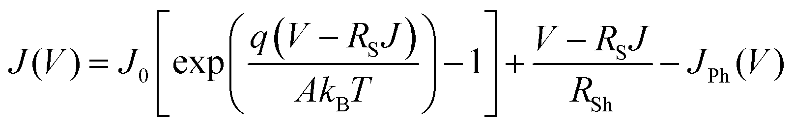
Admittance spectroscopy (AS) is commonly employed to extract the carrier profile, distribution of defect density and energetic position of the defects within the band gap by tracking the capacitance response from the absorber layer.51,52 Through the AS technique, the degradation phenomena are further elucidated. We analyzed the capacitance voltage (C–V) scans of devices as depicted in Fig. 3. The Mott–Schottky plot (Fig. 3a) shows full depletion in the well confined p-i-n junction. Note that the curve is independent of voltage until the forward bias voltage is close to the diffusion potential (VD)43 for the p-i-n type device. Although a fully depleted perovskite layer between CTLs is retained well in both fresh and degraded devices,43,53 the diffusion potential (VD)43 decreased from ∼0.78 to 0.62 V under degradation. This result is analogous to the decreasing trend of VOC with aging (Table 1 and Fig. S2, ESI†). Guerrero et al.28 also observed a similar trend for degraded devices. The decrease in VD for degraded devices suggests that the energetic properties at the interface between the perovskite and the contact electrode are modified as a consequence of accumulation of spurious charges at the interface with aging.28 Moreover, although there is no distinct difference in the space charge carrier profile of fresh and degraded devices with minimum carrier density in the range of 1015 cm−3 as depicted in Fig. 3b, the space charge region (SCR) width was found to be slightly increased by ∼10 nm (from ∼301 nm for fresh to ∼311 nm) for the degraded device. An increment in the SCR width may be the consequence of diffusion of atomic constituents of perovskite material to the interfacial CTLs due to dissociation or ionic migration with aging.27,33,54–56 We speculate that the increase in SCR could be associated with a defective interface which dominates the recombination at the interface as discussed in the preceding section. | ||
| Fig. 3 Admittance spectroscopy of fresh and aged devices; Mott–Schottky plots (a) and SCR carrier density profiles (b) obtained from capacitance voltage (C–V) characteristics of fresh and degraded PSCs. The values in the plots (b) are SCR width, the minimum carrier density and carrier density close to SCR width at zero bias. The estimation of defect levels from Arrhenius plots of fresh (c) and aged (degraded) (d) devices extracted from thermal capacitance–frequency (C–f–T) characteristics. | ||
To probe the impact of defect states and defect profiles in devices with aging, the perovskite devices were investigated by analysing the temperature dependent capacitance–frequency (C–f–T) spectra of fresh and aged devices as depicted in Fig. S7 (ESI†). Note that the C–f–T spectra of degraded PSCs revealed a wider variation of capacitance with temperature and distortion in the high frequency range. This indicates higher defect activities induced in the device with aging. The dielectric constant was found to be slightly increased from ∼21 to 25 for fresh and degraded device-I which is in the range of reported values.46,53,57,58 The increase in dielectric constant could be due to the increase in ionic accumulation or polarization at interfacial junctions in the aged device.38,57,59 The defect states in devices were calculated from Arrhenius plots (Fig. 3c and d) extracted from the characteristic C–f–T spectra of devices using the relation51
| ω0 = 2ν0T2e−Et/kBT | (3) |
Furthermore, it is crucial to identify the defect to unveil the reason behind the origin of deep defect states with aging. Though the identification of defect type is rather complicated, following the density functional theory (DFT) calculation,36–38,67 the shallow defect states in the device are attributed to either iodine vacancy or interstitials (VI or Ii), methylammonium vacancy (VMA) and lead vacancy (VPb) whereas the deep defect states in the degraded device could be assigned to either IMA or IPb antisites. The experimental and theoretical studies indicate that the ionic species (Pb+, MA+, I−) formed by dissociation of MAPb(I,Cl)3 drift within the perovskite layer.27,33,36–38,59,68 This could affect by two ways. Firstly, the unbalanced kinetics of ionic species/constituent atoms induce the deep defects.27,38,59 Secondly, it accelerates the chemical reaction of migrated ions (especially most mobile ions I−) with CTLs and contact electrode.27,33,38,68 Since the defect in the perovskite layer impacts the electron–hole diffusion length and VOC of the device,36 deep defects induced in the degraded device effectively act as SRH nonradiative recombination centers, which contribute to lowering of VOC with aging. Therefore, the intrinsic stability of the perovskite layer with aging is one of the crucial prerequisites to increase the durability of the perovskite device.
3.3. Degradation phenomena and simulation
To illustrate the degradation driven by deterioration of the interface layer and formation of deep defects with aging, we performed a device simulation using the program SCAPS (ver. 3.3.03),69 a solar cell capacitance simulator, adopting the device layers shown in Fig. S10 (ESI†) imitating the real device with the layer properties (Table S2, ESI†) adopted from our earlier reports.6,47 Regarding the degradation phenomena, the interfacial deterioration was accounted for by the interface defect density at the interface of CTLs and the perovskite layer whereas degradation of the perovskite layer was assigned by considering the defect states and defect densities. The simulation results (Fig. S11, ESI†) reveal that the deep defect states and the increase in defect density in the perovskite and defective interfacial layer have a dominant impact on device performance. Some trial simulations have been performed (Fig. 4a), which reproduce the basic characteristics of the experimental J–V results (Fig. 1). A set of simulation conditions and simulated device parameters are summarized in Table S3 (ESI†). An attempt to obtain a better fitting without full understanding of the device degradation would be not useful at this stage. Nonetheless, the trend of experimental and simulated device parameters (Fig. 4b–d) lies within an acceptable range. It indicates that the degradation of the perovskite device is attributed to the collective consequence of gradual worsening of both interface quality and the perovskite layer. | ||
| Fig. 4 Current density–voltage (J–V) characteristics from simulation adopting the experimental degradation trend of perovskite devices (a) and the simulation parameters and the corresponding device parameters (numbered 1–4) are as summarized in Table S3 (ESI†). The comparative plots of the performance parameters of device-I with the simulated data (b–d). | ||
In the schematic diagrams in Fig. 5, we propose the illustration of the degradation phenomena of the encapsulated perovskite device induced by deep defects due to ionic migration and dissociation of constituents with aging as discussed above. As shown in Fig. 5a and b, the fresh perovskite device is supposed to have intrinsic defects (Ii, VPb, VI, VMA) having shallow energetic states36,38 with accumulation of detrimental charges at interfaces which hamper the carrier dynamics.38 The vacancy defects, the most mobile species in MAPb(I,Cl)3 material, I-related defects and ions formed by dissociation of perovskite are assumed to interact with the interfacial layer dominantly.27,33,36–38,55,66,67,70 The perovskite layer degrades from gradual dissociation of atomic constituents and ionic migration to the CTLs with aging as depicted in Fig. 5b. This induces deep defects (IMA, IPb) (Fig. 5d) in addition to shallow defects pre-existed in fresh device (Fig. 5c). It also increases the accumulation or interaction of detrimental charges at interfaces leading to degradation of perovskite layer and deterioration of interface layer. This lowers device performance. Obviously, there is still much room to uncover the facts behind the intrinsic instability of the perovskite device not only due to the ambient atmosphere but also due to internal phenomena and passivation of those detrimental effects to overcome the degradation issue.
 | ||
| Fig. 5 Schematic diagrams showing the degradation phenomena of the encapsulated perovskite device driven by deep defects and interfacial deterioration due to ionic migration and dissociation in fresh (a) and degraded (b) perovskite devices and energy band diagram with defect state localization (c and d) respectively. Here atomic constituents with arrowheads represent ionic movements in the perovskite layer and towards the interfacial layers. Here, EC, EV and Ef stand for energy level of the conduction band, valence band, Fermi level in the energy band of the device and Et1, Et2, Ed1, and Ed2 denote the energetic defect states within the perovskite layer induced in the fresh and degraded device. The filled and empty symbols represent the different types of defect species in the perovskite layer. | ||
4. Conclusions
We have explored the degradation of encapsulated perovskite devices based on an optoelectronic approach. The correlation of degradation and optoelectronic properties was investigated by analysing the J–V characteristics and capacitance spectra of devices. The degradation of device performances was found to be influenced by deterioration of interfacial layers coupled with trap assisted recombination. The admittance spectroscopy revealed deeper defect levels in the perovskite layer and reduction in the diffusion potential of the devices, which are believed to be the cause of decrease in the open circuit voltage of the device with aging. It is clear that the control of defects in perovskite material and deterioration of CTLs is crucial even for encapsulated perovskite devices to achieve long term stability.Conflicts of interest
The authors declare no competing financial interest.Acknowledgements
This research has been supported, in part, by the MEXT Program for the Development of Environment Technology using Nanotechnology and the Japan Society for the Promotion of Science (JSPS), KAKENHI (grant number JP16K06285).References
- M. A. Green, K. Emery, Y. Hishikawa, W. Warta, E. D. Dunlop, D. H. Levi and A. W. Y. Ho-baillie, Prog. Photovoltaics, 2017, 25, 3–13 Search PubMed.
- A. Kojima, K. Teshima, Y. Shirai and T. Miyasaka, J. Am. Chem. Soc., 2009, 131, 6050–6051 CrossRef CAS PubMed.
- M. Saliba, T. Matsui, J.-Y. Seo, K. Domanski, J.-P. Correa-Baena, M. K. Nazeeruddin, S. M. Zakeeruddin, W. Tress, A. Abate, A. Hagfeldt and M. Grätzel, Energy Environ. Sci., 2016, 9, 1989–1997 CAS.
- N. J. Jeon, J. H. Noh, Y. C. Kim, W. S. Yang, S. Ryu and S. Il Seok, Nat. Mater., 2014, 13, 897–903 CrossRef CAS PubMed.
- C. Bi, Q. Wang, Y. Shao, Y. Yuan, Z. Xiao and J. Huang, Nat. Commun., 2015, 6, 7747 CrossRef CAS PubMed.
- D. B. Khadka, Y. Shirai, M. Yanagida, T. Masuda and K. Miyano, Sustain. Energy Fuels, 2017, 1, 755–766 RSC.
- S. Shi, Y. Li and H. Wang, Mater. Horiz., 2015, 2, 378–405 RSC.
- J. You, L. Meng, T.-B. Song, T.-F. Guo, Y. (Michael) Yang, W.-H. Chang, Z. Hong, H. Chen, H. Zhou, Q. Chen, Y. Liu, N. De Marco and Y. Yang, Nat. Nanotechnol., 2016, 11, 75–82 CrossRef CAS PubMed.
- C. Chueh, C. Li and A. K. Jen, Energy Environ. Sci., 2015, 8, 1160–1189 CAS.
- Y. Hou, W. Chen, D. Baran, T. Stubhan, N. A. Luechinger, B. Hartmeier, M. Richter, J. Min, S. Chen, C. Omar, R. Quiroz, N. Li, H. Zhang, T. Heumueller, G. J. Matt, A. Osvet, K. Forberich, Z. Zhang, Y. Li, B. Winter, P. Schweizer, E. Spiecker and C. J. Brabec, Adv. Mater., 2016, 28, 5112–5120 CrossRef CAS PubMed.
- Y. Deng, Q. Dong, C. Bi, Y. Yuan and J. Huang, Adv. Energy Mater., 2016, 1600372 CrossRef.
- H. Kim, C.-R. Lee, J. Im, K. Lee, T. Moehl, A. Marchioro, S. Moon, R. Humphry-Baker, J. Yum, J. E. Moser, M. Grätzel and N.-G. Park, Sci. Rep., 2012, 2, 591 CrossRef PubMed.
- J. H. Noh, S. H. Im, J. H. Heo, T. N. Mandal and S. Il Seok, Nano Lett., 2013, 13, 1764–1769 CrossRef CAS PubMed.
- W. Chen, Y. Wu, Y. Yue, J. Liu, W. Zhang, X. Yang, H. Chen, E. Bi, I. Ashraful, M. Grätzel and L. Han, Science, 2015, 350, 944–948 CrossRef CAS PubMed.
- T. A. Berhe, W.-N. Su, C.-H. Chen, C.-J. Pan, J.-H. Cheng, H.-M. Chen, M.-C. Tsai, L.-Y. Chen, A. A. Dubale and B.-J. Hwang, Energy Environ. Sci., 2016, 9, 323–356 CAS.
- H. Tsai, W. Nie, J.-C. Blancon, C. C. Stoumpos, R. Asadpour, B. Harutyunyan, A. J. Neukirch, R. Verduzco, J. J. Crochet, S. Tretiak, L. Pedesseau, J. Even, M. A. Alam, G. Gupta, J. Lou, P. M. Ajayan, M. J. Bedzyk, M. G. Kanatzidis and A. D. Mohite, Nature, 2016, 536, 312–316 CrossRef CAS PubMed.
- Z. Wang, Q. Lin, F. P. Chmiel, N. Sakai, L. M. Herz and H. J. Snaith, Nat. Energy, 2017, 2, 17135 CrossRef.
- G. Grancini, I. Zimmermann, E. Mosconi, D. Martineau and S. Narbey, Nat. Commun., 2017, 8, 15684 CrossRef CAS PubMed.
- A. Mei, X. Li, L. Liu, Z. Ku, T. Liu, Y. Rong and M. Xu, Science, 2014, 345, 323–356 CrossRef PubMed.
- S. N. Habisreutinger, T. Leijtens, G. E. Eperon, S. D. Stranks, R. J. Nicholas and H. J. Snaith, Nano Lett., 2014, 14, 5561–5568 CrossRef CAS PubMed.
- D. Wang, M. Wright, N. K. Elumalai and A. Uddin, Sol. Energy Mater. Sol. Cells, 2016, 147, 255–275 CrossRef CAS.
- Y. Han, S. Meyer, Y. Dkhissi, K. Weber, J. M. Pringle, U. Bach, L. Spiccia and Y.-B. Cheng, J. Mater. Chem. A, 2015, 3, 8139–8147 CAS.
- S. Lee, S. Kim, S. Bae, K. Cho, T. Chung, L. E. Mundt, S. Lee, S. Park, H. Park, M. C. Schubert, S. W. Glunz, Y. Ko, Y. Jun, Y. Kang, H. Lee and D. Kim, Sci. Rep., 2016, 6, 38150 CrossRef CAS PubMed.
- T. Leijtens, G. E. Eperon, S. Pathak, A. Abate, M. M. Lee and H. J. Snaith, Nat. Commun., 2013, 4, 2885 Search PubMed.
- J. M. Frost, K. T. Butler, F. Brivio, C. H. Hendon, M. Van Schilfgaarde and A. Walsh, Nano Lett., 2014, 14, 2584–2590 CrossRef CAS PubMed.
- G. Niu, X. Guo and L. Wang, J. Mater. Chem. A, 2015, 3, 8970–8980 CAS.
- T. Zhang, X. Meng, Y. Bai, S. Xiao, C. Hu, Y. Yang, H. Chen and S. Yang, J. Mater. Chem. A, 2017, 5, 1103–1111 CAS.
- A. Guerrero, J. You, C. Aranda, Y. S. Kang, H. Zhou, J. Bisquert and Y. Yang, ACS Nano, 2016, 10, 218–224 CrossRef CAS PubMed.
- S. de Wolf, J. Holovsky, S.-J. Moon, P. Löper, B. Niesen, M. Ledinsky, F. Haug, J. Yum and C. Ballif, J. Phys. Chem. C, 2014, 5, 1035–1139 CAS.
- A. M. A. Leguy, Y. Hu, M. Campoy-Quiles, M. I. Alonso, O. J. Weber, P. Azarhoosh, M. Van Schilfgaarde, M. T. Weller, T. Bein, J. Nelson, P. Docampo and P. R. F. Barnes, Chem. Mater., 2015, 27, 3397–3407 CrossRef CAS.
- J. Yang, B. D. Siempelkamp, D. Liu and T. L. Kelly, ACS Nano, 2015, 9, 1955–1963 CrossRef CAS PubMed.
- N. Ahn, K. Kwak, M. S. Jang, H. Yoon, B. Y. Lee, J. Lee, P. V. Pikhitsa, J. Byun and M. Choi, Nat. Commun., 2016, 7, 13422 CrossRef CAS PubMed.
- C. Besleaga, L. E. Abramiuc, V. Stancu, A. G. Tomulescu, M. Sima, L. Trinca, N. Plugaru, L. Pintilie, G. A. Nemnes, M. Iliescu, H. Gud, A. Manolescu and I. Pintilie, J. Phys. Chem. Lett., 2016, 7, 5168–5175 CrossRef CAS PubMed.
- D. Bryant, N. Aristidou, S. Pont, I. Sanchez-Molina, T. Chotchunangatchaval, S. Wheeler, J. R. Durrant and S. A. Haque, Energy Environ. Sci., 2016, 9, 1655–1660 CAS.
- D. Song, J. Ji, Y. Li, G. Li, M. Li, T. Wang, D. Wei, P. Cui, Y. He and J. M. Mbengue, Appl. Phys. Lett., 2016, 108, 93901 CrossRef.
- W.-J. Yin, J.-H. Yang, J. Kang, Y. Yan and S.-H. Wei, J. Mater. Chem. A, 2015, 3, 8926–8942 CAS.
- A. Buin, P. Pietsch, J. Xu, O. Voznyy, A. H. Ip, R. Comin and E. H. Sargent, Nano Lett., 2014, 14, 6281–6286 CrossRef CAS PubMed.
- J. M. Azpiroz, E. Mosconi, J. Bisquert and F. De Angelis, Energy Environ. Sci., 2015, 8, 2118–2127 CAS.
- W. S. Yang, J. H. Noh, N. J. Jeon, Y. C. Kim, S. Ryu, J. Seo and S. Il Seok, Science, 2015, 348, 1234–1237 CrossRef CAS PubMed.
- C. Z. Li, C. C. Chueh, F. Ding, H. L. Yip, P. W. Liang, X. Li and A. K. Y. Jen, Adv. Mater., 2013, 25, 4425–4430 CrossRef CAS PubMed.
- V. Nadenau, U. Rau, A. Jasenek and H. Schock, J. Appl. Phys., 2000, 87, 584 CrossRef CAS.
- D. B. Khadka, S. Kim and J. Kim, J. Phys. Chem. C, 2016, 120, 4251–4258 CAS.
- S. S. Hegedus and W. N. Shafarman, Prog. Photovoltaics, 2004, 12, 155–176 CAS.
- A. Nakane, H. Tampo, M. Tamakoshi, S. Fujimoto, K. M. Kim, S. Kim, H. Shibata, S. Niki and H. Fujiwara, J. Appl. Phys., 2016, 120, 64505 CrossRef.
- A. Poglitsch and D. Weber, J. Chem. Phys., 1987, 87, 6373–6378 CrossRef CAS.
- S. Chen, Y. Hou, H. Chen, M. Richter, F. Guo, S. Kahmann, X. Tang, T. Stubhan, H. Zhang, N. Li, N. Gasparini, C. O. R. Quiroz, L. S. Khanzada, G. J. Matt, A. Osvet and C. J. Brabec, Adv. Energy Mater., 2016, 1600132 CrossRef.
- D. B. Khadka, Y. Shirai, M. Yanagida, J. W. Ryan and K. Miyano, J. Mater. Chem. C, 2017, 5, 8819–8827 RSC.
- L. Cojocaru, S. Uchida, Y. Sanehira, G.-P. Victoria, B. Juan, N. Jotaro, K. Takaya and H. Segawa, Chem. Lett., 2015, 44, 1557–1559 CrossRef CAS.
- H. Zhang, X. Qiao, Y. Shen, T. Moehl, S. M. Zakeeruddin and M. Wang, J. Mater. Chem. A, 2015, 3, 11762–11767 CAS.
- W. L. Leong, Z. Ooi, D. Sabba, C. Yi, S. M. Zakeeruddin, M. Graetzel, J. M. Gordon, E. A. Katz and N. Mathews, Adv. Mater., 2016, 28, 2439–2445 CrossRef CAS PubMed.
- D. Abou-Ras, T. Kirchartz and U. Rau, Advanced Characterization Techniques for Thin Film Solar Cells, Wiley-VCH Verlag GmbH & Co. KgaA, Weinheim, Germany, 2016 Search PubMed.
- D. B. Khadka, S. Kim and J. Kim, J. Phys. Chem. C, 2015, 119, 12226–12235 CAS.
- O. Almora, C. Aranda, E. Mas-Marz and G. Garcia-Belmonte, Appl. Phys. Lett., 2016, 109, 173903 CrossRef.
- H. Lee, S. Gaiaschi, P. Chapon, A. Marronnier, H. Lee, J.-C. Vanel, D. Tondelier, J.-E. Bourée, Y. Bonnassieux and B. Geffroy, ACS Energy Lett., 2017, 2, 943–949 CrossRef CAS.
- Y. Yuan and J. Huang, Acc. Chem. Res., 2016, 49, 286–293 CrossRef CAS PubMed.
- S. Kim, S. Bae, S.-W. Lee, K. Cho, K. D. Lee, H. Kim, S. Park, G. Kwon, S.-W. Ahn, H.-M. Lee, Y. Kang, H.-S. Lee and D. Kim, Sci. Rep., 2017, 7, 1200 CrossRef PubMed.
- I. Zarazua, J. Bisquert and G. Garcia-Belmonte, J. Phys. Chem. Lett., 2016, 7, 525–528 CrossRef CAS PubMed.
- O. Almora, I. Zarazua, E. Mas-marza, I. Mora-sero, J. Bisquert and G. Garcia-belmonte, J. Phys. Chem. Lett., 2015, 6, 1645–1652 CrossRef CAS PubMed.
- R. Cao, F. Xu, J. Zhu, S. Ge, W. Wang, H. Xu, R. Xu, Y. Wu, Z. Ma, F. Hong and Z. Jiang, Adv. Energy Mater., 2016, 1600814 CrossRef.
- S. Heo, G. Seo, Y. H. Lee, D. Lee, M. Seol, J. Lee, J.-B. Park, K. Kim, D.-J. Yun, Y. Kim, J. Shin, T. K. Ahn and M. K. Nazeeruddin, Energy Environ. Sci., 2017, 0–6 Search PubMed.
- M. Samiee, S. Konduri, B. Ganapathy, R. Kottokkaran, H. A. Abbas, A. Kitahara, P. Joshi, L. Zhang, M. Noack and V. Dalal, Appl. Phys. Lett., 2014, 105, 153502 CrossRef.
- J. M. Azpiroz, E. Mosconi, J. Bisquert and F. De Angelis, Energy Environ. Sci., 2015, 8, 2118–2127 CAS.
- H. Duan, H. Zhou, Q. Chen, P. Sun, S. Luo, T. Song, B. Bob and Y. Yang, Phys. Chem. Chem. Phys., 2015, 17, 112–116 RSC.
- J. H. Heo, D. H. Song, H. J. Han, S. Y. Kim, J. H. Kim, D. Kim, H. W. Shin, T. K. Ahn, C. Wolf, T. W. Lee and S. H. Im, Adv. Mater., 2015, 27, 3424–3430 CrossRef CAS PubMed.
- M. Jiang, F. Lan, B. Zhao, Q. Tao, J. Wu, D. Gao and G. Li, Appl. Phys. Lett., 2016, 108, 1–5 Search PubMed.
- Y. Shao, Z. Xiao, C. Bi, Y. Yuan and J. Huang, Nat. Commun., 2014, 5, 5784 CrossRef CAS PubMed.
- M. H. Du, J. Mater. Chem. A, 2014, 2, 9091–9098 CAS.
- K. Miyano, M. Yanagida, N. Tripathi and Y. Shirai, J. Phys. Chem. Lett., 2016, 7, 2240–2245 CrossRef CAS PubMed.
- M. Burgelman, P. Nollet and S. Degrave, Thin Solid Films, 2000, 361, 527–532 CrossRef.
- V. V. Brus, F. Lang, J. Bundesmann, S. Seidel, A. Denker, B. Rech, G. Landi, H. C. Neitzert, J. Rappich and N. H. Nickel, Adv. Electron. Mater., 2017, 1600438 CrossRef.
Footnote |
| † Electronic supplementary information (ESI) available: Experimental details and characterization, schematic of the device structure, plots and table of degraded device parameters, EDE data, J–V characteristics of encapsulated devices under humidity, J–V characteristics under temperature, admittance spectra of fresh and degraded devices, simulated device data and plots. See DOI: 10.1039/c7tc03733c |
| This journal is © The Royal Society of Chemistry 2018 |