
 Open Access Article
 This Open Access Article is licensed under a
 Creative Commons Attribution 3.0 Unported Licence
Combining nanostructuration with boron doping to alter sub band gap acceptor states in diamond materials†
Sneha
Choudhury
ab,
Benjamin
Kiendl
c,
Jian
Ren
ad,
Fang
Gao‡
 e,
Peter
Knittel
e,
Christoph
Nebel
e,
Amélie
Venerosy
f,
Hugues
Girard
f,
Jean-Charles
Arnault
f,
Anke
Krueger
c,
Karin
Larsson
*g and
Tristan
Petit
*a
e,
Peter
Knittel
e,
Christoph
Nebel
e,
Amélie
Venerosy
f,
Hugues
Girard
f,
Jean-Charles
Arnault
f,
Anke
Krueger
c,
Karin
Larsson
*g and
Tristan
Petit
*a
aInstitute of Methods for Material Development, Helmholtz Zentrum Berlin für Materialien und Energie GmbH, Albert-Einstein-Str. 15, D-12489 Berlin, Germany. E-mail: tristan.petit@helmholtz-berlin.de
bInstitute of Chemistry and Biochemistry, Freie Universität Berlin, Fabeckstraße 36a, D-14195 Berlin, Germany
cInstitut für Organische Chemie, Universität Würzburg, Am Hubland, D-97074 Würzburg, Germany
dDepartment of Physics, Freie Universität Berlin, Arnimallee 14, D-14195 Berlin, Germany
eFraunhofer Institute for Applied Solid State Physics (IAF), Tullastraße 72, D-79108 Freiburg, Germany
fCEA, LIST, Diamond Sensors Laboratory, F-91191 Gif-sur-Yvette, France
gUppsala University, Lägerhyddsvägen 1, 751 21, Uppsala, Sweden. E-mail: karin.larsson@kemi.uu.se
First published on 9th August 2018
Abstract
Diamond is a promising metal-free photocatalyst for nitrogen and carbon dioxide reduction in aqueous environment owing to the possibility of emitting highly reducing solvated electrons. However, the wide band gap of diamond necessitates the use of deep UV to trigger a photochemical reaction. Boron doping introduces acceptor levels within the band gap of diamonds, which may facilitate visible-light absorption through defect-based transitions. In this work, unoccupied electronic states from different boron-doped diamond materials, including single crystal, polycrystalline film, diamond foam, and nanodiamonds were probed by soft X-ray absorption spectroscopy at the carbon K edge. Supported by density functional theory calculations, we demonstrate that boron close to the surfaces of diamond crystallites induce acceptor levels in the band gap, which are dependent on the diamond morphology. Combining boron-doping with morphology engineering, this work thus demonstrates that electron acceptor states within the diamond band gap can be controlled.
Chemical fuels can not only be easily transported but also provide a high energy density making them an attractive large scale solution as compared to grid based systems and batteries.1,2 Most of the chemical fuels, except hydrogen, are a major source of carbon which upon combustion leads to the production of CO2 which is a major driver of global warming. In view of environmental concerns, it is therefore essential to close the CO2 loop. A potential means to do so would be to capture the CO2 and reuse it to synthesize fuels using the abundantly available solar energy by a process that mimics natural photosynthesis.3–5 The direct photoelectrochemical conversion of CO2 to other hydrocarbons is however, quite challenging as it involves multiple electron transfer steps. Conversion of the CO2 molecule to a CO2˙− intermediate radical species occurs at a potential of −1.9 V vs. standard hydrogen electrode at pH 7 in aqueous solution at 25 °C and 1 atm pressure.6 Besides being energetically demanding, this step also requires the adsorption of the CO2 molecule onto the catalyst surface to facilitate electron transfer, thus making the process diffusion-limited near the surface of the catalyst. In addition to this, the catalysts investigated for CO2 reduction so far are typically transition metals,7 the cost and abundance for which is a matter of concern.8,9
A few years ago, Zhang et al. demonstrated the possibility of reducing CO2 to CO directly using diamond as a catalyst.10,11 They showed that H-terminated diamond is a promising photocatalyst for CO2 reduction owing to its negative electron affinity that enables the generation of highly energetic electrons in solution, which are strong reducing agents. Diamond has a wide band gap of 5.5 eV and is chemically inert and stable compared to other widely investigated photocatalysts such as Cu2O. Furthermore, various diamond morphologies can be synthesized in the lab using detonation,12 high pressure high temperature (HPHT)13–15 and chemical vapor deposition (CVD)16–19 growth techniques which use benign starting materials thus making the production process highly sustainable. This makes diamond very attractive as a sustainable photocatalyst for highly energetic reactions.
However, the need for deep UV illumination for electron excitation over the band gap makes the photoexcitation process with light challenging and therefore needs to be addressed. One way to overcome this challenge would be to introduce surface states within the band gap of diamonds so as to facilitate defect-based transitions in the material.20–24 This could be a potential pathway by which photons of lower energy can be harnessed to realize the photoexcitation of electrons to the conduction band in the material. To this aim, boron doping has been investigated as boron is a trivalent atom with a smaller atomic radius which enables its easy incorporation in the diamond lattice.25,26 Over the last 30 years,27 boron doped diamond has been synthesized in different forms such as single crystal (SCD), polycrystalline (PCD) or nanocrystalline film electrode,28–30 diamond foam (Dfoam) electrodes,31,32 and nanodiamonds (ND)33 using primarily CVD34–36 and HPHT26,37,38 methods.
X-ray absorption spectroscopy (XAS) allows the investigation of the unoccupied states in a material. Due to its element sensitivity, XAS can be used to probe the partial density of states of an element in a material. XAS studies conducted on boron doped diamonds showed the technique to be sensitive to boron acceptor states that are formed due to electronic interactions between B and C atoms.39–43 These acceptor states, which appear in the pre-edge region of the C K edge XA spectra of diamond materials, directly evidence the possibility of introducing electronic states in the band gap of the material by doping at or very close to the surface although the origin of these states remain unclear.
To this aim, several morphologies of boron-doped diamonds such as PCD, Dfoam, SCD and ND were investigated using XAS. The local coordination of B atoms with that of the C atoms in the diamond lattice has been identified by comparing experimental XA spectra to density of states calculations using density functional theory (DFT) methods.44,45 Furthermore, it has also been evidenced that the local coordination of carbon with boron changes with a change in morphology of the diamonds thus altering the mid-gap defect states in the material.
1 Experimental and theoretical techniques
1.1 Materials
All samples were thoroughly cleaned in a mixture of sulfuric and nitric acid (ratio 3![[thin space (1/6-em)]](https://www.rsc.org/images/entities/char_2009.gif) :1) for 1.5 h at elevated temperatures to remove non-diamond content. The resulting O-terminated surface was hydrogenated using a H2-plasma and same parameters as the PCD films.
:1) for 1.5 h at elevated temperatures to remove non-diamond content. The resulting O-terminated surface was hydrogenated using a H2-plasma and same parameters as the PCD films.
Hydrogenation of milled B:ND was achieved through microwave plasma enhanced CVD with a H2 pressure set at 36 mbar (H2 flow of 198 sccm) and a microwave power set at 800 W. Plasma treatment was performed for 1 h 10 on NDs deposited by drop-casting (60 μL) on 1 × 1 cm Si substrate (〈100〉, 0.005 Ω cm, 300 μm thick).
1.2 Methods
 | ||
| Fig. 1 Supercells showing the H-terminated and Pandey-chain reconstructed diamond (111) surfaces, with B positioned as adsorbed (B-ads) or in atomic layer 1 (B1), 2 (B2) or 3 (B3), respectively. C, H and B are shown in grey, white and pink, respectively. | ||
2 Results
2.1 Soft X-ray absorption and emission spectroscopies
The density of unoccupied and occupied states in the diamond material are evidenced by XA and XE spectra respectively that are presented in this paper. The XA spectra were recorded in surface sensitive TEY mode which records the photocurrent resulting from X-ray absorption and bulk-sensitive PFY mode which detects the emitted X-rays. In Fig. 2, the XA and XE spectra of boron-doped and un-doped H terminated polycrystalline diamond (B:PCD-H and PCD-H) are presented. The XE spectra probes the occupied states corresponding to the carbon contribution to the valence band of diamonds. The XA spectra at the C K edge probe the unoccupied states corresponding to the carbon contribution to the conduction band in diamond, shown on the right of Fig. 2. Both the TEY (solid lines) and PFY (shaded) XA spectra are presented. | ||
| Fig. 2 C K edge XA (right) and XE (left) spectra of undoped and boron-doped H-terminated PCD. XA spectra on the right recorded in TEY (green and brown solid lines) and PFY (green and brown shaded regions) modes probe the unoccupied states. XE spectra on the left (red and blue shaded regions) represent the occupied states probed by non-resonant excitation at 320 eV. | ||
No significant difference is observed between the TEY XA spectra of B:PCD-H and PCD-H. In the PFY spectra, three electronic states can be observed for both the undoped and doped polycrystalline diamonds as reported previously.51 These are the characteristic features in diamond that appear at 285.4 eV (C), 289.3 eV (E) and 293.1 eV (F) and can be attributed to 1s to π* transition, bulk excitons and 1s to σ* transition in diamonds respectively.51 An additional feature also appears at 287.5 eV (D) which is attributed to C–H bonds on the surface.51 Two new unoccupied states at 282.5 eV (A) and 284.1 eV (B) close to the valence band edge of the diamonds are visible. These states do not appear in case of the undoped diamond indicating that they result from the interaction of C with the dopant atoms.39,43 Furthermore, the absence of these two states in the TEY spectra of the B-doped diamond as seen in Fig. 2 can be explained by the capture of electrons by the boron atom to form bound excitons which cannot be emitted, resulting in the absence of any signature in the TEY spectrum.41
Analyzing the XA spectra of the different morphologies of diamonds as shown in Fig. 3 resulted in a few interesting observations. The characteristic bulk excitonic peak E is observed for all diamond morphologies at ca. 289.3 eV. However, notable differences exist in the pre-edge region of the XA spectra of the different diamond samples. It can be noted that, in case of B:SCD-H, the resonance A almost vanishes and B is very weak. A similar trend is also observed for the resonances A and B in case of B:ND-H. The peaks A and B have a much higher intensity in B:PCD-H and B:Dfoam-O indicating a higher probability of surface excitonic transitions in these two samples as compared to B:SCD-H and B:ND-H. A high relative intensity of peaks A and B with respect to the bulk excitonic peak E, in case of B:Dfoam-O and B:PCD-H, further suggests the possibility of a higher concentration of boron-induced defects at the surface of the foam and at surfaces close to the grain boundaries in the PCD samples as compared to the other samples. Interestingly, these surface states vanish completely when the foam surface is hydrogenated (B:Dfoam-H) as shown in Fig. 3 which is an indication of a possible saturation of the dangling bonds upon H termination and hydrogenation of π bonds. This is however, not the case for B:PCD-H.
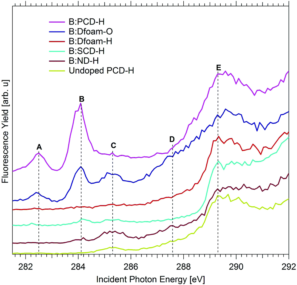 | ||
| Fig. 3 C K edge XA spectra for different morphologies of boron-doped diamond. All spectra are recorded in the PFY mode. A comparison of the spectra highlights the difference in the pre-edge features of nanostructured diamond materials such as B:Dfoam and B:ND. | ||
On B:ND-H and B:Dfoam-O, an increased intensity of peak C is also observed (Fig. 3), related to π* transition due to amorphous carbon (a-C) present at the surface and at grain boundaries of the samples respectively and also those present around sites of lattice defects induced by boron doping. Additionally, in both the samples a very broad shoulder with a threshold at 286.5 eV (D) appears very close to the conduction band minimum (CBM) just below the bulk excitonic peak E.
This shoulder is further clarified by studying the H-terminated NDs of smaller particle sizes 30 nm and 50 nm as shown in Fig. 4. Consequently, B:ND-H of smaller particle sizes 30 nm and 50 nm, both obtained by milling of commercially obtained B:PCD and subsequent centrifugation were investigated after a plasma hydrogenation treatment to remove any oxidized groups and impurities present on the surface.
 | ||
| Fig. 4 C K edge XA spectra of boron-doped hydrogenated NDs with sizes 30 nm and 50 nm. The spectra are recorded in PFY mode and compared to that of the milled NDs with average particle size below 650 nm. | ||
The two peaks A and B induced by boron doping, as seen previously in other doped samples are absent in these smaller NDs. The lower concentration of boron in these nanoparticles or surface state passivation after hydrogenation could possibly explain this observation.33 As can be seen in Fig. 4, the pre-edge region exhibits only a single peak (C) at 285.2 eV, related to π* transition from sp2 carbon, which is a direct result of high concentration of a-C at the surface and at defect sites within the NDs. The broad shoulder D is observed only in case of the nanostructured diamonds, such as B:Dfoam-O (Fig. 3) and B:ND-H (Fig. 3 and 4) with a high intensity and rather weakly in case of B:Dfoam-H. C–H bonds that result from H-terminated surface of the diamonds are expected to exhibit a π* resonance at 287.5 eV. An additional contribution from C–B bonds present on the surface could appear at 286.8 eV, as previously reported by Katamune et al.52 We consider that both these π* resonances due to C–B and C–H bonds at 286.8 eV and 287.5 eV, respectively, superpose to contribute to such a broad shoulder.
2.2 Density functional theory
Theoretical calculations have been performed to study the effect of substitutional boron doping on the formation of empty states above the valence-band edge of a diamond (111) surface. More specifically, pDOS spectra were then calculated. To evaluate the accuracy of these calculations, the calculated band gap for bulk diamond was compared with the experimental one which resulted in very similar values; 5.40 eV vs. 5.47 eV.53Three different diamond surface models were used in the study; H-terminated (111), non-terminated (111), and Pandey-chain reconstructed non-terminated (111). Fig. 1 shows the super-cells of these specific surfaces. As a p-dopant species, the element B was, with one exception, substitutionally positioned at various levels in the diamond surface models. It was either adsorbed on the surface (B-ads) or positioned in the 1st (B1), 2nd (B2) or 3rd (B3) atomic C level (see Fig. 1).
pDOS spectra of C atoms have been calculated with the purpose to investigate the boron-induced band gap states just above the valence band edge of diamond. For comparison purposes, the density of states of the non-doped surfaces have also been calculated (see Fig. 5). Since the Pandey-chain reconstructed surface is the most stable (111) surface at elevated temperatures, it is also the result for this specific surface that is interesting to compare with the experimental results. However, the results for also the non-terminated diamond (111) surface can be seen in the ESI.†
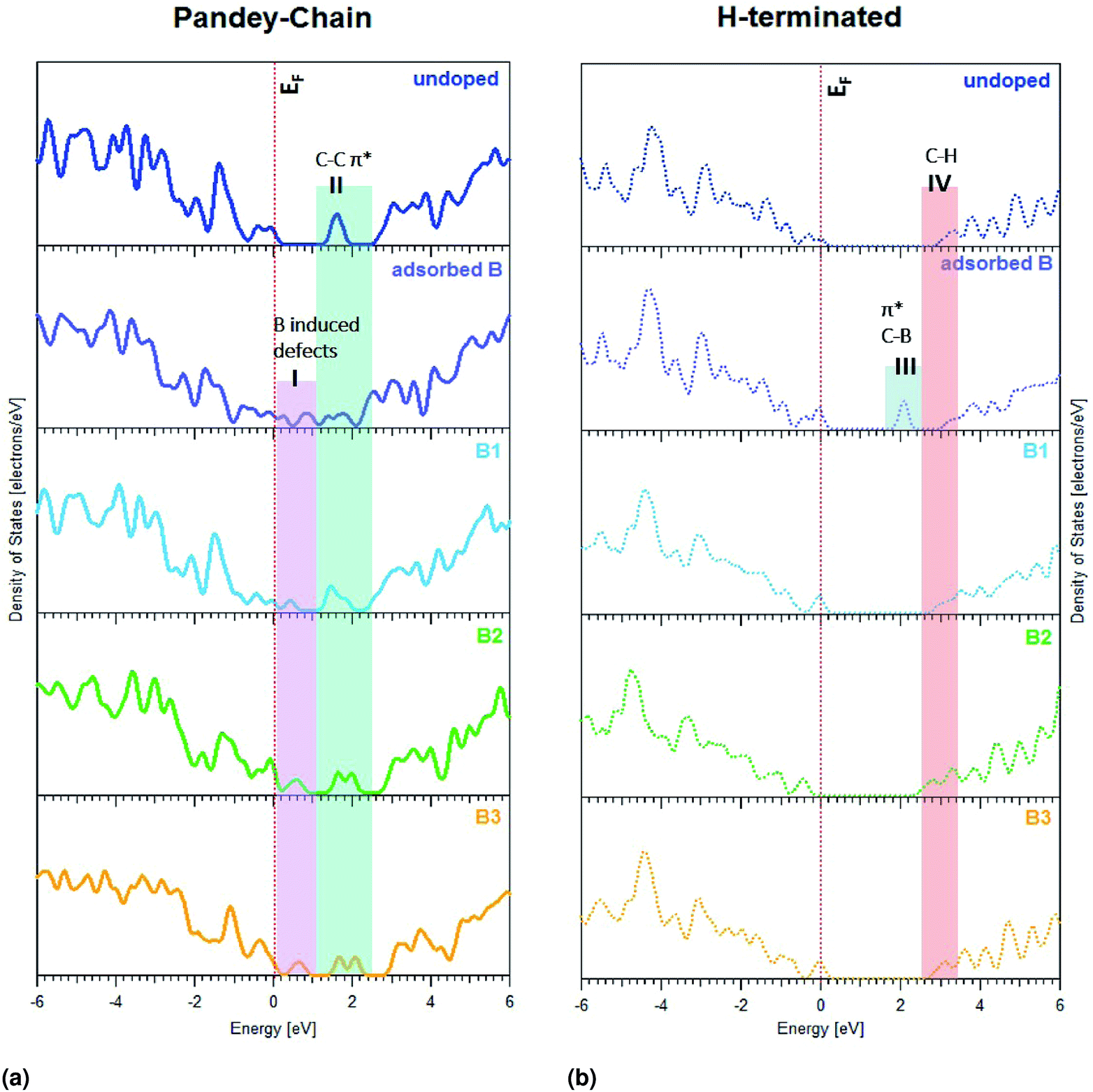 | ||
| Fig. 5 pDOS spectra of carbon at (a) Pandey-chain reconstructed and (b) H-terminated diamond surfaces. Both surfaces with boron atoms at different positions namely adsorbed B (in purple), boron in first atomic layer-B1 (in cyan), boron in second atomic layer-B2 (in green) and boron in third atomic layer-B3 (in yellow) have been compared with that of the undoped lattice (in blue). The Fermi level EF is indicated as a dotted red line at 0 eV. | ||
As can be seen in Fig. 5a and b, there are surface-induced band gap states for diamond (111) surfaces, which are much lower positioned for the non-terminated Pandey-chain reconstructed surface in comparison to the H-terminated one. The region I is induced by boron doping since it is not observed on the undoped diamond. The region II is related to π* transitions due to surface reconstruction, but are also affected by the boron doping. The lowest positioned sub band gap state for the H-terminated surface is located in region III and is not observed on the undoped sample. The states in region IV are observed for all cases and are most likely related to C–H π* transitions. The energy of this contribution varies slightly with boron doping. The pDOS spectra for the non-terminated diamond surface can be seen in ESI.†
An adsorbed boron did induce a surface state peak for the H-terminated surface at lower energy than the C–H bonds. The situation was completely different for the non-terminated and Pandey-chain reconstructed diamond surfaces. All positions of boron (i.e., adsorbed, 1st, 2nd or 3rd atomic C layer) were found to induce a surface state peak for the Pandey-chain reconstructed surface. It was only boron in layer 1 that did not render any surface peak for the non-reconstructed counterpart.
All numerical values of the boron induced mid-gap states in pDOS can be found in Table 1. More generally, it can be seen in Table 1 that boron incorporation affects the carbon atoms in the first four layers for the H-terminated and Pandey chain reconstructed diamond (111) surfaces. All C atoms sufficiently close to the B dopant will induce a surface state above the VBE for diamond 2.1 eV above the Fermi level for H-terminated surface as opposed to 0.9 eV for other surfaces. The situation is very similar for the Pandey-chain reconstructed diamond (111) surface. All C atoms sufficiently close to the B dopant will induce a surface state above the VBE for diamond. The numerical values as presented in Table 1 have been compared to experimental results in the discussion. Based on estimates from the experimental spectra, the Fermi level is placed at 283.8 eV in which case the relative positions of the sub band gap states in the boron-doped diamonds show good agreement with the theoretical estimates.
| C1a | C2a | C3a | C4a | |
|---|---|---|---|---|
| a C1, C2, C3 and C4 means that the choice of C for the pDOS calculations are within C layer 1, 2, 3 and 4, respectively. All of these specific C positions are as close as possible to the respective boron position. | ||||
| H-Terminated | ||||
| B-Ads | 2.1 | 2.1 | 2.1 | 2.1 |
| B1 | — | — | — | — |
| B2 | — | — | — | — |
| B3 | — | — | — | — |
|
||||
| Non-terminated | ||||
| B-Ads | 0.9 | 0.9 | 0.9 | 0.8 |
| B1 | — | — | — | — |
| B2 | 0.8 | 0.8 | 0.8 | 0.8 |
| B3 | 0.9 | 1.0 | 1.0 | 1.0 |
|
||||
| Pandey-chain | ||||
| B-Ads | 0.3, 0.9 | 0.2, 0.9 | 0.2, 0.9 | 0.2, 0.9 |
| B1 | 0.4 | 0.5 | 0.4 | 0.4 |
| B2 | 0.6 | 0.6 | 0.5 | 0.6 |
| B3 | 0.2 | 0.7 | 0.6 | 0.6 |
3 Discussions
Several studies have been conducted to determine the distribution of boron atoms within the diamond in order to establish a better correlation between the local environment of the boron atoms and its resulting electrical properties.54–58 While these studies clarified the distribution of boron atoms in a polycrystalline or nanocrystalline diamond film, the impact of the local interaction of boron with C atoms at or close to the diamond surface and their impact on sub-bandgap defect states of carbon in nanostructured diamond materials remain unclear. Our experimental observations show that the local environment of boron induced defects may be different within the diamond lattice for different morphologies of the doped diamonds which could modify the energy of acceptor states within the band gap of diamond materials. The possible origin of the acceptor states close to the valence band maximum (VBM) and CBM will be discussed in the following sections.3.1 Boron-induced levels close to valence band
We experimentally observe two new localized states A and B near the VBM of boron-doped diamonds, below the Fermi level of the undoped material. These states represent excitonic transitions from the C 1s core level to an empty surface state. In case of B:PCD-H and B:Dfoam-OH, the empty 2p orbitals of the boron atom hybridized with a C 2p orbital could contribute to a surface state to which a core electron from the C atom may be photoexcited. This conclusion has been supported by the theoretical calculations in the present study. All of the localized band gap states in region I of Fig. 5a coincided with pDOS peaks for boron-doped diamond. Previous microstructural investigations using HRTEM and EELS techniques on the local B environment in HPHT polycrystalline diamond films proposed that boron is present at the grain boundaries and in triangular shaped pockets at the grain junctions.54,57 However, using the same EELS technique, in case of CVD deposited boron-doped polycrystalline diamond films, Huang et al. observed no signals from B at the grain boundaries and reported that the boron atoms are uniformly distributed inside each diamond grain.55 FY intensity may vary depending on the boron concentration as previously shown by Muramatsu et al.42 In our case, the diamond materials have various boron concentrations between 300 and 6000 ppm, which could explain partly the different FY intensities between the samples. Nevertheless, surface defects are also playing a role, especially on nanostructured diamonds, as seen by the disappearance of peaks A and B after H-termination of Dfoam.All the diamond materials studied in the course of this investigation were hydrogenated at the surface. However, in case of B:PCD-H film and B:Dfoam-O, the surfaces at the grain boundaries may either contain carbon atoms with dangling bonds or C–C π-bonded dimers which may be completely or partially H-terminated thus resulting in H atoms bonded to both sp2 as well as sp3 type C atoms.59 Appearance of surface states due to dangling bonds on partially hydrogenated surfaces has already been reported by XAS investigations previously.60 Incorporation of boron in the diamond lattice occurs predominantly by substitution of a tetrahedral coordinated C atom as it results in the least amount of distortion of the diamond lattice.61 When the B atoms substitute C at the topmost layer of the lattice close to the grain boundaries, they could have two different environments. At the surfaces close to the grain boundaries, a substitutional B atom may result in C–C π-bonded dimers, resulting in surface reconstruction of diamonds, thus reducing the number of dangling bonds. Glans et al. proposed that an excitonic transition to an empty state in this case should result in a resonance similar in character to the sp2 peak C.43 However, due to extensive hybridization between the B 2p and C 2p orbitals, the core level of carbon experiences a chemical shift to lower energy resulting in the surface excitonic state to appear at a lower incident photon energy of 284.1 eV (+0.3 eV vs. EF as estimated from experiment). Theoretically, this hybridization is exhibited as a modification in the C–C π* peak in the pDOS diagram as seen in region II of Fig. 5a which is explained by an overlap between B and C orbitals. This implies that the feature B is due to surface states formed due to the sp2 C–C bonds that are in close proximity to the B atoms at reconstructed surfaces. However some carbon atoms close to the B atoms do not undergo reconstruction. Such carbon atoms have dangling bonds and are predominantly found at partially or non hydrogenated surfaces typical to grain boundaries leading to unoccupied states within the valence band.60 Glans et al. further proposed that localized states on these C atoms result in feature A.43 This furthermore validates the observation of surface excitonic states in case of the B:Dfoam-O.
The experimental observations are complemented by DFT calculations which were presented in the previous section. According to the pDOS calculations, it is quite clear that the boron atoms at the Pandey-chain reconstructed surfaces contribute to the surface states closer to the valence band edge. As B:PCD-H and B:Dfoam-O contain numerous grain boundaries,32 based on the theoretical calculations it is therefore reasonable to assert that presence of B atoms near the grain boundaries induce defects at these non-terminated surfaces resulting in the high intensity peaks attributed to surface excitonic states. However, in case of B:Dfoam-H the defect states that are predominantly present at the surface of the crystallites are completely saturated upon hydrogenation62–64 resulting in the absence of states A and B at the H-terminated surfaces as validated by theory calculations. Similar observation was reported by Barjon et al. based on cathodoluminescence measurements.63,64
Such surface excitons were also observed by Graupner et al. on clean and hydrogen terminated (111) and (100) diamond surfaces at 284.6 eV and 284.15 eV respectively.65 In case of B:SCd-H which has a (111) surface, the surface exciton peak appears very weakly at 284.1 eV. Such a red shift of 0.5 eV relative to the value reported in literature could be explained by the photoexcitation of C 1s electron from a C–C π bonded dimer into a boron 2p empty orbital, where the core level of C is also chemically shifted due to the presence of boron atoms. We can speculate that due to the absence of grain boundaries in the single crystal diamond, majority of the B atoms are present in the bulk of the crystal and hence do not induce a high concentration of defects near the surface. Since the possibility to dope a diamond (111) surface with boron is significantly higher than that of the (100) surface,66 a higher concentration of boron can be achieved in case of (111) single crystal diamonds. However, in our study B:SCd has the least dopant concentration of all the materials investigated. The substitutional boron at the surface which is lesser in concentration than that in the bulk could result in defects such as dangling bonds which are completely passivated upon H termination.63 Consequently, peak A which is attributed to dangling bond states vanishes. Reconstructions at the surface however are only weakly passivated resulting in a significantly reduced intensity of B as compared to B:PCd-H and B:Dfoam-O, in addition to the low concentration of boron in the sample.
In case of B:ND-H that is prepared by milling PC diamonds, bigger diamond crystallites are cleaved along the (111) planes.33 During ball milling, crushing of the bigger crystallites along highly defective regions is preferred. In CVD PC diamonds, which is the starting material for preparation of the boron-doped NDs, defect-rich regions have a high concentration of a-C.33 Near these defect regions, boron is usually present as substitutional tetrahedral impurities in the diamond lattice. With defects diffusing away during the crushing process,33 a significant amount of boron would also be lost resulting in a lower concentration of boron in the bulk of the resulting nanoparticles as was previously reported by Heyer et al.33 The remaining boron centers at the surface of the produced nanoparticles contribute to the weakly observed surface excitonic state B at 284.1 eV as seen in Fig. 3 which is attributed then to the surface states formed as a result of interaction between the residual sp2 C atoms and tetrahedrally substituted boron atom. The appearance of peak B with an extremely weak intensity only suggests that the defect states are partially saturated upon hydrogenation. The π* state due to the presence of sp2 C atoms on the nanoparticles further contribute towards the π* resonance C at 285.2 eV. As proposed by Turner et al., such an amorphous shell of C also surrounds the nanocrystals56 that compose diamond foams. Therefore a similar π* resonance is also observed for B-Dfoam:O.
3.2 Boron-induced levels close to conduction band
What seems to differentiate the nanostructured morphologies of boron-doped diamond from the other samples studied in this investigation is the additional broad shoulder near the conduction band edge extending from ca. 286.5–288.7 eV. This additional feature is observed with a higher intensity for B:Dfoam-O as well as B:ND-H with sizes up to 10 nm. The presence of this peak is indicative of presence of C–B bonds at the surface of the nanostructured diamonds.52 Our hypothesis here is that, in addition to the substitutional boron at the topmost layer of the diamond lattice, some of the carbon atoms at the surface with single dangling bonds bind to the B atoms which could originate from amorphous B4C type inclusions58 in nanocrystalline diamonds in order to reduce the surface energy during the doping process. Such inclusions were previously reported to be trapped in PC diamonds during their growth process.57,58 With a bond dissociation energy of ca. 448 kJ mol−1, the C–B bond once formed is much stronger than a C–H bond. Hence hydrogenation treatment of the boron doped nanostructured diamonds cannot eliminate C–B bonds that are formed at the surface. The possibility of boron coordinated to the C atoms when not embedded in the diamond lattice is further confirmed by DFT calculations. The pDOS calculations for the adsorbed boron (B-ads) configuration in case of H terminated (111) diamond surface as shown in region III of Fig. 5b evidences the appearance of a surface state closer to the conduction band, 2.1 eV above EF which is in relative agreement with the experimentally estimated value of 3.0 eV vs. EF. The presence of such a bond results in a π* resonance at 286.8 eV as was observed by Katamune et al.52 For NDs smaller than 50 nm, the absence of surface excitonic peaks in the XA spectra indicates that most of the boron is present in the form of C–B bonds at the surface of the nanoparticles and that the defects induced upon surface reconstruction are milled away leaving the nanoparticle surfaces with surface defects that may have been completely saturated during the hydrogenation treatment. The concentration of substitutional boron at the surface is too low to be detected with our instrument. In case of B:Dfoam-O, besides the π* resonance due to B adsorbed on the surface, additional contribution from C![[double bond, length as m-dash]](https://www.rsc.org/images/entities/char_e001.gif) O groups51 at the oxidized surface leads to a higher intensity of the shoulder as observed in Fig. 3.
O groups51 at the oxidized surface leads to a higher intensity of the shoulder as observed in Fig. 3.
3.3 Potential implications on photocatalysis
In view of our discussions, nanostructuration along with boron doping can be proposed as a synergetic strategy that could potentially introduce defect states that are close to both the VBM and CBM of diamonds, as exhibited in Fig. 3.As shown in Fig. 6, boron doping of diamonds result in acceptor states close to both the VBM and CBM of diamonds which is a surface dominated effect as these states are not so strongly observed for the single crystal B-doped diamond. These states are therefore further enhanced upon nanostructuration. Furthermore, H-termination introduces additional states below the CBM while saturating the acceptor states close to the VBM. A combination of these two steps produces boron-doped nanostructured diamonds with enhanced surface areas which is an essential characteristic of an efficient catalyst. Furthermore, the introduction of defect states within the band gap of nanostructured diamonds, close to both the valence and conduction bands could potentially facilitate a pathway for defect-based transitions.20–24 Energy upconversion based on related principle has been demonstrated in other materials.24 In addition, the negative electron affinity of the diamond surface should also be preserved in order to generate solvated electrons, which should be the case for investigated surfaces based on DFT calculations (see ESI†). It has to be noted that other surface treatments such as ozone treatment and amination of the surface could also lead to complementary surface states close to the conduction band of diamonds.67
 | ||
| Fig. 6 Schematic illustration depicting the two ways of introducing surface states in the band gap of undoped diamond (A). One way is nanostructuration which introduces states close to the CBM due to surface groups on nanostructured diamond surfaces (B). Another means to introduces sub band gap states is boron-doping which introduces surface states close to both the CBM and VBM (C). A synergistic effect results in a broad band of surface states close to the CBM and acceptor states close to the VBM in nanostructured B-doped diamond (D). | ||
Our results show that a synergistic effect of nanostructuration and boron doping, coupled with a high surface area offered by the nanostructured diamond materials such as foam and NDs could potentially make them promising materials for application as membranes in photoelectrocatalytic cells or catalyst nanoparticles in slurry-based photocatalytic reactors respectively.
4 Conclusions
The electronic structure of boron-doped diamond materials were investigated to engineer solutions enabling eventual defect-based visible-light absorption. Different morphologies of diamonds ranging from polycrystalline to single crystals, foams and nanodiamonds were studied using soft X-ray absorption spectroscopy supported by density functional theory to understand the influence of morphology of the doped diamond materials on the electronic structure. Our observations show that B-doping close to the surface of diamond crystallites introduces electronic states in the band gap of diamond. Surface states close to the VBM were found to be predominantly present in the CVD grown polycrystalline boron-doped diamond films and doped diamond foams. These states were deduced to originate from boron doping induced surface reconstructions and dangling bonds which are likely to be found at surfaces of the crystallites. These states may be saturated upon H-termination as observed in the case of diamond foams.Additionally, boron doping in nanostructured diamonds such as foams and nanodiamonds introduces π* states close to the conduction band of diamonds related to the C–B bond. As diamonds have previously been demonstrated as promising photocatalysts due to their electron emission capabilities, it may be suggested that boron doped nanostructured diamonds could be promising sustainable photocatalysts for CO2 reduction. This calls for further research into the investigation of visible-light absorption of B-doped nanostructured diamond through defect-based transitions.
Conflicts of interest
There are no conflicts to declare.Acknowledgements
This work was supported by European Union's Horizon 2020 Research and Innovation Programme under Grant no. 665085. TP and JR acknowledge the financial support by the Volkswagen Foundation (Freigeist Fellowship no. 89592). The authors acknowledge fruitful scientific discussions with Dr Igor Vlasov and Dr Evgeny Ekimov on early versions of the manuscript. We further acknowledge the support of the staff members at BESSY II Synchrotron Research Facility.References
- R. van de Krol and M. Grätzel, Photoelectrochemical Hydrogen Production, Springer Science and Business Media, New York, 1993 Search PubMed.
- J. Azevedo, T. Seipp, J. Burfeind, C. Sousa, A. Bentien, J. P. Araújo and A. Mendes, Nano Energy, 2016, 22, 396–405 CrossRef.
- S. N. Habisreutinger, L. Schmidt-Mende and J. K. Stolarczyk, Angew. Chem., Int. Ed., 2013, 52, 7372–7408 CrossRef PubMed.
- S. Ye, R. Wang, M.-Z. Wu and Y.-P. Yuan, Appl. Surf. Sci., 2015, 358, 15–27 CrossRef.
- H. L. Tuller, Mater. Renew. Sustain. Energ., 2017, 6, 3 CrossRef PubMed.
- B. Kumar, M. Llorente, J. Froehlich, T. Dang, A. Sathrum and C. P. Kubiak, Annu. Rev. Phys. Chem., 2012, 63, 541–569 CrossRef PubMed.
- K. P. Kuhl, T. Hatsukade, E. R. Cave, D. N. Abram, J. Kibsgaard and T. F. Jaramillo, J. Am. Chem. Soc., 2014, 136, 14107–14113 CrossRef PubMed.
- M. Ming, B. J. Trześniewski, X. Jie and W. A. Smith, Angew. Chem., 2016, 128, 9900–9904 CrossRef.
- X. Zhang, Z. Wu, X. Zhang, L. Li, Y. Li, H. Xu, X. Li, X. Yu, Z. Zhang, Y. Liang and H. Wang, Nat. Commun., 2017, 8, 14675 CrossRef PubMed.
- D. Zhu, L. Zhang, R. E. Ruther and R. J. Hamers, Nat. Mater., 2013, 12, 836–841 CrossRef PubMed.
- L. Zhang, D. Zhu, G. M. Nathanson and R. J. Hamers, Angew. Chem., Int. Ed., 2014, 53, 9746–9750 CrossRef PubMed.
- V. Yu. Dolmatov, Russ. Chem. Rev., 2001, 70, 607–626 CrossRef.
- M. Akaishi, H. Kanda and S. Yamaoka, J. Cryst. Growth, 1990, 104, 578–581 CrossRef.
- H. Sumiya and S. Satoh, Diamond Relat. Mater., 1996, 5, 1359–1365 CrossRef.
- T. Irifune, A. Kurio, S. Sakamoto, T. Inoue, H. Sumiya and K. ichi Funakoshi, Phys. Earth Planet. Inter., 2004, 143–144, 593–600 CrossRef.
- M. Kamo, Y. Sato, S. Matsumoto and N. Setaka, J. Cryst. Growth, 1983, 62, 642–644 CrossRef.
- K. Suzuki, A. Sawabe, H. Yasuda and T. Inuzuka, Appl. Phys. Lett., 1987, 50, 728–729 CrossRef.
- K. Kobashi, K. Nishimura, Y. Kawate and T. Horiuchi, Phys. Rev. B, 1988, 38, 4067–4084 CrossRef.
- S. Iijima, Y. Aikawa and K. Baba, Appl. Phys. Lett., 1990, 57, 2646–2648 CrossRef.
- D. Wang, G. Xing, M. Gao, L. Yang, J. Yang and T. Wu, J. Phys. Chem. C, 2011, 115, 22729–22735 CrossRef.
- Z. Haibo, D. Guotao, L. Yue, Y. Shikuan, X. Xiaoxia and C. Weiping, Adv. Funct. Mater., 2010, 20, 561–572 CrossRef.
- J. Wang, D. N. Tafen, J. Lewis, Z. Hong, A. Manivannan, M. Zhi, M. Li and N. Wu, J. Am. Chem. Soc., 2009, 131, 12290–12297 CrossRef PubMed.
- S. Baruah, S. S. Sinha, B. Ghosh, S. K. Pal, A. K. Raychaudhuri and J. Dutta, J. Appl. Phys., 2009, 105, 074308 CrossRef.
- M. Mahboub, P. Xia, J. Van Baren, X. Li, C. H. Lui and M. L. Tang, ACS Energy Lett., 2018, 3, 767–772 CrossRef.
- A. Deneuville, Semicond. Semimetals, 2003, 76, 183–238 Search PubMed.
- E. A. Ekimov, V. A. Sidorov, E. D. Bauer, N. N. Mel’nik, N. J. Curro, J. D. Thompson and S. M. Stishov, Nature, 2004, 428, 542–545 CrossRef PubMed.
- A. T. Collins, E. C. Lightowlers and P. J. Dean, Phys. Rev., 1969, 183, 725–730 CrossRef.
- O. A. Williams and M. Nesládek, Phys. Status Solidi A, 2006, 203, 3375–3386 CrossRef.
- M. Nesládek, D. Tromson, C. Mer, P. Bergonzo, P. Hubik and J. J. Mares, Appl. Phys. Lett., 2006, 88, 232111 CrossRef.
- W. Gajewski, P. Achatz, O. A. Williams, K. Haenen, E. Bustarret, M. Stutzmann and J. A. Garrido, Phys. Rev. B, 2009, 79, 045206 CrossRef.
- H. Kato, J. Hees, R. Hoffmann, M. Wolfer, N. Yang, S. Yamasaki and C. E. Nebel, Electrochem. Commun., 2013, 33, 88–91 CrossRef.
- F. Gao, M. T. Wolfer and C. E. Nebel, Carbon, 2014, 80, 833–840 CrossRef.
- S. Heyer, W. Janssen, S. Turner, Y.-G. Lu, W. S. Yeap, J. Verbeeck, K. Haenen and A. Krueger, ACS Nano, 2014, 8, 5757–5764 CrossRef PubMed.
- K. Nishimura, K. Das and J. T. Glass, J. Appl. Phys., 1991, 69, 3142–3148 CrossRef.
- R. Zhang, S. Lee and Y. Lam, Diamond Relat. Mater., 1996, 5, 1288–1294 CrossRef.
- P. May, W. Ludlow, M. Hannaway, P. Heard, J. Smith and K. Rosser, Diamond Relat. Mater., 2008, 17, 105–117 CrossRef.
- E. A. Ekimov, V. A. Sidorov, A. Zoteev, Y. Lebed’, J. D. Thompson, E. D. Bauer and S. M. Stishov, Phys. Status Solidi B, 2009, 246, 667–672 CrossRef.
- E. A. Ekimov, O. S. Kudryavtsev, A. A. Khomich, O. I. Lebedev, T. A. Dolenko and I. I. Vlasov, Adv. Mater., 2015, 27, 5518–5522 CrossRef PubMed.
- J. Nakamura, E. Kabasawa, N. Yamada, Y. Einaga, D. Saito, H. Isshiki, S. Yugo and R. C. C. Perera, Phys. Rev. B, 2004, 70, 245111 CrossRef.
- Y. Muramatsu, T. Takebe, A. Sawamura, J. Iihara, A. Nanba, T. Imai, J. D. Denlinger and R. C. C. Perera, X-Ray Spectrom., 2007, 36, 162–166 CrossRef.
- I. Zegkinoglou, P. L. Cook, P. S. Johnson, W. Yang, J. Guo, D. Pickup, R. González-Moreno, C. Rogero, R. E. Ruther, M. L. Rigsby, J. E. Ortega, R. J. Hamers and F. J. Himpsel, J. Phys. Chem. C, 2012, 116, 13877–13883 CrossRef.
- Y. Muramatsu and Y. Yamamoto, Diamond Relat. Mater., 2013, 39, 53–57 CrossRef.
- P.-A. Glans, T. Learmonth, K. E. Smith, S. Ferro, A. D. Battisti, M. Mattesini, R. Ahuja and J.-H. Guo, Appl. Phys. Lett., 2013, 102, 162103 CrossRef.
- Y. Song and K. Larsson, J. Phys. Chem. C, 2015, 119, 2545–2556 Search PubMed.
- S. Zhao and K. Larsson, J. Phys. Chem. C, 2014, 118, 1944–1957 CrossRef PubMed.
- Helmholtz Zentrum Berlin für Materialien und Energie, Journal of Large-Scale Research Facilities, 2016, 2, A80 CrossRef.
- J. P. Perdew, K. Burke and M. Ernzerhof, Phys. Rev. Lett., 1996, 77, 3865–3868 CrossRef PubMed.
- M. D. Segall, R. Shah, C. J. Pickard and M. C. Payne, Phys. Rev. B, 1996, 54, 16317–16320 CrossRef.
- H. J. Monkhorst and J. D. Pack, Phys. Rev. B, 1976, 13, 5188–5192 CrossRef.
- B. G. Pfrommer, M. Côté, S. G. Louie and M. L. Cohen, J. Comput. Phys., 1997, 131, 233–240 CrossRef.
- Z. Shpilman, I. Gouzman, T. Minton, L. Shen, A. Stacey, J. Orwa, S. Prawer, B. Cowie and A. Hoffman, Diamond Relat. Mater., 2014, 45, 20–27 CrossRef.
- K. Yuki, T. Satoshi, O. Shinya, S. Hiroyuki and Y. Tsuyoshi, Trans. Mater. Res. Soc. Jpn., 2015, 40, 243–246 CrossRef.
- D. Takeuchi, H. Kato, G. S. Ri, T. Yamada, P. R. Vinod, D. Hwang, C. E. Nebel, H. Okushi and S. Yamasaki, Appl. Phys. Lett., 2005, 86, 152103 CrossRef.
- N. Dubrovinskaia, R. Wirth, J. Wosnitza, T. Papageorgiou, H. F. Braun, N. Miyajima and L. Dubrovinsky, Proc. Natl. Acad. Sci. U. S. A., 2008, 105, 11619–11622 CrossRef PubMed.
- J. T. Huang, C. S. Hu, J. Hwang, H. Chang and L. J. Lee, Appl. Phys. Lett., 1995, 67, 2382–2384 CrossRef.
- S. Turner, Y.-G. Lu, S. D. Janssens, F. Da Pieve, D. Lamoen, J. Verbeeck, K. Haenen, P. Wagner and G. Van Tendeloo, Nanoscale, 2012, 4, 5960–5964 RSC.
- G. Zhang, S. Turner, E. A. Ekimov, J. Vanacken, M. Timmermans, T. Samuely, V. A. Sidorov, S. M. Stishov, Y. Lu, B. Deloof, B. Goderis, G. V. Tendeloo, J. V. de Vondel and V. V. Moshchalkov, Adv. Mater., 2014, 26, 2034–2040 CrossRef PubMed.
- Y.-G. Lu, S. Turner, E. Ekimov, J. Verbeeck and G. V. Tendeloo, Carbon, 2015, 86, 156–162 CrossRef.
- S. Michaelson, O. Ternyak, R. Akhvlediani, O. A. Williams, D. Gruen and A. Hoffman, Phys. Status Solidi A, 2007, 204, 2860–2867 CrossRef.
- K. Bobrov, G. Comtet, G. Dujardin, L. Hellner, P. Bergonzo and C. Mer, Phys. Rev. B, 2001, 63, 165421 CrossRef.
- X. Hu, Y. Dai, R. Li, H. Shen and X. He, Phys. B, 2003, 327, 39–42 CrossRef.
- C. Fernández-Lorenzo, D. Araújo, J. Martín, R. Alcántara, J. Navas, M. Villar, M. Alegre, P. Volpe, F. Omnàs and E. Bustarret, Diamond Relat. Mater., 2010, 19, 904–907 CrossRef.
- J. Barjon, N. Habka, J. Chevallier, F. Jomard, E. Chikoidze, C. Mer-Calfati, J. C. Arnault, P. Bergonzo, A. Kumar, J. Pernot and F. Omnes, Phys. Chem. Chem. Phys., 2011, 13, 11511–11516 RSC.
- J. Barjon, Phys. Status Solidi A, 2017, 214, 1700402 CrossRef.
- R. Graupner, J. Ristein, L. Ley and C. Jung, Phys. Rev. B, 1999, 60, 17023–17029 CrossRef.
- A. Boussadi, A. Tallaire, O. Brinza, M. Pinault-Thaury and J. Achard, Diamond Relat. Mater., 2017, 79, 108–111 CrossRef.
- I. Boukahil, P. S. Johnson, F. J. Himpsel, R. Qiao, J. A. Bandy and R. J. Hamers, J. Vac. Sci. Technol., A, 2017, 35, 04D102 CrossRef.
Footnotes |
| † Electronic supplementary information (ESI) available. See DOI: 10.1039/c8ta05594g |
| ‡ Present Address: Max-Planck-Institut für Mikrostrukturphysik, Weinberg 2, D-06120 Halle. |
| This journal is © The Royal Society of Chemistry 2018 |