
 Open Access Article
 This Open Access Article is licensed under a
 Creative Commons Attribution 3.0 Unported Licence
Ambient-air-stable inorganic Cs2SnI6 double perovskite thin films via aerosol-assisted chemical vapour deposition†
Jack Chun-Ren
Ke
 ab,
David J.
Lewis
c,
Alex S.
Walton
bd,
Ben F.
Spencer
c,
Paul
O'Brien
cd,
Andrew G.
Thomas
*bc and
Wendy R.
Flavell
*ab
ab,
David J.
Lewis
c,
Alex S.
Walton
bd,
Ben F.
Spencer
c,
Paul
O'Brien
cd,
Andrew G.
Thomas
*bc and
Wendy R.
Flavell
*ab
aSchool of Physics and Astronomy, The University of Manchester, Manchester M13 9PL, UK. E-mail: wendy.flavell@manchester.ac.uk
bPhoton Science Institute, The University of Manchester, Manchester M13 9PL, UK. E-mail: andrew.g.thomas@manchester.ac.uk
cSchool of Materials, The University of Manchester, Manchester M13 9PL, UK
dSchool of Chemistry, The University of Manchester, Manchester M13 9PL, UK
First published on 10th May 2018
Abstract
Air-stable caesium tin iodide double perovskite (Cs2SnI6) thin films have been fabricated via aerosol-assisted chemical vapour deposition (AACVD). We compare the properties of the double perovskite films made using AACVD with those made by the widely used spin-coating method. Films with purer crystalline phase (less CsI impurity) and far better stability in ambient air can be obtained by AACVD compared with spin coating. The AACVD-grown Cs2SnI6 films retain high phase purity for at least ∼100 days aging in air with negligible CsI impurities detected over this time, as determined by X-ray diffraction. The films exhibit an optical band gap energy (Eg) of ca. 1.3 eV and a homogeneous morphology with the expected nominal stoichiometry within error, as probed by energy-dispersive X-ray spectroscopy. Overall, the characteristics of the Cs2SnI6 films are highly process-dependent, e.g. they are influenced by the presence of hydroiodic acid (HI) in the precursor solution. Without HI addition, an iodine-deficient film with more CsI is produced, which also exhibits a larger Eg of ca. 1.6 eV. In addition to bulk properties, we utilise X-ray photoelectron spectroscopy (XPS) to scrutinise the surface characteristics in detail. We find excess Sn and I located at the surfaces. This can be attributed to the presence of SnI4 from the deposition precursor vapour. Furthermore, following aging in air, an increase in CsI impurity for the AACVD (+HI)-grown film is observed, along with a reduction in SnI4 at the surfaces. Near-ambient pressure XPS (NAP-XPS) is used to examine the surface stability of AACVD (+HI)-grown films on exposure to O2 and H2O. No enhancement in the amount of CsI impurity is observed after both H2O vapour (9 mbar) and O2 (5 mbar) exposure. Nevertheless, the concentrations of tin and iodine change after exposure, suggesting that SnI4 protects Cs2SnI6 from degradation. This passivation effect of SnI4 on Cs2SnI6 surfaces is proposed to explain the additional stability of Cs2SnI6 fabricated via AACVD.
1 Introduction
In recent years, perovskite solar cells (PSCs) have attracted tremendous attention,1–8 since the first description by Kojima et al. in 2009.9 Within a decade, this type of photovoltaic technology has undergone unprecedented advances in certificated power conversion efficiency (PCE), which has reached more than 20%.4–7 As a result, the PSCs are considered to be highly promising candidates for reduction in the cost per watt of commercial solar-energy-conversion devices. Nevertheless, there are two dominant concerns still constraining the development of PSC commercialisation: toxicity and stability. To date, all of the most efficient PSCs have been composed of lead-containing light absorbers, potentially resulting in serious human-body and environmental damage. Consequently, developing lead-free perovskite materials for use in PSCs is preferable to reduce the toxicity of photovoltaic devices. In addition, the instability/degradation of typical perovskite materials, particularly when placed in a humid environment is extremely problematic;10 upon exposure to moisture, the most widely used organolead perovskite, methylammonium lead (tri-)iodide (MAPI), degrades into lead iodide with a complete loss of the nitrogen moiety.11 Many attempts to improve the stability of halide perovskites have been investigated by a variety of approaches, including the use of alternative lead precursors,12 mixed cations,13,14 and fabrication of two-dimensional perovskites.15 Nonetheless, the stability still lags behind industrial photovoltaic standards which typically require a <10% loss in power generation after utilisation of 20 years.16 Therefore, the synthesis of stable halide perovskite films for use in photovoltaics is essential for the future development of PSCs.Among lead-free halide perovskite materials, tin-based perovskites are widely investigated as tin is a group IV metal and can be isoelectronic with lead. The first pure organo-Sn PSC was reported in 2014 with an initial PCE of approximately 6%.17 However, compared to organo-Pb PSCs, organo-Sn PSCs show not only lower PCEs but even poorer atmospheric stability (typically showing degradation within an hour).17 To stabilise Sn perovskites, it is possible to replace the unstable organic cation (e.g. methylammonium, MA) with inorganic metal ions such as caesium (Cs). However, the PCEs of CsSnI3 PSCs are typically below 4%,18–20 with a current champion PCE of 4.8% reported recently.21 The stability with respect to oxidation is poor owing to the fact that Sn2+ in CsSnI3 (or MASnI3etc.) is readily oxidised to Sn4+.20 Therefore, the Sn-deficient derivative perovskite, Cs2SnI6, has been investigated as one of the most promising Pb-free light absorbers in very recent years. This is due to the tetravalent Sn in the Cs2SnI6 structure, which cannot be further oxidised. As a result, the Cs2SnI6 double perovskite can offer far better stability under atmospheric conditions containing oxygen and water vapour.22–30
The Cs2SnI6 double perovskite which is ambipolar (i.e. it can be doped as n-type or p-type) exhibits excellent carrier mobility when doped as an n-type semiconducting material. In addition, it has a relatively low optimised energy band gap (Eg) of ca. 1.3 eV and high absorption coefficient (of over 105 cm−1 for energies above 1.7 eV), which shows great potential for use as a light absorber in photovoltaic devices.22–24 Very recently, using a special architecture, Cs2SnI6-based solar cells with PCEs of ca. 2.0% and acceptable stability in air have been reported.23 By doping Br into the structure, a higher PCE of ca. 5.2% has been reported for Cs2SnBrxI6−x (x = ∼2).31 Nevertheless, many discrepancies in the properties of Cs2SnI6 have arisen, such as variations in Eg between 1.3 eV and 1.6 eV and carrier mobility (varying over the range 1–310 cm2 V−1 s−1), which are both found to be highly process-dependent.22–25 Lee et al. demonstrated that different CsI-impurity levels lead to variations in the band gap energies, carrier concentrations and mobilities, which can be controlled by preparation methods.23 Given the improvement in Pb-based perovskites, one may envisage the potential to obtain high quality Cs2SnI6 thin films with favourable characteristics for use in photovoltaics using novel preparation approaches.
Aerosol-assisted chemical vapour deposition (AACVD) is a promising process for fabrication of perovskite thin films (one-step32–34 and two-step processes35,36), since it merges the advantages from solution-based methods (low cost) and chemical vapour deposition (high quality, controlled thickness).37–40 Nonetheless, until now, AACVD studies of halide perovskites are still limited since Lewis et al. first introduced AACVD-grown organo-Pb perovskite thin films.32–35 A detailed study of AACVD-grown Sn-based perovskites, which includes characterisation of their bulk and surface properties and surface stability/degradation has not been reported thus far. In this work, we utilise a one-step AACVD process to fabricate high quality Cs2SnI6 thin films for the first time. A thorough study of the fabrication and characterisation of Cs2SnI6 material is also provided. By applying this facile, scalable process, films with high purity and uniformity can be obtained. The growth of films at a relatively low temperature of 150 °C is well adapted to flexible device applications,41–45 when compared to vacuum deposition (190 °C).25 We also demonstrate the importance of addition of hydroiodic (HI) acid to the precursor solution to afford Cs2SnI6 films with a reduced number of macroscopic defects such as pinholes. Iodine vacancies (VI) are easily formed as well as tin interstitials (Sni) in this material.29 HI is selected for two reasons: firstly, it is an ideal iodine source to afford I-rich Cs2SnI6 material. Secondly, using excess SnI4 to supply iodine could potentially lead to deleterious formation of Sni. We also employ near-ambient pressure X-ray photoelectron spectroscopy (NAP-XPS) to measure the in situ degradation of the AACVD-grown films prepared with the addition of HI. By combining XPS data from a number of experiments, we show that surface passivation through a layer containing excess Sn and I is one factor imparting stability of the Cs2SnI6 films. These insights will help the future development to Pb-free halide perovskites for use in photovoltaic devices.
2 Experimental
2.1 Sample preparation
Firstly, 0.5196 g of caesium iodide (CsI, 99.9%, Aldrich) was added into 10 mL of warm (∼70 °C) anhydrous N,N-dimethylformamide (DMF, 99.8%, Sigma-Aldrich) solvent with gentle stirring to generate a clear pale-yellow solution (0.2 M). A stoichiometric amount (0.6263 g, 0.1 M) of tin(IV) iodide (SnI4, 99.999%, Aldrich) was poured into the solution. The colour of the precursor solution immediately became dark brown and then black after a few minutes. A small amount (300 μL, 0.2 M) of hydroiodic acid (HI, 57 wt%, Aldrich) was added to produce an I-rich solution (denoted as +HI). Another precursor solution was prepared without the addition of HI (denoted as −HI) for comparison. The resulting solutions were used for the AACVD process or spin-coating.The prepared solution was directly used as the feed for AACVD without further procedures. The apparatus used for AACVD has been previously described in detail by Ramasamy et al.46 Firstly, 10 mL of the DMF solution was poured into a two-necked 100 mL round-bottom flask with a gas inlet. This allows Ar carrier gas (flow rate ∼300 sccm) to pass into the solution to support the transport of aerosol generated by a humidifier. This flask was connected to a tube in a furnace where the temperature during deposition was set to 130 °C. Indium tin oxide (ITO)-coated glass (Ossila) with a size of 2.0 × 1.5 cm or gold-coated silicon (Au–Si) were utilised as substrates. The deposition rate was approximately 20 nm per minute as measured by a Veeco Dektak 8 Surface Profilometer and the deposition time was set for an hour. As a result, we obtained films with a thickness of around 1.2 μm on the substrates. Following the deposition, the samples were annealed at 150 °C in ambient air to remove residual solvent from the samples and tube for 30 minutes. The sample was then allowed to cool to below 100 °C before removal from the AACVD tube. The prepared samples were placed into (sample) tubes filled with Ar and then stored in a small desiccator. For the aging study, the films were aged in ambient air at an average relative humidity (RH) of >70% for periods up to ∼100 days. All fresh samples were exposed to ambient air for less than 10 minutes when transferring from the growth tubes to a characterisation chamber.
A small volume (100 μL) of the same precursor solutions (+HI) was also used to prepare spin-coated films of similar (∼1.2 μm) thickness for comparison. The films were deposited at 4000 rpm for 30 seconds and subsequently transferred to a hot plate for annealing at 150 °C in air for 30 minutes. The resultant samples were stored or aged in the same way as the AACVD-processed samples.
2.2 Instrumentation
X-ray diffraction (XRD) patterns were recorded using a Bruker D8 Advance. A grazing incidence (GI) angle of 3° was used to detect the signals from the thin films without the substrates. The scanning range (2θ) was recorded from 5° to 80° with a step size of 0.05° and dwell time of 4.5 s.The morphology of the films was measured using scanning electron microscopy (SEM) and bulk elemental analysis was carried out using an energy-dispersive X-ray spectroscopy (EDX, Philips XL30 equipped with a DX4 EDX spectrometer). EDX was conducted in the SEM chamber and the error in bulk stoichiometry measurements was ±2%.
Optical diffuse reflectance measurements were performed using an ultra-violet-visible-near-infra-red (UV-VIS-NIR) spectrometer (PerkinElmer Lambda-1050) with an integrated sphere (IS) module to collect the scattered light. Spectra were recorded over a wavelength range of 300 to 1500 nm from samples deposited on soda-lime glass substrates. Reflectance (R) was automatically converted to absorption (α) data in accordance with the Kubelka–Munk equation. The optical energy band gap (Eg) was acquired using a Tauc plot to find the onset point of the absorption spectra.
X-ray photoelectron spectroscopy (XPS) measurements were performed with either a Kratos Axis Ultra or SPECS XPS instrument. Both facilities are equipped with monochromated Al Kα X-ray sources with a photon energy of 1486.6 eV. Emitted photoelectrons were collected using either a 165 mm hemispherical energy analyser (Kratos) or a 150 mm hemispherical energy analyser (Phoibos 150 SPECS), respectively. All measurements conducted in this section were carried out in ultra-high vacuum (UHV) conditions. Binding energies (BEs) were calibrated to C 1s from adventitious carbon at 284.8 eV for ITO-glass substrates or Au 4f7/2 at 84.0 eV for Au–Si substrates.
The SPECS instrument also allows for NAP-XPS measurements to be carried out and the details can be found elsewhere.11 The NAP cell is equipped with differential pumping to enable gas pressures up to ∼15 mbar to be applied during measurement. In this work, 9 mbar water vapour (RH = ∼30%) and 5 mbar oxygen were separately applied. All XPS data were analysed using CasaXPS software, in which a Shirley background and pseudo-Voigt peaks (30% Lorentzian and 70% Gaussian) were fitted to the photoelectron peaks acquired.47
BE values are quoted to an accuracy of ±0.1 and ±0.05 eV for typical and in situ XPS study, respectively, due to instrumental precision. To obtain quantified surface compositional information, the built-in CasaXPS sensitivity factors (Kratos, relative to F 1s as 1.0) are utilised for calculating the available stoichiometry. Note that this does not allow the quantitative analysis of spectra acquired at near-ambient pressure (NAP) conditions due to the absence of adapted transmission-function data. All surface elemental concentrations are normalised to Cs (Cs 3d5/2 spectra) as 2 in an ideal stoichiometric Cs2SnI6 film. Excess concentrations of Sn and I above 1 and 6, respectively are likely to indicate the presence of non-Cs2SnI6 species.
3 Results and discussion
Following annealing under ambient air in the AACVD reactor, highly uniform and black AACVD (+HI)-processed Cs2SnI6 films were formed, as shown in Fig. 1A. This indicates strong visible-light absorption by the as-prepared AACVD (+HI)-grown Cs2SnI6 film as the part of the logo covered by the film is barely visible. Following ∼100 days storage under ambient air (average RH > 70%), the appearance of the film (Fig. 1B) is similar to the fresh sample (Fig. 1A). This suggests that there is no significant change in the visible light absorption of the film after being aged in a humid environment. Peeling and scratching tests suggest that the AACVD films produced here show significantly better adhesion to the substrates than the spin-coated films prepared under similar conditions (see ESI, Fig. S1†).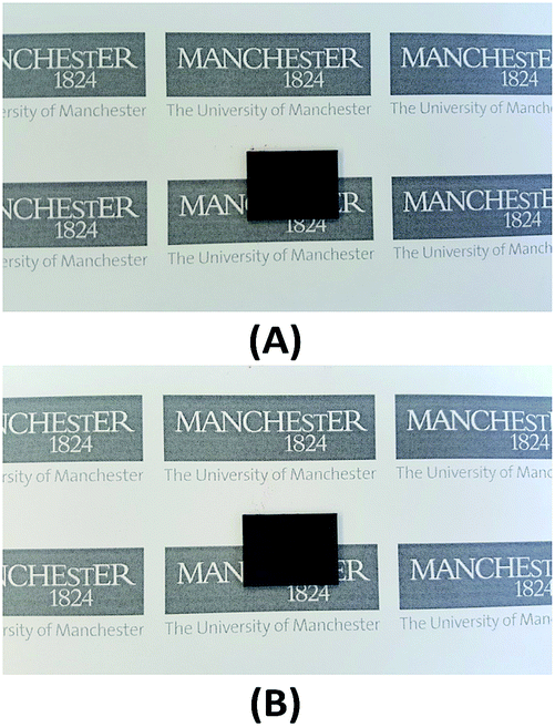 | ||
| Fig. 1 Photographs of an AACVD (+HI)-grown Cs2SnI6 film on ITO-glass substrates: (A) as-deposited (B) after aging in ambient air for ∼100 days. The thicknesses of the films are around 1.2 μm. | ||
In order to determine the crystalline phase, grazing incidence X-ray diffraction (GIXRD) patterns of various films (Fig. 2) were examined. Fig. 2A shows XRD reflections of a typical AACVD (+HI)-grown film as a function of aging time (up to ∼100 days). For the pristine sample, the XRD peaks indicate that the crystal structure is in excellent agreement with the Cs2SnI6 double perovskite structure (JCPDS no. 51-0466, cubic, space group Fm3m, a = 11.65 Å).26 The dominant (strongest) diffraction peak from the (222) crystal plane at 26.55° and other primary peaks such as (400) are also annotated in the figure. The face-centred-cubic double perovskite structure (with Sn deficiency at the centre) increases the intensity of the (222) reflection relative to the (111) reflection.22 A more detailed examination reveals a diffraction peak due to the (110) reflection from a trace amount of the cubic CsI impurity at 27.60° (JCPDS no. 89-4257).48 The amount of this contaminant is very low in fresh samples (Fig. 2A), suggesting that the AACVD process allows formation of highly pure Cs2SnI6 crystalline films. In addition, we observe that the AACVD (+HI)-processed film appears to be highly stable following ∼10 and ∼100 days exposure to air (Fig. 2A). The amount of CsI impurity remains low and there are no other new crystalline phases generated. The ratios of the intensity of the CsI (110) reflection to that of the Cs2SnI6 (220) reflection are summarised in Table 1. This highlights the relatively small change in the amount of CsI impurity when aged in ambient air. As shown, the ratio is in the vicinity of ∼0.020 after 100 days' aging, showing that AACVD (+HI)-processed Cs2SnI6 is significantly more stable than the widely used methylammonium lead iodide perovskite. MAPI is easily transformed to lead iodide (PbI2) under ambient air within a week due to reaction with moisture in the environment.49
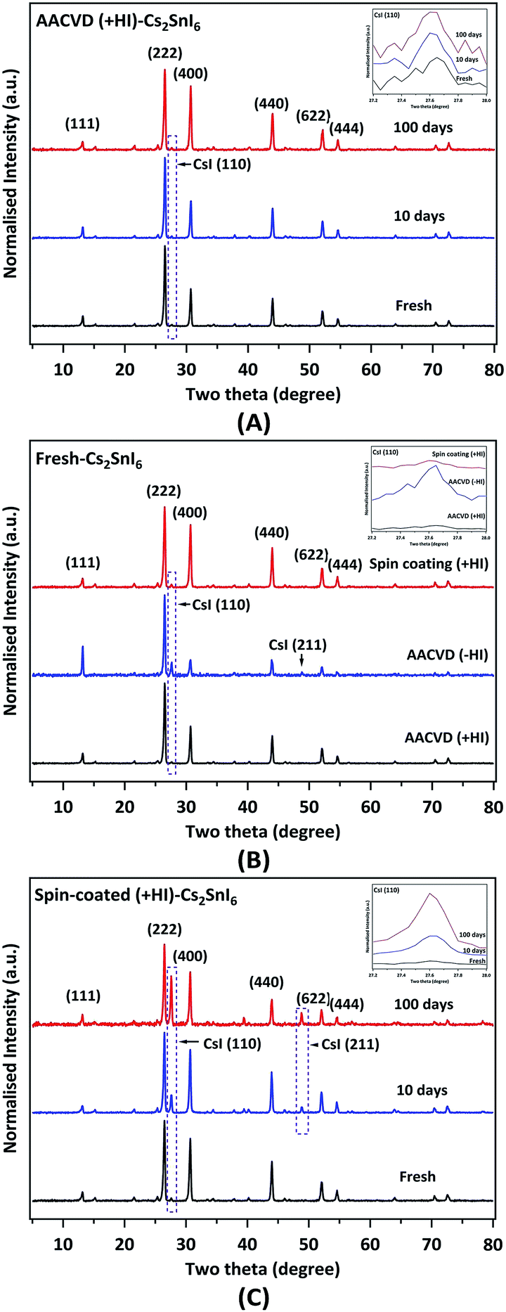 | ||
| Fig. 2 XRD patterns of Cs2SnI6 films on ITO-glass substrates recorded with a grazing incidence (GI) angle of 3° showing: (A) the effect of aging in air (RH > 70%) on AACVD (+HI)-processed film, (B) samples obtained from different precursor solutions and deposition processes (as annotated), and (C) the effect of aging on a spin-coated sample. The primary peaks for both Cs2SnI6 and CsI are indicated; the purple dashed squares highlight the 2θ range for the dominant (strongest) reflection of the CsI impurity. The top-right inset in each figure shows the expansion of the CsI (110) region. | ||
| Sample ID | I CsI(110)/ICs2SnI6(222) (XRD) | Cs/Sn (EDX) | I/Sn (EDX) | E g | CsI/Cs2SnI6 (XPS) |
|---|---|---|---|---|---|
| AACVD (+HI) fresh | 0.016 ± 0.002 | 2.0 ± 0.1 | 6.0 ± 0.2 | 1.30 | 0.14 ± 0.01 |
| AACVD (+HI) 10 days | 0.021 ± 0.002 | 2.0 ± 0.1 | 5.9 ± 0.2 | — | — |
| AACVD (+HI) 100 days | 0.024 ± 0.002 | 2.0 ± 0.1 | 5.8 ± 0.2 | 1.35 | 0.20 ± 0.02 |
| AACVD (−HI) fresh | 0.160 ± 0.020 | 1.9 ± 0.1 | 5.6 ± 0.2 | 1.60 | 0.34 ± 0.03 |
| Spin-coated (+HI) fresh | 0.034 ± 0.003 | 2.0 ± 0.1 | 5.8 ± 0.2 | 1.35 | 0.21 ± 0.02 |
| Spin-coated (+HI) 10 days | 0.218 ± 0.020 | 1.9 ± 0.1 | 5.4 ± 0.2 | — | 0.35 ± 0.04 |
| Spin-coated (+HI) 100 days | 0.600 ± 0.060 | 1.9 ± 0.1 | 4.9 ± 0.2 | 1.60 | — |
Fig. 2B shows the effect on crystal structure produced by the addition of HI in the precursor solution. In the absence of HI, a noticeable amount of CsI impurity is present (ICsI(110)/ICs2SnI6(222) = ∼0.160, 10 times more than that observed in the AACVD (+HI)-grown films, as shown in Table 1). This indicates that the synthesis process (+HI or −HI) can significantly influence the crystalline phase composition. In the relatively I-poor environment (−HI), iodine vacancies (VI) can form more easily.29 A density functional theory (DFT) study suggests VI and interstitial tin (Sni) are the dominant defect types in Cs2SnI6.29 The optimised molar concentration of HI in the precursor solution to minimise the CsI impurity phase was found to be 0.2 M, as described in the Experimental section. The concentration is roughly equivalent to twice the SnI4 precursor molar concentration, in good agreement with the following reaction for formation of [SnI6]2− octahedra in Cs2SnI6:50
| SnI4 + 2I− → [SnI6]2− | (1) |
Thus it appears that excess iodine (in an I-rich environment) facilitates the formation of the [SnI6]2− sub-lattice of the Cs2SnI6 double perovskite material. Not only do the different preparation methods lead to distinct phase compositions but the stability can also be affected by the thin film deposition method. The preparation route used to synthesise Cs2SnI6 has been shown to be a critical factor governing its stability.25 Samples prepared by spin coating were found to contain a significant CsI impurity phase after only 5 days under ambient air.22,25Fig. 2C shows the effect of aging in ambient air on samples prepared by spin coating. There is a significant increase in CsI content with aging compared to the AACVD (+HI)-processed sample. The ICsI(110)/ICs2SnI6(222) ratio of the pristine spin-coated (+HI) film is attributed to a slightly higher initial impurity level (∼0.034) relative to that of the pristine AACVD (+HI)-grown film. After 100 days, a substantial amount (∼0.600) of CsI is observed in the spin-coated film. As described, the precursor solution (+HI) and the annealing process are identical between the AACVD and spin-coating processes. Therefore, the difference in stability can be attributed to the method used to prepare the thin films. The amount of CsI appearing with time in the AACVD (+HI)-processed samples is compared with the results of Saparov et al. for films deposited by vacuum deposition in Fig. S2 (ESI†).25 This suggests that the stability of the Cs2SnI6 films fabricated by AACVD is comparable to or even better than that of films made via vacuum vapour deposition.25 We note that the AACVD (+HI)-grown films were placed in an ambient environment with higher relative humidity (R.H. > 70%) when compared to the environment in the work of Saparov and others.25 These results suggest that AACVD (+HI) can produce Cs2SnI6 double perovskite films that are stable in humid air.
Nevertheless, films prepared by both AACVD and spin-coating were degraded (to a lesser or greater extent) producing CsI when aged in ambient air. This may imply a bulk decomposition mechanism:
| Cs2SnI6 → 2CsI + SnI4. | (2) |
Clearly, to generate CsI by decomposition of Cs2SnI6, SnI4 should be formed in accordance with this reaction. However, no peaks which can be assigned to SnI4 are observed in the XRD patterns. This may be because SnI4 is somehow absent, which we discuss in later sections. In order to determine whether the film quality could be influencing the stability of the films, the morphology of the as-prepared films was examined using SEM, as shown in Fig. 3. The crystal structures at high magnification for samples produced by AACVD (+HI), AACVD (−HI), and spin-coating (+HI) are shown in Fig. 3A, C, and E, respectively. All of the samples show micrometre-sized octahedral grains; however, the average size of the grains is larger for the AACVD (+HI)-Cs2SnI6 film. The shape of the crystals in films made without HI is less well-defined, with what appears to be melted material at the surface.
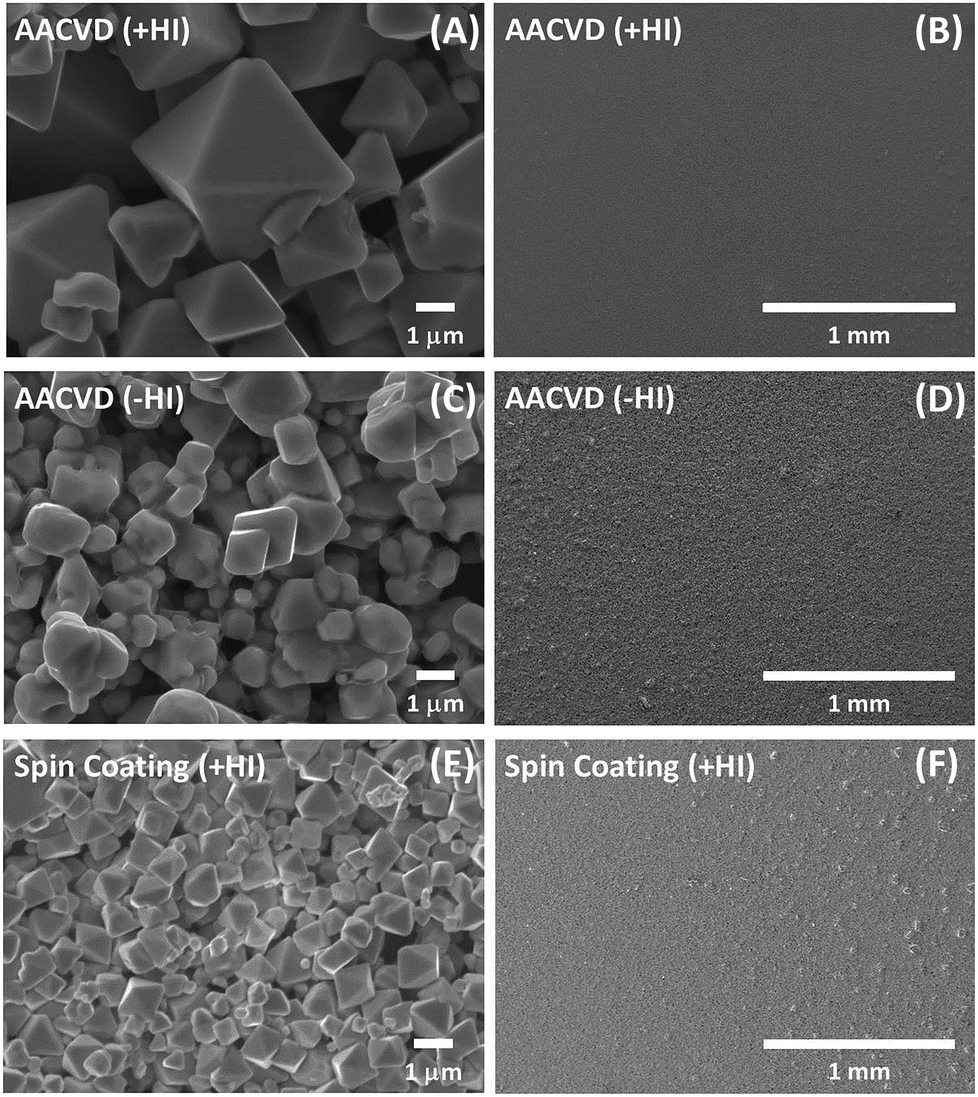 | ||
| Fig. 3 SEM images of fresh Cs2SnI6 films on ITO-glass substrates (A & B) AACVD (+HI)-processed film, (C & D) AACVD (−HI)-grown film, and (E & F) spin-coated (+HI) film at higher (A, C & E) and lower (B, D & F) magnifications. | ||
SEM shows that the different processing techniques lead to differences in grain sizes. Larger grain sizes for the AACVD (+HI)-Cs2SnI6 film have a lower overall surface-to-volume ratio, and are thus more resilient to atmospheric degradation partially contributing to an enhanced stability. By measuring grain sizes for the different films, we estimate that the surface area of the AACVD (+HI)-grown film (Fig. 3A) is approximately 16× that of the film prepared by spin coating (Fig. 3E). However, the rate of degradation of the spin-coated film is ca. 70× that of the AACVD (+HI)-prepared film, as estimated from XRD (Fig. S2†). This suggests that additional factors are important in determining the stability of the AACVD-prepared films.
At a lower magnification, the homogeneity of the films is shown in Fig. 3B, D, and F. The AACVD (+HI)-processed film (Fig. 3B) is very smooth, uniform, and (relatively) pin-hole free, which is important to its application as a light absorber in photovoltaic devices.51 The other two samples (Fig. 3D and F, AACVD (−HI) and spin-coated (+HI) respectively) show higher roughness, less homogeneity, and more pinholes. This could also contribute to differences in the stability between AACVD and spin-coated samples. Degradation sources such as water vapour or oxygen are able to enter the bulk via pinholes or pores more easily. This is consistent with the rapid and more obvious degradation of the spin-coated film as measured by XRD compared to the AACVD-grown films.
The bulk stoichiometries of the films, as determined by energy-dispersive X-ray (EDX) spectroscopy, are also shown in Table 1. The AACVD (+HI)-prepared sample has the expected elemental stoichiometry of ideal Cs2SnI6 within experimental error. The Cs![[thin space (1/6-em)]](https://www.rsc.org/images/entities/char_2009.gif) :Sn ratios for all samples are very similar, and lie in the range 1.9–2.0. This suggests that if Cs2SnI6 is converted into CsI, the CsI impurity and Sn degradation products remain in the film since it is unlikely that both are lost at the same rate. Nevertheless, the ratios of iodine to tin do show some variations, indicating a clear loss of iodine with aging for the spin-coated sample. Moreover, the slight lack of iodine in the fresh AACVD (−HI)-grown sample indicates that in an I-poor environment, VI defects tend to be generated.
:Sn ratios for all samples are very similar, and lie in the range 1.9–2.0. This suggests that if Cs2SnI6 is converted into CsI, the CsI impurity and Sn degradation products remain in the film since it is unlikely that both are lost at the same rate. Nevertheless, the ratios of iodine to tin do show some variations, indicating a clear loss of iodine with aging for the spin-coated sample. Moreover, the slight lack of iodine in the fresh AACVD (−HI)-grown sample indicates that in an I-poor environment, VI defects tend to be generated.
The optical band gap energies (Eg) of the films were determined using ultraviolet-visible-near-infrared (UV-VIS-NIR) spectroscopy. The Tauc plots (Fig. 4) were obtained from the absorption spectra transformed from the diffuse reflection spectra via the Kubelka–Munk function. Cs2SnI6 is typically referred to as a direct bandgap material, which has been confirmed by photo-luminescence results.22,23,52 By determining the onset of the plots, the value of Eg was obtained for the different samples. In Fig. 4A, we observe that the AACVD (+HI)-grown Cs2SnI6 film has a bandgap of ca. 1.30 eV, which is consistent with the smallest value in the range previously reported (1.3–1.6 eV).22–25,52,53 Following aging for ∼100 days, the band gap energy increases slightly to ca. 1.35 eV. More significant differences are observed in comparing films prepared with and without the addition of HI. Fig. 4B shows that the AACVD (−HI)-prepared sample has a relatively high Eg of ca. 1.60 eV. This again suggests that iodine deficiency or the presence of CsI impurities can significantly influence the properties of the Cs2SnI6 thin films. It can be observed in Table 1 that an increase in CsI impurity level leads to higher Eg, in good agreement with a recent finding.23 Lee et al. found that, by using spin-coating with different parameters, varying levels of CsI impurity were formed in Cs2SnI6 films.23 This results in a range of Eg values from 1.3 to 1.4 eV as well as differences in carrier concentration and mobility.23 Our study further demonstrates that the characteristics of Cs2SnI6 films are highly process and defect dependent. Therefore, innovation in the preparation of Cs2SnI6 films is of importance in optimising these characteristics.
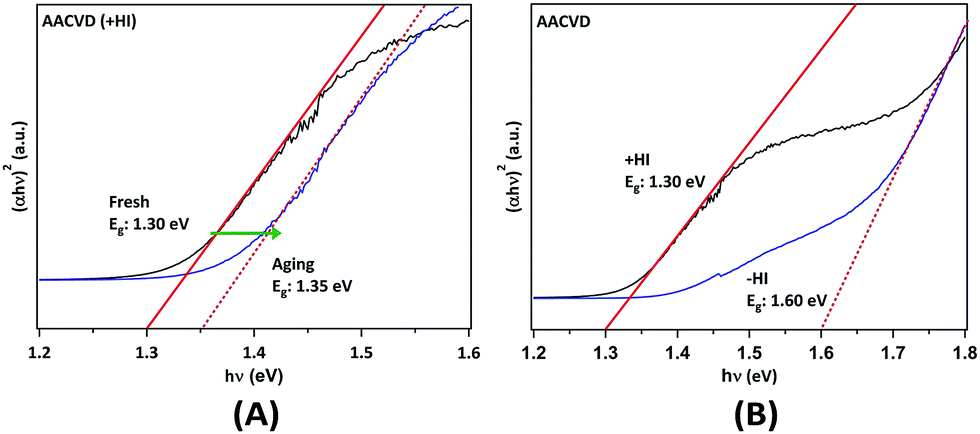 | ||
| Fig. 4 Tauc plots from the UV-VIS-NIR spectra of AACVD-grown Cs2SnI6 thin films obtained via the Kubelka–Munk equation by taking Cs2SnI6 as a direct band gap semiconductor: (A) the fresh and aged AACVD-prepared film and (B) with (+HI) and without (−HI) HI addition in the precursor solutions. | ||
These results illustrate the effects of degradation and the intrinsic differences between the bulk properties of the films prepared by various methods. The surface characteristics are equally important since degradation occurs at the solid–vapour interfaces first, where the surfaces are in contact with degradation-inducing reactants. The X-ray photoelectron spectra (XPS) shown in Fig. 5 depict the surface compositions of various fresh and aged films obtained by recording the Cs 3d core levels. Two components, giving rise to two 3d5/2,3/2 doublets, are observed for all of the double perovskite samples, both fresh and aged. The higher and lower binding energy (BE) Cs 3d5/2 components, located at 725.1 ± 0.1 eV and 724.2 ± 0.1 eV, can be attributed to CsI and Cs2SnI6, respectively.54 The assignment of the CsI features is also confirmed by comparison with spectra of a spin-coated pristine CsI film, also shown in Fig. 5. Moreover, we observed that each sample showed different surface CsI-impurity levels; spectra of films with a significant amount of CsI show pronounced high-binding-energy shoulders in the Cs 3d peaks (3d5/2 and 3d3/2). In order to easily compare, the area ratios of the CsI to Cs2SnI6 Cs 3d5/2 components fitted are summarised in Table 1. The amount of CsI surface impurity in the AACVD (+HI)-prepared sample increases only slightly after aging for ∼100 days (CsI:Cs2SnI6 increases from 0.14 ± 0.01 to 0.20 ± 0.02). By contrast, that of the spin-coated film significantly increases (corresponding ratios 0.21 ± 0.02 to 0.35 ± 0.04) as a result of aging for a much shorter period (10 days).
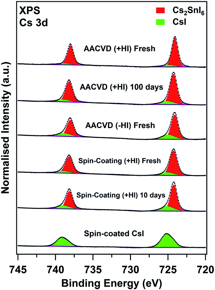 | ||
| Fig. 5 XPS spectra of the Cs 3d region for various Cs2SnI6 samples and a spin-coated CsI film for reference. All spectra are normalised to the integrated area of the overall Cs 3d5/2 peaks (Cs2SnI6 + CsI). | ||
This indicates the surface stability of the AACVD (+HI)-grown film is better than the spin-coated one, and this is consistent with the findings from the bulk properties. Interestingly, we observe that the CsI:Cs2SnI6 ratio in the fresh sample fabricated without HI (0.34 ± 0.03) is similar to that of the aged spin-coated sample. These observations suggest that the presence of CsI impurity at the surfaces is strongly influenced by the preparation process. Table 1 shows that the variations between films in the relative amount of CsI impurity found at the surface are similar to the trends observed in the bulk. While we cannot directly compare the concentrations determined from XPS with the ratio ICsI(110)/ICs2SnI6(222) obtained from XRD, we note that for the AACVD (+HI)-grown films, the surface CsI:Cs2SnI6 ratio is approximately ten times that of ICsI(110)/ICs2SnI6(222), whereas for the more degraded films this factor is lower (approximately 2–5). This suggests that in the initial stages of degradation, CsI is localised at the film surfaces.
In addition to the amounts of CsI impurity, the stoichiometry of the other elements is of importance in understanding the surface compositions of the various films, and is shown in Table S1.† In order to easily observe deviations from stoichiometry at the surface of the films, we normalise the calculated ratios of the elements to [Cs] = 2.0 (i.e. Cs2SnxIy), as for an ideal stoichiometric Cs2SnI6 film. We found that all samples, whether fresh or aged, and regardless of preparation method contain excess Sn ([Sn] > 1). These Sn atoms could originate from the SnI4 precursor as we also observe excess I at the surface in all samples. For the fresh AACVD (+HI)-grown sample, the excess I is close to 4 times the excess Sn. This suggests the presence of SnI4 in significant excess, as the excess values for I and Sn are high. In addition, the amount of SnI4 is far more than that of CsI, suggesting that the majority of the SnI4 does not originate from the decomposition process in eqn (2). As fresh AACVD-grown films have a larger excess of I and Sn, we speculate that the residual SnI4 vapour in the AACVD tube attaches to the outermost surfaces of the film. This may occur particularly during the cooling process at temperatures of ∼100-150 °C, when the reaction between SnI4 and CsI cannot happen. The more volatile component, SnI4,50 continues to be transported along the tube and condenses on the surface of the film during the cooling cycle. The relative changes in Sn concentration can also be observed in Fig. S3† by comparing the intensities of the Cs 3d5/2 and Sn 3p3/2 peaks.
After aging the AACVD-grown film in ambient air, the excess Sn decreases somewhat while the concentration of excess I is very significantly reduced. This suggests the SnI4 at the surfaces undergoes decomposition (loss of iodine) with I2 or HI release from the film by some mechanism. SnI4 is known to be easily hydrolysed in the presence of water, so the SnI4 at the surfaces is expected to react with moisture, forming hydrated SnO2 (SnO2·nH2O).55–58 By comparison, the changes in the surface composition of the spin-coated film on aging are much smaller, starting from a smaller initial excess of Sn and I. This reinforces the suggestion that the excess SnI4 on the surfaces of the AACVD-prepared samples is due to the nature of the process. Interestingly, the fresh AACVD (−HI)-grown sample contains a very significant amount of excess Sn but a lower excess of I compared to the fresh AACVD (+HI)-prepared film, consistent with the EDX finding. The large excess of Sn could be due to a significant amount of I-deficient tin iodide, and I-deficient Sn sites within the perovskite phase. This also suggests again that without addition of HI, the formation of Cs2SnI6 cannot be facilitated as per eqn (1).
It is clear that changes in surface composition of the films are observed after aging in air even for the relatively stable AACVD (+HI)-grown sample. It is therefore of interest to identify which gases in air (e.g. H2O vapour or O2) are responsible for the surface degradation. NAP-XPS is a novel technique which allows investigation of the surface stability and degradation mechanisms of halide perovskite materials.11 This is because this technique enables the surface composition of the films to be measured under near-ambient pressure (NAP) conditions in a chamber filled with specific gases, and changes during gas exposure can be determined. In this study, the effects of water vapour and oxygen were explored. The Cs 3d NAP-XPS spectra recorded from fresh AACVD (+HI)-grown Cs2SnI6 films during and after exposure to O2 (5 mbar) and water vapour (9 mbar, corresponding to ∼30% RH at 25 °C) are shown in Fig. 6. The two samples were prepared from the same initial sample by cutting it into two pieces. Following water vapour exposure (Fig. 6A), we observe that the CsI component does not increase relative to Cs2SnI6. Similarly, no obvious change was found in the Cs 3d spectra before and after the film was exposed to O2. These results suggest under those environments, the films do not degrade significantly via the mechanism in eqn (2), which should form CsI and SnI4.
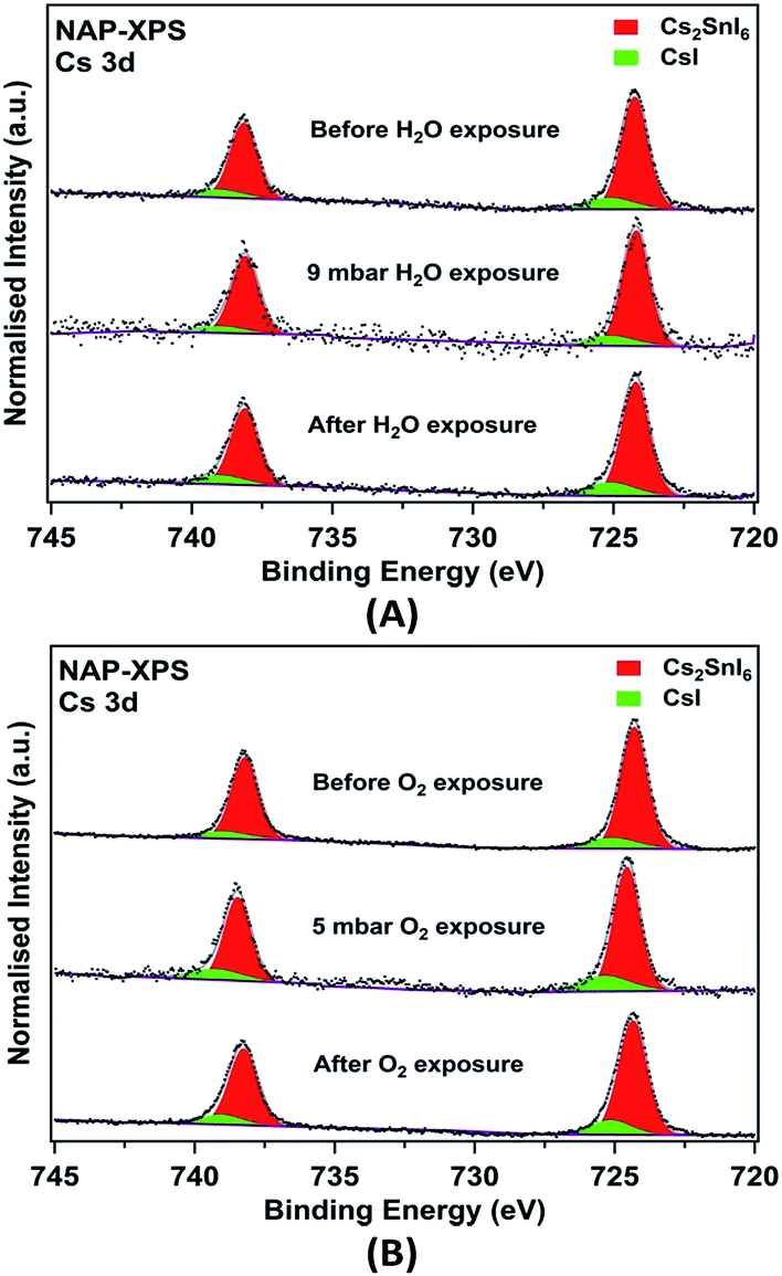 | ||
| Fig. 6 NAP-XPS Cs 3d core-level spectra of AACVD (+HI)-grown films before, during, and after exposure to (A) 9 mbar H2O vapour and (B) 5 mbar O2. All spectra are normalised to the Cs 3d5/2 peak areas for comparison. | ||
This is possibly as a result of insufficient exposure time as well as the limited gas pressure in the chamber. However, as compared to similar studies of MAPI, it is clear that Cs2SnI6 shows higher resistance to moisture when both films are exposed to environments with a RH of ∼30%.11 Cs remains at the surfaces of the Cs2SnI6 film, whereas the equivalent ‘A’ cation in the ABX3 perovskite structure of MAPI, the methylammonium ion (CH3NH3+), decomposes and nitrogen is lost from the surfaces of the film in the form of ammonia gas. Other core level spectra (I 3d, Sn 3d, C 1s, and O 1s) recorded from the films are shown in Fig. S4† for H2O vapour and Fig. S5† for O2 exposure, respectively. In both I and Sn 3d spectra, we do not observe BE changes or new components after exposure. We note, however, that the chemical shifts between Cs2SnI6, SnI4 and CsI cannot be resolved in either I 3d or Sn 3d spectra.59 In addition, the potential by-product formed by hydrolysis (SnO2·nH2O), also has a similar Sn 3d BE to SnI4 (Sn 3d5/2 at BEs of ∼487.0 eV),60–63 and therefore cannot be directly observed by XPS. Nevertheless, we can observe relative changes in quantified atomic concentrations after exposure, which are summarised in Table 2. Again, we observe excess Sn and I in both fresh films although the initial stoichiometries are different. This suggests that the amount of SnI4 attaching on the film surfaces is inhomogeneous and difficult to control in the AACVD process. Nevertheless, the presence of excess Sn and I at the film surfaces is clearly revealed. For both exposure cases, the amount of Sn at the film surface increases during exposure (relative to the amount of Cs). The I concentration increases after the film is exposed to moisture, by an amount consistent with an increase in the concentration of SnI4 at the surface, whereas I is lost from the surface after exposure to O2. There are no significant changes in the amount of CsI relative to Cs2SnI6 during exposure to H2O or O2 (Table 2). Changes are observed in the O content of the surfaces, as shown in Fig. S4, S5 and Table S2;† however, simultaneous accumulation of the C 1s spectra shows that these are largely associated with surface contamination, in particular with hydroxide attached to carbon. We found high levels of hydrocarbon contamination in the fresh films (Table S2†), which can be attributed to ex situ preparation and utilisation of an organic solvent (DMF). We note that it is possible for trace carbon-containing and water contaminants to be introduced during exposure to even very pure gases in NAP-XPS,64 as is suggested by Table S2.† Thus we cannot rule out the introduction of some H2O during the O2-exposure experiment.
| Fresh AACVD (+HI) | CsI/Cs2SnI6 | Total Cs | Cs in CsI | Cs in Cs2SnI6 | Sn | I | Excess Sn | Excess I |
|---|---|---|---|---|---|---|---|---|
| Ideal stoichiometry | — | — | — | 2 | 1 | 6 | 0 | 0 |
| UHV before H2O exposure | 0.19 ± 0.02 | 2.4 ± 0.2 | 0.4 ± 0.1 | 2.0 ± 0.2 | 3.8 ± 0.4 | 14.2 ± 1.0 | 2.8 ± 0.3 | 7.8 ± 1.0 |
| UHV after H2O exposure | 0.17 ± 0.02 | 2.3 ± 0.2 | 0.3 ± 0.1 | 2.0 ± 0.2 | 4.5 ± 0.5 | 17.4 ± 2.0 | 3.5 ± 0.4 | 11.1 ± 1.1 |
| UHV before O2 exposure | 0.15 ± 0.02 | 2.4 ± 0.2 | 0.3 ± 0.1 | 2.0 ± 0.2 | 1.8 ± 0.2 | 9.6 ± 1.0 | 0.8 ± 0.1 | 3.3 ± 0.3 |
| UHV after O2 exposure | 0.18 ± 0.02 | 2.3 ± 0.2 | 0.4 ± 0.1 | 2.0 ± 0.2 | 2.3 ± 0.2 | 9.2 ± 1.0 | 1.3 ± 0.1 | 2.8 ± 0.3 |
The picture that emerges is therefore a complex one, but it is clear that the surface is unstable with respect to Sn and I content during exposure to air. All the fresh AACVD (+HI)-grown films contain an amount of CsI at the surface in excess of that observed in the bulk; however the amount of SnI4 is considerably in excess of that expected by the simple decomposition reaction in eqn (2). We therefore suggest that the initial ‘fresh’ surface concentrations are determined by some decomposition, beginning at grain boundaries, to give CsI and SnI4, supplemented by an excess of Sn and I (largely as SnI4) from residual precursor attaching during the AACVD growth. In our experiments on surface exposure and aging, we take the results from NAP-XPS to indicate the initial stages of degradation, and those from XPS after 100 days to give information on longer-term effects. The NAP-XPS data suggest that the next stages of degradation involve an increase in surface Sn content, with some indication of further SnI4 formation or migration from the bulk, while the longer term aging experiments suggest this is followed by hydrolysis of this SnI4 over the longer term, accompanied by loss of I from the surface. We believe that the large excess of SnI4 at the surface of the AACVD (+HI)-prepared films provides a passivation functionality that protects Cs2SnI6 from degradation when exposed to air. This is reinforced by the absence of any increase (within error) in CsI concentration at the surfaces after exposure to H2O or O2 in NAP-XPS, and by the rather small increase in surface and bulk concentrations after 100 days aging in air. This suggests why AACVD-grown films have better stability when they are placed in ambient air compared to those fabricated through spin coating.
To summarise, we propose the decomposition of Cs2SnI6 occurs by the following steps: (1) initial decomposition at grain boundaries viaeqn (2) to produce CsI and SnI4; (2) some further migration of Sn, possibly as SnI4 to the outermost surfaces; (3) SnI4 is consumed by hydrolysis with loss of I2 or HI; (4) Cs2SnI6 is re-exposed due to removal of SnI4 and therefore decomposed to CsI and SnI4 in air; (5) excess SnI4 is consumed again via (3).
4 Conclusions
To conclude, we have successfully fabricated ambient-air-stable Cs2SnI6 double perovskite films resistive to decomposition in ambient air via a novel deposition method, AACVD. Compared to spin-coating, a reduction in the amounts of CsI impurity phase in the films made by AACVD has been demonstrated. We also find that addition of HI to the precursor solution reduces not only the amount of CsI in the film but the overall iodine deficiency. Moreover, the AACVD (HI+)-grown films show superior stability in humid ambient air. No further CsI is formed at the film surface on exposure to up to 9 mbar of H2O vapour or 5 mbar O2. We find that excess SnI4 present at the surfaces of AACVD (+HI)-grown films (most probably from precursor adsorption) may act as a protective layer to prevent Cs2SnI6 from degradation. We propose the degradation proceeds by decomposition into CsI and SnI4, followed by hydrolysis and loss of the latter. Ultimately, this study provides an insight into novel stable-halide-perovskite fabrication and an understanding of the enhanced stability of Cs2SnI6 films made by AACVD.Conflicts of interest
There are no conflicts to declare.Acknowledgements
The authors thank the University of Manchester and EPSRC (UK) (grant number EP/K009710) for funding. C. R. Ke thanks the University of Manchester for the award of a President's Doctoral Scholarship. The data associated with this paper are openly available from DOI: 10.17632/77hhc87fnk.1.Notes and references
- M. Liu, M. B. Johnston and H. J. Snaith, Nature, 2013, 501, 395–398 CrossRef PubMed.
- H. Chen, F. Ye, W. Tang, J. He, M. Yin, Y. Wang, F. Xie, E. Bi, X. Yang, M. Grätzel and L. Han, Nature, 2017, 550, 92–95 Search PubMed.
- A. Ummadisingu, L. Steier, J.-Y. Seo, T. Matsui, A. Abate, W. Tress and M. Grätzel, Nature, 2017, 545, 208–212 CrossRef PubMed.
- W. S. Yang, B.-W. Park, E. H. Jung, N. J. Jeon, Y. C. Kim, D. U. Lee, S. S. Shin, J. Seo, E. K. Kim, J. H. Noh and S. I. Seok, Science, 2017, 356, 1376–1379 CrossRef PubMed.
- Y. Hou, X. Du, S. Scheiner, D. P. McMeekin, Z. Wang, N. Li, M. S. Killian, H. Chen, M. Richter, I. Levchuk, H. J. Snaith and C. J. Brabec, Science, 2017, 358, 1192–1197 CrossRef PubMed.
- N. Arora, M. I. Dar, A. Hinderhofer, N. Pellet, F. Schreiber, S. M. Zakeeruddin and M. Grätzel, Science, 2017, 358, 768–771 CrossRef PubMed.
- H. Tan, A. Jain, O. Voznyy, X. Lan, F. P. G. de Arquer, J. Z. Fan, R. Quintero-Bermudez, M. Yuan, B. Zhang, Y. Zhao and E. H. Sargent, Science, 2017, 355, 722–726 CrossRef PubMed.
- Z. Wang, Q. Lin, F. P. Chmiel, N. Sakai, L. M. Herz and H. J. Snaith, Nat. Energy, 2017, 2, 17135 CrossRef.
- A. Kojima, K. Teshima, Y. Shirai and T. Miyasaka, J. Am. Chem. Soc., 2009, 131, 6050–6051 CrossRef PubMed.
- P. D. Matthews, D. J. Lewis and P. O'Brien, J. Mater. Chem. A, 2017, 5, 17135–17150 Search PubMed.
- J. Chun-Ren Ke, A. S. Walton, D. J. Lewis, A. Tedstone, P. O'Brien, A. G. Thomas and W. R. Flavell, Chem. Commun., 2017, 53, 5231–5234 RSC.
- Q. Tai, P. You, H. Sang, Z. Liu, C. Hu, H. L. Chan and F. Yan, Nat. Commun., 2016, 7, 11105 CrossRef PubMed.
- M. Saliba, T. Matsui, J.-Y. Seo, K. Domanski, J.-P. Correa-Baena, M. K. Nazeeruddin, S. M. Zakeeruddin, W. Tress, A. Abate, A. Hagfeldt and M. Graetzel, Energy Environ. Sci., 2016, 9, 1989–1997 Search PubMed.
- J. W. Lee, D. H. Kim, H. S. Kim, S. W. Seo, S. M. Cho and N. G. Park, Adv. Energy Mater., 2015, 5, 1501310 CrossRef.
- H. Tsai, W. Nie, J.-C. Blancon, C. C. Stoumpos, R. Asadpour, B. Harutyunyan, A. J. Neukirch, R. Verduzco, J. J. Crochet, S. Tretiak, M. G. Kanatzidis and A. D. Mohite, Nature, 2016, 536, 312–316 CrossRef PubMed.
- G. Grancini, C. Roldán-Carmona, I. Zimmermann, E. Mosconi, X. Lee, D. Martineau, S. Narbey, F. Oswald, F. De Angelis and M. Graetzel, Nat. Commun., 2017, 8, 15684 CrossRef PubMed.
- F. Hao, C. C. Stoumpos, D. H. Cao, R. P. Chang and M. G. Kanatzidis, Nat. Photonics, 2014, 8, 489–494 CrossRef.
- K. P. Marshall, R. I. Walton and R. A. Hatton, J. Mater. Chem. A, 2015, 3, 11631–11640 Search PubMed.
- K. Marshall, M. Walker, R. I. Walton and R. A. Hatton, Nat. Energy, 2016, 1, 16178 CrossRef.
- M. H. Kumar, S. Dharani, W. L. Leong, P. P. Boix, R. R. Prabhakar, T. Baikie, C. Shi, H. Ding, R. Ramesh and M. Asta, Adv. Mater., 2014, 26, 7122–7127 CrossRef PubMed.
- T.-B. Song, T. Yokoyama, S. Aramaki and M. G. Kanatzidis, ACS Energy Lett., 2017, 2, 897–903 CrossRef.
- B. Lee, C. C. Stoumpos, N. Zhou, F. Hao, C. Malliakas, C.-Y. Yeh, T. J. Marks, M. G. Kanatzidis and R. P. Chang, J. Am. Chem. Soc., 2014, 136, 15379–15385 CrossRef PubMed.
- B. Lee, A. Krenselewski, S. I. Baik, D. Seidman and R. P. Chang, Sustainable Energy Fuels, 2017, 1, 710–724 Search PubMed.
- X. Qiu, B. Cao, S. Yuan, X. Chen, Z. Qiu, Y. Jiang, Q. Ye, H. Wang, H. Zeng, J. Liu and M. G. Kanatzidis, Sol. Energy Mater. Sol. Cells, 2017, 159, 227–234 CrossRef.
- B. Saparov, J.-P. Sun, W. Meng, Z. Xiao, H.-S. Duan, O. Gunawan, D. Shin, I. G. Hill, Y. Yan and D. B. Mitzi, Chem. Mater., 2016, 28, 2315–2322 CrossRef.
- A. Wang, X. Yan, M. Zhang, S. Sun, M. Yang, W. Shen, X. Pan, P. Wang and Z. Deng, Chem. Mater., 2016, 28, 8132–8140 CrossRef.
- A. E. Maughan, A. M. Ganose, M. M. Bordelon, E. M. Miller, D. O. Scanlon and J. R. Neilson, J. Am. Chem. Soc., 2016, 138, 8453–8464 CrossRef PubMed.
- M. J. Ashley, M. N. O'Brien, K. R. Hedderick, J. A. Mason, M. B. Ross and C. A. Mirkin, J. Am. Chem. Soc., 2016, 138, 10096–10099 CrossRef PubMed.
- Z. Xiao, Y. Zhou, H. Hosono and T. Kamiya, Phys. Chem. Chem. Phys., 2015, 17, 18900–18903 RSC.
- F. Giustino and H. J. Snaith, ACS Energy Lett., 2016, 1, 1233–1240 CrossRef.
- M. G. Kanatzidis, R. P. H. Chang, K. Stoumpos and B. Lee, US Pat., US 20160211083 A1, Northwestern University, 2016.
- D. J. Lewis and P. O'Brien, Chem. Commun., 2014, 50, 6319–6321 RSC.
- D. Bhachu, D. Scanlon, E. Saban, H. Bronstein, I. Parkin, C. Carmalt and R. Palgrave, J. Mater. Chem. A, 2015, 3, 9071–9073 Search PubMed.
- M. Aamir, M. Sher, M. D. Khan, M. A. Malik, J. Akhtar and N. Revaprasadu, Mater. Lett., 2017, 190, 244–247 CrossRef.
- S. Chen, J. Briscoe, Y. Shi, K. Chen, R. M. Wilson, S. Dunn and R. Binions, CrystEngComm, 2015, 17, 7486–7489 RSC.
- M. Afzaal, B. Salhi, A. Al-Ahmed, H. Yates and A. Hakeem, J. Mater. Chem. C, 2017, 5, 8366–8370 RSC.
- P. Marchand, I. A. Hassan, I. P. Parkin and C. J. Carmalt, Dalton Trans., 2013, 42, 9406–9422 RSC.
- C. E. Knapp and C. J. Carmalt, Chem. Soc. Rev., 2016, 45, 1036–1064 RSC.
- D. J. Lewis, A. A. Tedstone, X. L. Zhong, E. A. Lewis, A. Rooney, N. Savjani, J. R. Brent, S. J. Haigh, M. G. Burke and C. A. Muryn, Chem. Mater., 2015, 27, 1367–1374 CrossRef.
- S. Ashraf, C. S. Blackman, R. G. Palgrave, S. C. Naisbitt and I. P. Parkin, J. Mater. Chem., 2007, 17, 3708–3713 RSC.
- J. T.-W. Wang, J. M. Ball, E. M. Barea, A. Abate, J. A. Alexander-Webber, J. Huang, M. Saliba, I. Mora-Sero, J. Bisquert and H. J. Snaith, Nano Lett., 2013, 14, 724–730 CrossRef PubMed.
- M. Z. Mokhtar, M. Chen, E. Whittaker, B. Hamilton, N. Aristidou, S. Ramadan, A. Gholinia, S. A. Haque, P. O'Brien and B. R. Saunders, Phys. Chem. Chem. Phys., 2017, 19, 7204–7214 RSC.
- M. Chen, M. Z. Mokhtar, E. Whittaker, Q. Lian, B. Hamilton, P. O'Brien, M. Zhu, Z. Cui, S. A. Haque and B. R. Saunders, Nanoscale, 2017, 9, 10126–10137 RSC.
- C.-R. Ke and J.-M. Ting, J. Power Sources, 2012, 208, 316–321 CrossRef.
- C.-R. Ke, C.-C. Chang and J.-M. Ting, J. Power Sources, 2015, 284, 489–496 CrossRef.
- K. Ramasamy, V. L. Kuznetsov, K. Gopal, M. A. Malik, J. Raftery, P. P. Edwards and P. O'Brien, Chem. Mater., 2013, 25, 266–276 CrossRef.
- N. Fairley, CasaXPS manual 2.3. 15, Acolyte Science, 2009 Search PubMed.
- S.-C. Lim, H.-P. Lin, W.-L. Tsai, H.-W. Lin, Y.-T. Hsu and H.-Y. Tuan, Nanoscale, 2017, 9, 3747–3751 RSC.
- J. A. Christians, P. A. Miranda Herrera and P. V. Kamat, J. Am. Chem. Soc., 2015, 137, 1530–1538 CrossRef PubMed.
- T. Moeller, D. C. Edwards, R. L. Brandt and J. Kleinberg, in Inorganic Syntheses, John Wiley & Sons, Inc., 2007, vol. 4, ch. 40, pp. 119–121 Search PubMed.
- W. Qiu, T. Merckx, M. Jaysankar, C. M. de la Huerta, L. Rakocevic, W. Zhang, U. Paetzold, R. Gehlhaar, L. Froyen and J. Poortmans, Energy Environ. Sci., 2016, 9, 484–489 Search PubMed.
- X. Qiu, Y. Jiang, H. Zhang, Z. Qiu, S. Yuan, P. Wang and B. Cao, Phys. Status Solidi RRL, 2016, 10, 587–591 CrossRef.
- J. Zhang, C. Yu, L. Wang, Y. Li, Y. Ren and K. Shum, Sci. Rep., 2014, 4, 6954 CrossRef PubMed.
- E. Il'inchik, V. Volkov and L. Mazalov, J. Struct. Chem., 2005, 46, 523–534 CrossRef.
- J. J. Zuckerman and A. P. Hagen, in Inorganic Reactions and Methods, John Wiley & Sons, Inc., 1986,` vol. 1, ch. 1.3.4.4, p. 94 Search PubMed.
- W. S. Cardoso, M. S. P. Francisco, A. M. Lucho and Y. Gushikem, Solid State Ionics, 2004, 167, 165–173 CrossRef.
- Z. Wang, D. Luan, F. Y. C. Boey and X. W. Lou, J. Am. Chem. Soc., 2011, 133, 4738–4741 CrossRef PubMed.
- I. Kiricsi, I. Pálinkó, G. Tasi and I. Hannus, Mol. Cryst. Liq. Cryst. Sci. Technol., Sect. A, 1994, 244, 149–154 CrossRef.
- A. Babayigit, D. D. Thanh, A. Ethirajan, J. Manca, M. Muller, H.-G. Boyen and B. Conings, Sci. Rep., 2016, 6, 18721 CrossRef PubMed.
- C.-l. Ma and X.-d. Sun, Nanotechnology, 2002, 13, 565–569 CrossRef.
- A. Cabot, J. Arbiol, J. R. Morante, U. Weimar, N. Barsan and W. Göpel, Sens. Actuators, B, 2000, 70, 87–100 CrossRef.
- Y.-D. Wang, C.-L. Ma, X.-H. Wu and X.-D. Sun, Talanta, 2002, 57, 875–882 CrossRef PubMed.
- A. Tselesh, Thin Solid Films, 2008, 516, 6253–6260 CrossRef.
- S. Booth, A. Tripathi, I. Strashnov, R. Dryfe and A. Walton, J. Phys.: Condens. Matter, 2017, 29, 454001 CrossRef PubMed.
Footnote |
| † Electronic supplementary information (ESI) available. See DOI: 10.1039/c8ta03133a |
| This journal is © The Royal Society of Chemistry 2018 |