
 Open Access Article
 This Open Access Article is licensed under a Creative Commons Attribution-Non Commercial 3.0 Unported Licence
Effects of fluorination and thermal annealing on charge recombination processes in polymer bulk-heterojunction solar cells†
Miriam
Más-Montoya
 a,
Junyu
Li
b,
Martijn M.
Wienk
a,
Stefan C. J.
Meskers
a and
René A. J.
Janssen
*ac
a,
Junyu
Li
b,
Martijn M.
Wienk
a,
Stefan C. J.
Meskers
a and
René A. J.
Janssen
*ac
aMolecular Materials and Nanosystems, Institute for Complex Molecular Systems, Eindhoven University of Technology, P.O. Box 513, 5600 MB Eindhoven, The Netherlands
bDSM DMSC R&D Solutions, P.O. Box 18, 6160 MD Geleen, The Netherlands
cDutch Institute for Fundamental Energy Research, De Zaale 20, 5612 AJ Eindhoven, The Netherlands. E-mail: r.a.j.janssen@tue.nl
First published on 2nd October 2018
Abstract
We investigate the effect of fluorination on the photovoltaic properties of an alternating conjugated polymer composed of 4,8-di-2-thienylbenzo[1,2-b:4,5-b′]dithiophene (BDT) and 4,7-bis([2,2′-bithiophen]-5-yl)-benzo-2-1-3-thiadiazole (4TBT) units in bulk-heterojunction solar cells. The unsubstituted and fluorinated polymers afford very similar open-circuit voltages and fill factor values, but the fluorinated polymer performed better due to enhanced aggregation which provides a higher photocurrent. The photovoltaic performance of both materials improved upon thermal annealing at 150–200 °C as a result of a significantly increased fill factor and open-circuit voltage, counteracted by a slight loss in photocurrent. Detailed studies of the morphology, light intensity dependence, external quantum efficiency and electroluminescence allowed the exploration of the effects of fluorination and thermal annealing on the charge recombination and the nature of the donor–acceptor interfacial charge transfer states in these films.
Introduction
Intense and fruitful research efforts made during the last few years in terms of materials design and device engineering have positioned organic photovoltaics as a future competitor for traditional inorganic semiconductor based photovoltaic technologies.1 To become a commercially viable technology, organic solar cells still have to overcome several limitations,2 especially concerning their comparatively higher voltage losses. Reducing the photon energy losses of the optical gap (Eg) relative to the open-circuit voltage (VOC) is one of key aspects to enhance the power conversion efficiency (PCE) of organic photovoltaics.3,4 The photon energy loss ranges between 0.5 and 0.7 eV up to 1 eV, even for the most efficient systems to date.5–7 These voltage losses have, amongst others, been associated with the binding energy of the charge-transfer (CT) state,8 energetic interfacial disorder,9 the dielectric constant of the donor–acceptor blends,10 and radiative and non-radiative recombination losses.11,12 Evidently, the mechanisms involved in the charge generation and recombination are not only related to the inherent properties of the donor and acceptor materials, but also to the interactions between these two components and, hence, post-deposition treatments intended to modify these interactions in thin films13,14 may affect the nature of the intermolecular CT state.15,16While numerous efficient molecular and polymeric donor materials have been described,17–19 fluorine substitution has recently become a thriving strategy to further improve the PCE.20–23 The benefits of fluorine have been attributed to the planarization of the polymer chains promoted by establishing weak non-covalent F⋯S, F⋯H, and F⋯π inter- and intramolecular interactions, to a lowering of the frontier orbital energy levels by fluorine's inductive electron-withdrawing character, to the improved miscibility with fullerene acceptors, and to enhanced charge transport properties. These factors can influence the VOC, short-circuit current (JSC) and fill factor (FF), and in consequence, the device PCE.24–27
To investigate the effect of fluorination, we designed two new donor–acceptor copolymers combining benzo[1,2-b:4,5-b′]dithiophene (BDT)28 with unsubstituted and difluoro-substituted 4,7-bis([2,2′-bithiophen]-5-yl)-benzo-2-1-3-thiadiazole (4TBT and 4TffBT) units.29 The two polymers, PBDT4TBT and PBDT4TffBT, are shown in Scheme 1. Linear hexyl and decyl side chains were introduced on the thiophene rings to improve processability.30 We find that fluorination reduces the energy of the highest occupied molecular orbital (HOMO), but that the two polymers afford a very similar VOC in bulk-heterojunction (BHJ) solar cells. The performance of the BHJ devices was significantly improved upon thermal annealing at 150–200 °C, by an increased VOC and FF. The possible reasons were investigated by studying charge recombination and the nature of the charge transfer states by means of light intensity dependent experiments, high sensitivity external quantum efficiency and electroluminescence measurements.
 | ||
| Scheme 1 Synthesis of polymers PBDT4TBT and PBDT4TffBT. | ||
Results and discussion
Synthesis
PBDT4TBT and PBDT4TffBT were synthesized via a Stille coupling polymerization reaction involving the distannylated BDT and the corresponding dibrominated 4TBT and 4TffBT co-monomers (Scheme 1). The detailed synthetic procedures and spectroscopic characterization (Fig. S1–S10, ESI) are described in the ESI.† The polymers were purified and fractionated by sequential Soxhlet extraction using different solvents. The main fraction of PBDT4TBT was isolated from chloroform, while the main fraction of PBDT4TffBT was isolated by boiling the remaining residue in the thimble with o-dichlorobenzene as a consequence of its lower solubility. The molecular weights of the polymers were determined by high temperature gel permeation chromatography (GPC) at 140 °C in o-dichlorobenzene. The number-average molecular weights (Mn) and polydispersity index (PDI) were, respectively, 40.1 kg mol−1 and 2.79, for PBDT4TBT and 24.2 kg mol−1 and 2.01 for PBDT4TffBT. The lower molecular weight of PBDT4TffBT is a consequence of its reduced solubility (vide infra). This precludes the further elongation of the polymer chains during the polymerization reaction. Polymer molecular weight is one of the parameters that can influence the active layer morphology and the device performance. Often, higher molecular weights give higher PCEs, provided that the polymer can still be processed.31,32 For that reason, we compare in this study the highest molecular weight fractions we could obtain for the synthesized polymers.Thermal, optical and redox properties
The thermal properties of the new polymers were characterized by thermogravimetric analysis (TGA) (Fig. S11, ESI†) and differential scanning calorimetry (DSC) measurements (Fig. S12, ESI†). In TGA no substantial weight loss was detected up to 400 °C and both polymers possess a high thermal stability. In DSC (Fig. S12, ESI†) the polymers exhibit a glass transition at about 43–44 °C within the evaluated temperature range (−80 to 350 °C).The ultraviolet-visible-near infrared absorption and fluorescence spectra of the polymers in o-dichlorobenzene solution and as spin-coated thin films on glass are shown in Fig. 1 and summarized in Table 1. In solution, the polymers exhibit a structureless low-energy band (∼500–700 nm) together with a weaker band at higher energy. The absorption maximum of PBDT4TffBT is bathochromically shifted compared to that of PBDT4TBT. The bathochromic shift can originate from the planarization of the polymer backbone, promoted by the non-covalent intrachain F⋯S and/or F⋯H interactions or from the enhanced charge-transfer character of the excitation. Additionally, a distinct shoulder at lower energies suggests partial aggregation of PBDT4TffBT in solution at room temperature. In thin films, the closer proximity of the polymer chains induces increased interchain stacking between the π-conjugated backbones, explaining the observed red shift of the spectra. This spectral shift is more pronounced in the case of the non-fluorinated PBDT4TBT, which seems less aggregated in solution. The low-energy shoulder observed in the solution spectrum of PBDT4TffBT evolves towards a better resolved and more intense vibronic peak due to the further planarization of the polymer aggregates. The polymers possess similar optical band gaps with values of 1.62 eV for PBDT4TBT and 1.65 eV for PBDT4TffBT, as estimated from the onset of absorption in the films.
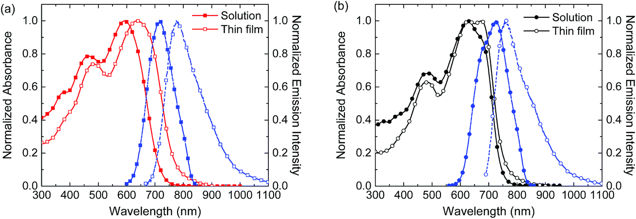 | ||
| Fig. 1 Normalized absorption (solid lines) and fluorescence (dashed lines) spectra in o-dichlorobenzene solution (solid markers) and thin films (open markers) for (a) PBDT4TBT and (b) PBDT4TffBT. | ||
| Polymer | λ abs,solmax (nm) | λ abs,filmmax (nm) | λ em,solmax (nm) | λ em,filmmax (nm) | E opt,filmg (eV) | E CVg (eV) | E HOMO (eV) | E LUMO (eV) |
|---|---|---|---|---|---|---|---|---|
| a Estimated from the onset of the lower energy band of the absorption spectrum. b Estimated as the difference between the onsets of the oxidation and reduction waves in the cyclic voltammogram. c E HOMO = −(5.23 + Eoxonset). d E LUMO = −(5.23 + Eredonset). | ||||||||
| PBDT4TBT | 593 | 637 | 718 | 775 | 1.62 | 1.78 | −5.28 | −3.50 |
| PBDT4TffBT | 625 | 673 | 726 | 762 | 1.65 | 1.91 | −5.42 | −3.51 |
The fluorescence spectra of the solutions of PBDT4TBT and PBDT4TffBT exhibit a single band (Fig. 1). The emission spectra of the corresponding films are broader and appear red-shifted. The (apparent) Stokes shift is smaller for PBDT4TffBT than for PBDT4TBT, both in solution (101 nm vs. 125 nm) and in the solid state (89 nm vs. 138 nm), suggesting a more ordered molecular structure for the fluorinated derivative.
The effect of temperature on conformation and aggregation was evaluated by recording the absorption spectra of o-dichlorobenzene solutions of PBDT4TBT and PBDT4TffBT. Fig. 2 reveals a markedly dissimilar temperature-dependent behavior. The absorption of PBDT4TBT (Fig. 2a) shows a gradual hypsochromic shift accompanied by a decrease of intensity with increasing temperature. The shift can be interpreted as a signature of a higher conformational flexibility of the polymer chains at higher temperature, while the intensity decrease is at least in part caused by expansion of the solvent. In contrast, for PBDT4TffBT, the shoulder assigned to the interchain π-aggregates gradually disappears at higher temperatures and there is a small, but distinct, increase of the absorption of molecularly dissolved chains at ∼540 nm (Fig. 2b). These changes are a consequence of a temperature-induced dissolution of polymer chains from aggregates at 20 °C towards molecularly dissolved non-planar chains at 100 °C. There is, however, no distinct isosbestic point because the spectral changes are a consequence of two temperature-dependent processes, i.e. aggregation and conformational flexibility. At 100 °C the absorption maxima of PBDT4TBT (542 nm) and PBDT4TffBT (536 nm) are almost identical.
 | ||
| Fig. 2 Temperature dependent absorption of (a) PBDT4TBT and (b) PBDT4TffBT in o-dichlorobenzene solution. Arrows indicate the heating direction. | ||
The redox potentials of the polymer films were determined using cyclic voltammetry (Fig. 3a). The voltammograms show two quasi-reversible reduction waves and one irreversible oxidation. The onsets of these redox waves were used to estimate the energies of the HOMO and LUMO levels (Table 1 and Fig. 3b). Both polymers have virtually the same LUMO energies but the HOMO level is lower for PBDT4TffBT (−5.42 eV) than for PBDT4TBT (−5.28 eV) as a consequence of the electronegative character of fluorine.
 | ||
| Fig. 3 (a) Cyclic voltammograms of thin polymer films on an ITO working electrode immersed in acetonitrile containing 0.1 M tetrabutylammonium hexafluorophosphate as the supporting electrolyte. The scan rate was 100 mV s−1, a Ag/AgCl electrode was used as the reference electrode and a silver rod as the counter electrode; (b) HOMO and LUMO energy levels. | ||
Photovoltaic properties
Solution processed bulk-heterojunction solar cells were fabricated by blending the polymers with [6,6]-phenyl-C71-butyric acid methyl ester ([70]PCBM) using a conventional device configuration consisting of a transparent indium tin oxide/poly(3,4-ethylenedioxythiophene):poly(styrene sulfonate) (ITO/PEDOT:PSS) front contact and a reflective LiF/Al back contact. The experimental details are provided in the Experimental section. The devices were optimized in terms of donor![[thin space (1/6-em)]](https://www.rsc.org/images/entities/char_2009.gif) :acceptor ratio, processing temperature, type and amount of solvent additives, and post-annealing treatment. Fig. 4a shows the current density–voltage (J–V) characteristics of the optimized devices under simulated air mass 1.5 (AM1.5) solar illumination and in the dark. The relevant photovoltaic parameters are listed in Table 2. PBDT4TffBT:[70]PCBM blends spin coated from o-dichlorobenzene provided higher short-circuit currents (JSC) than the PBDT4TBT:[70]PCBM blends (11.58 vs. 9.40 mA cm−2). Surprisingly, both polymers gave a comparable VOC, even though the fluorinated polymer has a 0.14 eV deeper HOMO level. The origin of this difference is studied and discussed in detail in the section “Charge recombination and charge transfer state” (vide infra). Hence, the difference in JSC accounts for the higher PCE of PBDT4TffBT (3.73%) compared to PBDT4TBT (2.82%). The higher photocurrent suggests a more favorable intermolecular arrangement or more intimate mixed morphology at the donor/acceptor interface for the fluorinated derivative.33
:acceptor ratio, processing temperature, type and amount of solvent additives, and post-annealing treatment. Fig. 4a shows the current density–voltage (J–V) characteristics of the optimized devices under simulated air mass 1.5 (AM1.5) solar illumination and in the dark. The relevant photovoltaic parameters are listed in Table 2. PBDT4TffBT:[70]PCBM blends spin coated from o-dichlorobenzene provided higher short-circuit currents (JSC) than the PBDT4TBT:[70]PCBM blends (11.58 vs. 9.40 mA cm−2). Surprisingly, both polymers gave a comparable VOC, even though the fluorinated polymer has a 0.14 eV deeper HOMO level. The origin of this difference is studied and discussed in detail in the section “Charge recombination and charge transfer state” (vide infra). Hence, the difference in JSC accounts for the higher PCE of PBDT4TffBT (3.73%) compared to PBDT4TBT (2.82%). The higher photocurrent suggests a more favorable intermolecular arrangement or more intimate mixed morphology at the donor/acceptor interface for the fluorinated derivative.33
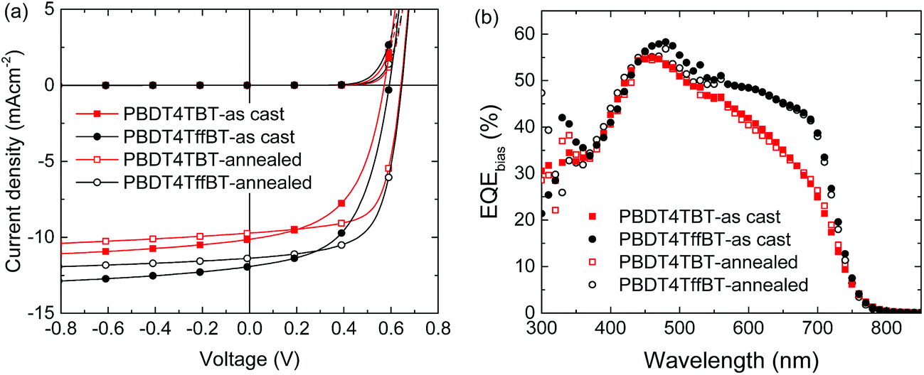 | ||
| Fig. 4 (a) Current density–voltage characteristics of solar cells in the dark and under simulated AM1.5G illumination. (b) EQE of the optimized devices. | ||
| Polymer | T (°C) | J SC (mA cm−2) | J SRSC (mA cm−2) | V OC (V) | FF | PCE (%) | PCEb (%) |
|---|---|---|---|---|---|---|---|
| a Calculated by integration of the EQE spectrum. b Based on JSRSC. | |||||||
| PBDT4TBT | n/a | 10.10 (10.00 ± 0.07) | 9.40 | 0.57 (0.57 ± 0.00) | 0.52 (0.50 ± 0.02) | 3.04 (2.87 ± 0.12) | 2.82 |
| PBDT4TBT | 200 | 9.72 (9.65 ± 0.08) | 9.35 | 0.64 (0.64 ± 0.00) | 0.68 (0.67 ± 0.01) | 4.23 (4.18 ± 0.04) | 4.06 |
| PBDT4TffBT | n/a | 11.90 (12.03 ± 0.10) | 11.58 | 0.59 (0.59 ± 0.00) | 0.54 (0.53 ± 0.01) | 3.84 (3.77 ± 0.05) | 3.73 |
| PBDT4TffBT | 150 | 11.40 (11.33 ± 0.10) | 10.64 | 0.65 (0.65 ± 0.00) | 0.65 (0.64 ± 0.01) | 4.74 (4.66 ± 0.10) | 4.44 |
Thermal annealing resulted in a distinct improvement in the PCE. For PBDT4TBT the VOC and FF continuously improve with annealing temperature, reaching a maximum at 200 °C, while JSC varies between 8.8 and 9.4 mA cm−2 in the same temperature range (Fig. 5a). The optimized thermally annealed (200 °C) device (PCE = 4.06%) outperforms the as-cast device (Table 2). For PBDT4TffBT, VOC and FF also increase with temperature, but JSC decreases continuously (Fig. 5b). The maximum PCE = 4.44% is reached after annealing at 150 °C (Table 2). Concomitant with an enhanced VOC, the built-in potential of the solar cells increases after thermal annealing (Fig. S13, ESI†).34 We notice that the HOMO and LUMO energies of polymer films as determined with cyclic voltammetry are the same within the experimental error, before and after the thermal treatment. The result that the photovoltaic parameters change with temperature is a consequence of a change in morphology, which affects the energy levels, charge generation, transport and recombination. The fact that the HOMO and LUMO levels of the pure polymer films do not change after annealing while the VOC shows a clear increase is consistent with our observation from X-ray diffraction that the blends with [70]PCBM show more pronounced changes, especially for PBDT4TBT, than the pure materials (vide infra). The external quantum efficiency (EQE) of the polymer blends reveals the contribution of both the donor and the acceptor to the photocurrent (Fig. 4b). The spectra are virtually identical below ∼500 nm and display a maximum EQE of 56% in the fullerene absorbing region (Fig. 4b). In the wavelength range where the polymers have their main absorption (500–780 nm), the EQE of PBDT4TffBT is higher than that of PBDT4TBT.
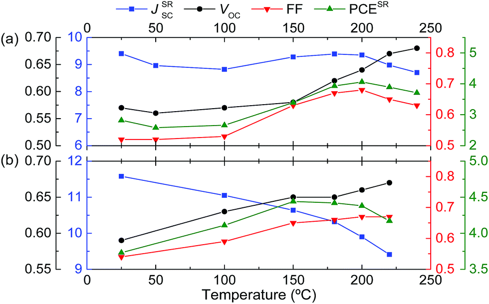 | ||
| Fig. 5 Evolution of the photovoltaic parameters with the annealing temperature for (a) PBDT4TBT and (b) PBDT4TffBT. | ||
Morphological characterization
The morphology of the blends was investigated to determine the origin of the differences in the device performance and the changes observed upon annealing. The absorption and photoluminescence spectra of the pristine polymers and the blends with [70]PCBM recorded before and after thermal annealing are shown in Fig. 6. Pure PBDT4TBT and PBDT4TffBT films exhibit small hypochromic and hyperchromic effects, respectively, while the band shape remains the same. In the blends with [70]PCBM, the effect of thermal annealing is very small for PBDT4TffBT, but more distinct for PBDT4TBT where annealing causes an increased absorption between 600 and 700 nm. In general, changes in absorption originate from changes in polymer planarization, aggregation and crystallization in combination with a possible change of the preferred order, but they can also be due to changes in the film thickness or refractive index. The overall changes are fairly small (<10%), which introduces the risk of over-interpreting the observed differences compared to experimental uncertainties. The increased absorption of the PBDT4TBT:[70]PCBM films after annealing is, however, consistent with the increased crystallization of these blends as inferred from the X-ray diffraction (vide infra). The small loss in absorption of the pure PBDT4TBT film after annealing and the gain in absorption for PBDT4TffBT are possibly related to a change in the preferred order. | ||
| Fig. 6 Absorption (a and b) and fluorescence (c and d) spectra of the as-cast (closed symbols) and annealed (open symbols) pristine polymer films and blends with [70]PCBM for (a–c) PBDT4TBT and (b–d) PBDT4TffBT. | ||
The fluorescence intensity of the pristine PBDT4TBT film decreases after annealing. We tentatively attribute this to the enhanced crystallinity after annealing (vide infra), which enhances the exciton diffusion rate, resulting in more trap quenching. For pristine PBDT4TffBT annealing does not really change the crystallinity (vide infra) and the very small increase can be due to the slightly higher absorption (Fig. 6b). The fluorescence in the blend films is significantly quenched compared to the pure polymers as a consequence of efficient exciton dissociation at the donor/acceptor interface (Fig. 6c and d). The residual emission of the polymers increased in intensity after annealing. This residual emission generally originates from excitons that are generated in larger pure polymer domains and do not reach the donor/acceptor interface. The higher intensity after annealing thus indicates that these pure polymer domains have increased in number or size.
The morphology of the blends was investigated by atomic force microscopy (AFM), transmission electron microscopy (TEM) and two-dimensional grazing incidence wide angle X-ray scattering (2D GIWAXS). The AFM images of the as-cast blends (Fig. 7a and c) show a very smooth surface topology with a root-mean-square roughness (Rq) of 0.67 nm for the PBDT4TBT:[70]PCBM blends and 0.75 nm for the PBDT4TffBT:[70]PCBM blends. In both cases, a rougher surface was found after the thermal annealing (Rq = 1.28 and 1.32 nm, Fig. 7b and d). Consistent with the AFM results, the TEM images of the post-annealed blends (Fig. 7f and h) revealed a slightly increased contrast, suggesting more pronounced phase separation, compared to those of the as-cast blends (Fig. 7e and g).
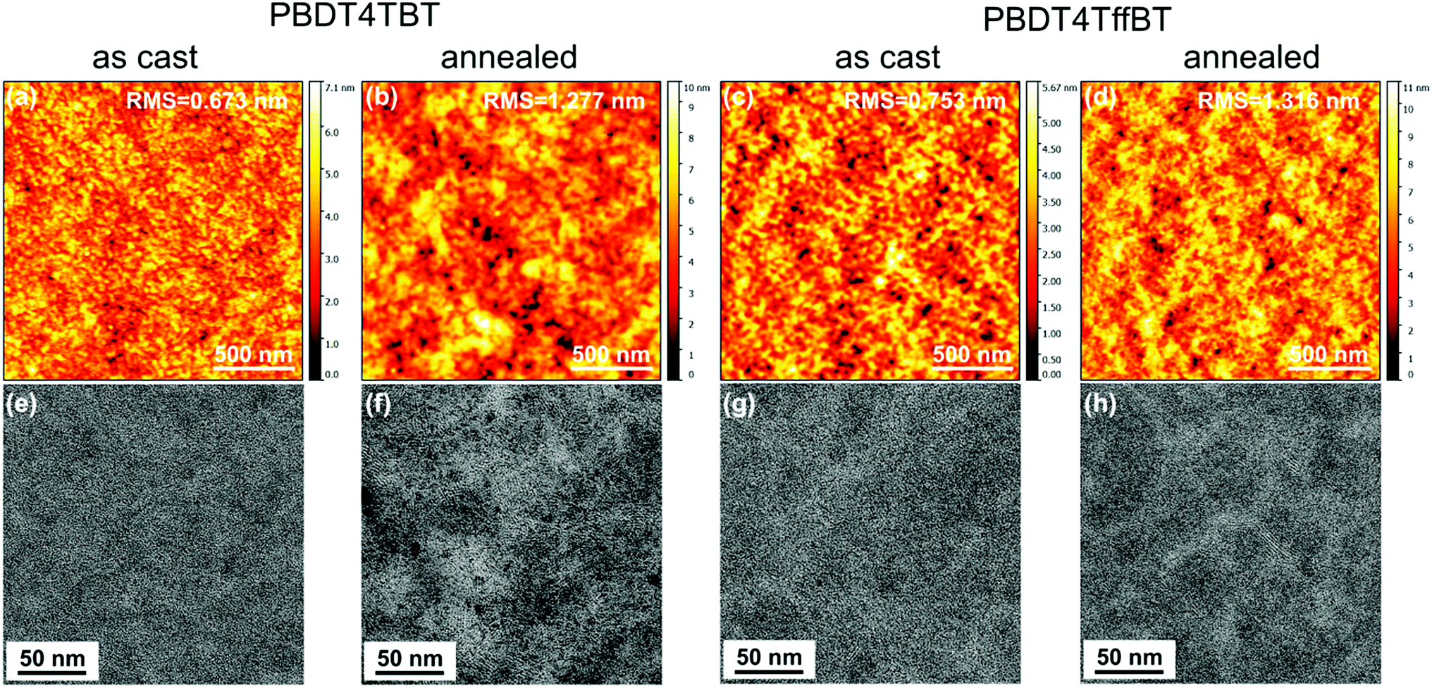 | ||
| Fig. 7 Tapping-mode AFM height (a–d) and TEM (e–h) images of the PBDT4TBT:[70]PCBM and PBDT4TffBT:[70]PCBM blends. | ||
The 2D GIWAXS patterns of the pristine PBDT4TBT and PBDT4TffBT polymers and their blends with [70]PCBM before and after thermal annealing are shown in Fig. S14 (ESI†). The corresponding line cut profiles for the out-of-plane and in-plane reflections are collected and shown in Fig. 8. The 2D-GIWAXS data confirm the main results inferred from optical absorption, fluorescence, J–V and EQE characteristics, AFM and TEM. For the pure as-cast films, PBDT4TBT shows less intense reflections than PBDT4TffBT (Fig. 8a and b), implying that it is less ordered. Thermal annealing has virtually no effect on the pure PBDT4TffBT films, but for the less ordered PBDT4TBT the intensity of the reflections increases slightly and a weak second order (200) reflection appears in the out-of-plane direction. The fluorinated polymer (PBDT4TffBT) has an almost perfect edge-on orientation showing (h00) reflections up to the 4th order (q100 = 0.302 Å−1, d100 = 20.8 Å) in the out-of-plane direction and a π–π stacking reflection (q001 = 1.765 Å−1, d001 = 3.56 Å) in the in-plane direction. In contrast, the non-fluorinated polymer (PBDT4TBT) has a less preferred orientation and shows a combination of edge-on and face-on arrangements with a slightly larger lamellar spacing (q100 = 0.280 Å−1, d100 = 22.4 Å) and π–π stacking (q001 = 1.758 Å−1, d001 = 3.58 Å) in the out-of-plane direction.
 | ||
| Fig. 8 Out-of-plane (a and c) and in-plane (b and d) line cut profiles from 2D-GIWAXS for pristine PBDT4TBT and PBDT4TffBT polymers and their blends with [70]PCBM before and after thermal annealing. | ||
In the blends with [70]PCBM the effects of thermal annealing are more pronounced, especially for the non-fluorinated polymer blend (PBDT4TBT:[70]PCBM); sharper and more reflections can be seen in both out-of-plane and in-plane directions for the lamellar spacing but also for the π–π stacking reflection in the in-plane direction. In this case also the reflections associated with [70]PCBM at q = 0.68 and 1.34 Å−1 increase in intensity and decrease in width. Similar, but less pronounced changes occur for the PBDT4TffBT:[70]PCBM blend. Overall the increased crystallinity after thermal annealing matches with the improved fill factors (FF, Table 2) because of better charge transport and with the more intense residual fluorescence because of the increased domain size, which is also reflected in a small loss in JSC (Table 2).
Summarizing, the absorption, fluorescence, AFM, TEM, and 2D-GIWAXS results are consistent with an increased aggregation of polymer chains after annealing in their blends with [70]PCBM. As a consequence exciton dissociation is decreased upon thermal annealing, resulting in a gradual loss of JSC. For PBDT4TBT this loss is partly compensated by an increased absorption due to aggregation (Fig. 6a). PBDT4TffBT cells do not profit from this effect, because the as-cast films are already aggregated (Fig. 6b).
Charge recombination and the charge transfer state
Charge carrier recombination was investigated by recording JSCvs. photon flux.35,36JSC follows a power law dependence on photon flux (Φ) expressed as follows:| JSC ∝ Φα | (1) |
| ηBR = 1 − EQEbias/EQEnobias | (2) |
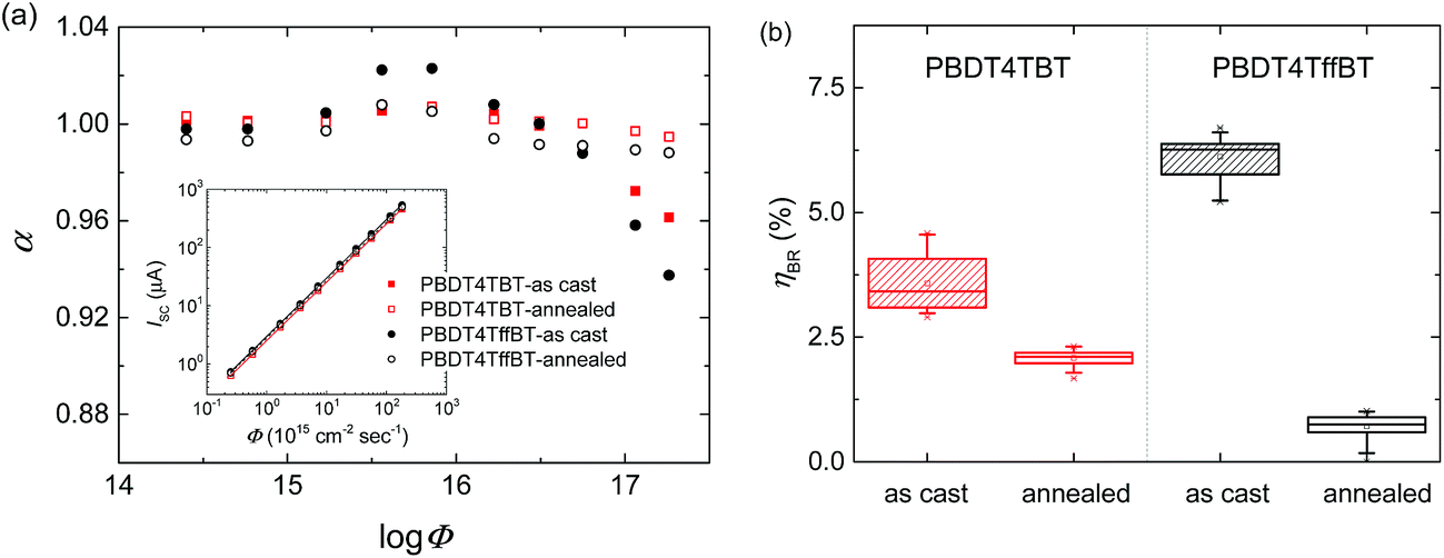 | ||
| Fig. 9 (a) First derivative of log(JSC) with respect to log(Φ) as a function log(Φ). Inset: double logarithmic plot of the short circuit current as a function of Φ for 530 nm photons. Lines correspond to the fits to a power law (eqn (1)). (b) Averaged bimolecular recombination loss efficiency estimated from EQEs using eqn (2), and 530 nm bias light. | ||
In concordance with the light intensity dependence studies, low averaged ηBR values were found (Fig. 9b). The bimolecular recombination was reduced upon thermal annealing for both polymer/fullerene blends from 4% to 2% for PBDT4TBT and from 6% to 1% for PBDT4TffBT. Such a decrease in the bimolecular recombination explains the improved VOC and FF of the annealed devices (Table 2).40,41
At open-circuit all charges recombine. To gain insight into the prevailing recombination mechanism at open circuit, the change in VOC with light intensity was investigated. The slope of VOCvs. light intensity in a semi-logarithmic plot gives the light ideality factor (nl) as a multiple of thermal energy (kT/q) (Fig. 10). For both polymers the VOC and nl increase upon thermal annealing. Generally, nl = 1 is associated with pure bimolecular recombination, while nl = 2 is characteristic of trap-assisted recombination in the bulk.42–44 We note, however, that trap-assisted surface recombination can also give rise to a low nl value.45 From the experiments shown in Fig. 9 we know that thermal annealing reduces bimolecular recombination, which results in an increase of VOC. The simultaneous increase of nl suggests that trap-assisted recombination becomes more dominant after annealing.
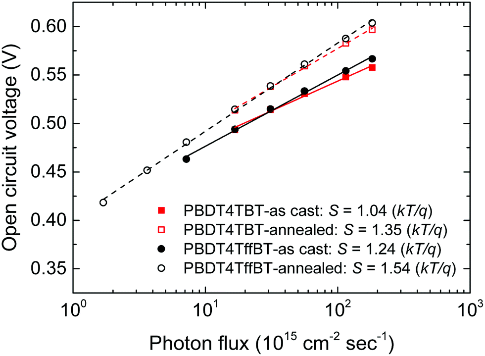 | ||
| Fig. 10 Semi-logarithmic plot of the open circuit voltage as a function of the incident light intensity. Lines correspond to the fits to a linear function. The slope in the legend is in units of kT/q. | ||
Dark ideality factors were calculated from the exponential region of the dark J–V curves (Fig. S15, ESI†) by using the expression ηd = [(kT/q)(dlnJ/dV)]−1. The dark ideality factors were larger than unity and moderately higher than the light ideality factors. We find good correspondence between both factors for the annealed devices.44–47
To understand the change in VOC after annealing, we also investigated the energy of the charge transfer state (ECT). It is experimentally well-established that VOC and ECT are linearly related. Hence variations in VOC can be better described by correlation with ECT than with the difference between the HOMO of the donor and the LUMO of the acceptor.5,12,48 Different methods and techniques have been employed to estimate ECT.49–52 Here we employ sensitive EQE and electroluminescence (EL) measurements to investigate the sub-gap region (Fig. 11).
 | ||
| Fig. 11 Normalized EQE (blue symbols) and EL (red and black symbols) spectra for the as-cast and annealed devices of (a and b) PBDT4TBT:[70]PCBM and (c and d) PBDT4TffBT:[70]PCBM. Dashed and solid lines correspond to the fits based on eqn (3) and (4) to the data. | ||
In the EQE measurements we see a considerable contribution of sub bandgap (<1.6 eV) states.53 As can be seen in Fig. 11, the distribution of sub bandgap states is wider for PBDT4TffBT than for PBDT4TBT and increases with thermal annealing. Based on Marcus theory,54 the band shape of the EQE and EL originating from the CT state can be described using the following expressions:11,15
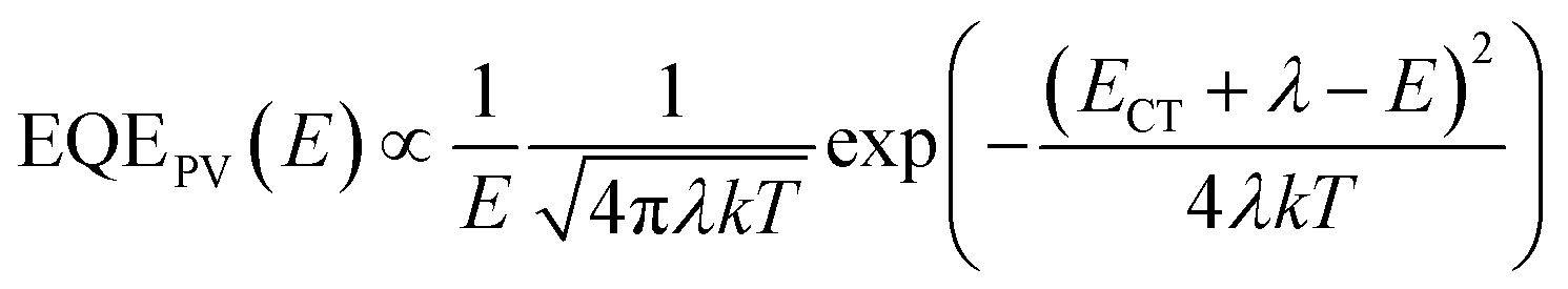 | (3) |
 | (4) |
Apart from EQE, EL allows to determine ECT and λ in an independent experiment. The EL spectra observed for the as-cast and thermally annealed PBDT4TffBT:[70]PCBM films (Fig. 11c and d) can be fitted to eqn (4), providing estimates for ECT and λ (Table 3). The same ECT and λ parameters should fit the EQE using eqn (3). The fits (dashed lines in Fig. 11c and d) show a reasonable correspondence with the experimental EQE, but also emphasize that additional low energy (<1.1 eV) states are present. For PBDT4TBT:[70]PCBM films, the situation is less clear and there is considerable uncertainty in the fitting. By simultaneously fitting the EQE and EL spectra we obtained only a fair agreement of the fits with the experimental data (Fig. 11a and b). Note that the absolute intensity of the EL of PBDT4TBT:[70]PCBM films was much less than that of PBDT4TffBT:[70]PCBM (Fig. S16, ESI†), such that the dark count rate raises the wings of the normalized spectrum.
| Polymer | Treatment | E CT (eV) | λ (eV) | qV OC (eV) | E CT − qVOC (eV) | E g − ECT (eV) |
|---|---|---|---|---|---|---|
| PBDT4TBT | As cast | 1.25 | 0.23 | 0.57 | 0.68 | 0.37 |
| PBDT4TBT | Annealed | 1.27 | 0.22 | 0.64 | 0.63 | 0.35 |
| PBDT4TffBT | As cast | 1.20 | 0.18 | 0.59 | 0.61 | 0.45 |
| PBDT4TffBT | Annealed | 1.23 | 0.19 | 0.65 | 0.58 | 0.42 |
The fluorinated polymer has lower ECT and λ than the non-fluorinated analogue (Table 3 and Fig. 11). The lower ECT for PBDT4TffBT is surprising because the HOMO energy of this polymer, determined from the oxidation potential, is lower than that of PBDT4TBT. The result can be rationalized by the fact that the fluorinated polymer is more ordered as can be inferred from the absorption spectra of the blends (Fig. 6a and b). Consistent with this explanation, the reorganization energy is also lower for the more ordered, fluorinated polymer. For both polymers ECT increases slightly after thermal annealing whereas λ remains virtually constant. Hence the CT states are affected by thermal annealing, but the increase in ECT is less than the increase in VOC. As a consequence the ECT − qVOC energy difference is reduced (Table 3), which indicates less non-radiative recombination. The absolute ECT − qVOC values of ∼0.6 eV obtained after annealing are consistent with the experimental values for many organic solar cells.15 Hence, the additional low energy (<1.1 eV) sub-gap states that can be seen in the EQE spectra (Fig. 11) of these polymers, seem not to affect the VOC considerably.
Conclusions
Two alternating BDT–4TBT copolymers have been synthesized that differ in the fluorine substitution on the BT unit. In bulk heterojunction solar cells, the fluorinated polymer exhibits a higher PCE. The performance of the as-cast devices was increased after thermal annealing at high temperatures (150–200 °C), by a distinct increase in VOC and FF, but a concomitant loss in JSC as a consequence of a more phase-separated blend morphology. After thermal annealing the dominant non-geminate charge recombination mechanism shifted from bimolecular or surface recombination to more trap-assisted recombination in the bulk. An analysis of the CT and reorganization energies revealed that a distribution of CT states exists. Surprisingly, the blends of the fluorinated polymer with [70]PCBM exhibited a lower CT state energy, despite its deeper HOMO level. The result can be rationalized by the fact that the fluorinated polymer is more ordered. Overall the ECT − qVOC energy difference is reduced after annealing.Although most results can be rationalized qualitatively, the data demonstrate that even a small structural modification, such as fluorination, can change the properties of these materials in a complex way where a subtle balance of electronic, conformational, and morphological changes determines the photovoltaic performance in a direction that is difficult to predict accurately. Solving this missing link remains a challenge for further progress of organic photovoltaics.
Experimental
Reagents used as starting materials and commercial solvents were used as received without further purification. Unless stated otherwise, all reactions were performed under an argon atmosphere. 1H NMR, 13C NMR and 19F NMR spectra were recorded on a Bruker spectrometer having frequencies of 400 MHz for proton nuclei, 100 MHz for carbon nuclei and 376.3 MHz for fluorine nuclei. Chemical shifts are given in ppm and were referred to the residual peak from the deuterated solvent. MALDI-TOF mass spectroscopy was performed on a Bruker Autoflex Speed spectrometer. Molecular weights and polydispersity index (PDI) were determined by gel permeation chromatography at 140 °C on a PL-GPC 120 system using a PL-GEL 10 μm MIXED-C column and o-dichlorobenzene as the eluent against polystyrene standards. The samples were stirred in o-dichlorobenzene at 140 °C for one hour before injection.Thermogravimetric analysis was carried out on a TA Instruments TGA Q500 instrument at a heating rate of 10 °C min−1 under nitrogen. Differential scanning calorimetry measurements were performed using a TA Instruments Q2000-1037 DSC with heating and cooling rates of 10 °C min−1 under nitrogen. The second heating run was analyzed. UV-vis-NIR spectroscopy was conducted on a Perkin Elmer Lambda 1050 spectrophotometer. Emission and electroluminescence spectra were recorded on an Edinburgh Instruments FLSP920 double-monochromator spectrophotometer equipped with a nitrogen cooled near-IR sensitive photomultiplier (Hamamatsu). The signals were corrected for the wavelength dependence sensitivity of the detection. Cyclic voltammetry was performed on thin films spin-coated on indium tin oxide (ITO) covered glass substrates under an inert atmosphere using an Autolab potentiostat with a scan speed of 0.1 V s−1 and 0.1 M tetrabutylammonium hexafluorophosphate in acetonitrile as the electrolyte. Ferrocene was used as the internal reference, ITO as the working electrode, a silver rod as the counter-electrode, and a Ag/AgCl electrode as the reference electrode.
For the photovoltaic device preparation pre-patterned ITO covered glass substrates (Naranjo Substrates), with an active area of 0.09 and 0.16 cm2, were cleaned by sonication in acetone, scrubbing and subsequent sonication with a sodium dodecyl sulfate solution, rinsing with demineralized water and finally, sonication in isopropanol for 15 minutes at each step. After 30 minutes of UV-ozone treatment, a thin layer (∼40 nm) of poly(3,4-ethylenedioxythiophene):poly(styrene sulfonate) (PEDOT:PSS) (Clevios P VP AI 4083) was spin-coated and annealed at 150 °C for 10 minutes. Then, the active layer consisting of a blend of the corresponding donor and [70]PCBM (1:1.5 by weight), which has been stirred at 90 °C overnight, was spin coated from the hot o-dichlorobenzene solution (8 mg mL−1). The layers were fully dried under vacuum immediately after spin coating for 10 minutes. Subsequently, the corresponding substrates were annealed in a hot plate for 5 minutes in a nitrogen filled glovebox. Finally, a 1 nm thick layer of LiF and a 100 nm thick layer of Al were thermally evaporated under high vacuum (∼3 × 10⁻⁷ mbar). The active layer thicknesses (∼100 nm) were measured with a Veeco Dektak 150 profilometer. J–V characteristics were measured with a Keithley 2400 source meter under ∼100 mW cm−2 white light illumination from a tungsten-halogen lamp filtered by a Schott GG385 UV filter and a Hoya LB120 daylight filter. Short-circuit currents under AM1.5G conditions were determined by integrating the spectral response with the solar spectrum. Spectral response measurements were conducted under 1 sun operating conditions by using a 530 nm high power LED (Thorlabs) for bias illumination. The device was kept in a nitrogen filled box behind a quartz window and irradiated with modulated monochromatic light, from a 50 W tungsten-halogen lamp (Osram 64610) and monochromator (Oriel, Cornerstone 130) with the use of a mechanical chopper. The response was recorded as a voltage from a preamplifier (SR570) using a lock-in amplifier (SR830). A calibrated silicon cell was used as a reference. For the high sensitivity EQE measurements the devices were irradiated with modulated monochromatic light, from a 250 W tungsten-halogen lamp (Osram 64655HLX) and monochromator (Oriel, Cornerstone 260). Besides, a calibrated InGaAs cell was also used as a reference. For the EL measurements a forward bias of 2.75 V was applied to the devices kept in a nitrogen filled box behind a quartz window in the same spectrometer as that used for the photoluminescence experiments. Light intensity measurements were performed at 530 nm using a high power LED (Thorlabs).
Atomic force microscopy (AFM) measurements were performed on an extended Veeco MultiMode AFM connected to a Nanoscope III controller in tapping mode using PPP-NCH-50 probes (Nanosensors). Transmission electron microscopy (TEM) was performed on a Tecnai G2 Sphera transmission electron microscope (FEI) operated at 200 kV.
The two-dimensional (2D) GIWAXS experiments were carried out on a GANESHA 300XL+ system from JJ X-ray in the X-ray lab at the DSM Materials Sciences Center (DMSC). The instrument is equipped with a Pilatus 300K detector, with a pixel size of 172 μm × 172 μm. The X-ray source is a Genix 3D Microfocus Sealed Tube X-ray Cu-source with an integrated monochromator (multilayer optic “3D version” optimized for SAXS) (30 W). The wavelength used is λ = 1.5408 Å. The detector moves in a vacuum chamber with the sample-to-detector distance varied between 0.115 and 1.47 m depending on the configuration used, as calibrated using silver behenate (d001 = 58.380 Å). The minimized background scattering plus high-performance detector allows for a detectable q-range varying from 3 × 10⁻³ to 3 Å−1 (0.2 to 210 nm). The sample was placed vertically on the goniometer and tilted to a glancing angle of 0.2° with respect to the incoming beam. A small beam was used to obtain sharper features in the scattering pattern. The primary slit has a size of 0.3 × 0.5 mm, and the guard slit has a size of 0.1 × 0.3 mm. The accumulation time was 6 h for each measurement. The data plot was constructed and data reduction was conducted using GIXSGUI and SAXSGUI programs.58
Conflicts of interest
There are no conflicts to declare.Acknowledgements
We thank Ms Fallon Colberts for the TEM images. M. M.-M. gratefully acknowledges the “Fundación Séneca, Agencia de Ciencia y Tecnología de la Región de Murcia” for a postdoctoral fellowship. The research has further received funding from the European Research Council under the European Union's Seventh Framework Programme (FP/2007–2013)/ERC Grant Agreement No. 339031 and from the Ministry of Education, Culture and Science (Gravity program 024.001.035).References
- National Renewable Energy Laboratory, N.R.E.L, http://www.nrel.gov/ncpv/images/efficiency_chart.png.
- R. A. J. Janssen and J. Nelson, Adv. Mater., 2013, 25, 1847–1858 CrossRef CAS PubMed.
- T. Linderl, T. Zechel, M. Brendel, D. M. González, P. Müller-Buschbaum, J. Pflaum and W. Brütting, Adv. Energy Mater., 2017, 7, 1700237 CrossRef.
- K. Kawashima, Y. Tamai, H. Ohkita, I. Osaka and K. Takimiya, Nat. Commun., 2015, 6, 10085 CrossRef CAS PubMed.
- K. Vandewal, A. Gadisa, W. D. Oosterbaan, S. Bertho, F. Banishoeib, I. V. Severen, L. Lutsen, T. J. Cleij, D. Vanderzande and J. V. Manca, Adv. Funct. Mater., 2008, 18, 2064–2070 CrossRef CAS.
- D. Veldman, S. C. J. Meskers and R. A. J. Janssen, Adv. Funct. Mater., 2009, 19, 1939–1948 CrossRef CAS.
- W. Li, K. H. Hendriks, A. Furlan, M. M. Wienk and R. A. J. Janssen, J. Am. Chem. Soc., 2015, 137, 2231–2234 CrossRef CAS PubMed.
- B. P. Rand, D. P. Burk and S. R. Forrest, Phys. Rev. B: Condens. Matter Mater. Phys., 2007, 75, 115327 CrossRef.
- T. M. Burke, S. Sweetnam, K. Vandewal and M. D. McGehee, Adv. Energy Mater., 2015, 5, 1500123 CrossRef.
- S. Chen, S.-W. Tsang, T.-H. Lai, J. R. Reynolds and F. So, Adv. Mater., 2014, 26, 6125–6131 CrossRef CAS PubMed.
- K. Vandewal, K. Tvingstedt, A. Gadisa, O. Inganäs and J. V. Manca, Phys. Rev. B: Condens. Matter Mater. Phys., 2010, 81, 125204 CrossRef.
- K. R. Graham, P. Erwin, D. Nordlund, K. Vandewal, R. Li, G. O. Ngongang Ndjawa, E. T. Hoke, A. Salleo, M. E. Thompson, M. D. McGehee and A. Amassian, Adv. Mater., 2013, 25, 6076–6082 CrossRef CAS PubMed.
- D. Fazzi, M. Barbatti and W. Thiel, J. Phys. Chem. Lett., 2017, 8, 4727–4734 CrossRef CAS PubMed.
- S. Kwon, H. Kang, J.-H. Lee, J. Lee, S. Hong, H. Kim and K. Lee, Adv. Energy Mater., 2017, 7, 1601496 CrossRef.
- K. Vandewal, Annu. Rev. Phys. Chem., 2016, 67, 113–133 CrossRef CAS PubMed.
- K. Vandewal, S. Albrecht, E. T. Hoke, K. R. Graham, J. Widmer, J. D. Douglas, M. Schubert, W. R. Mateker, J. T. Bloking, G. F. Burkhard, A. Sellinger, J. M. J. Fréchet, A. Amassian, M. K. Riede, M. D. McGehee, D. Neher and A. Salleo, Nat. Mater., 2014, 13, 63–68 CrossRef CAS PubMed.
- S. D. Collins, N. A. Ran, M. C. Heiber and T.-Q. Nguyen, Adv. Energy Mater., 2017, 7, 1602242 CrossRef.
- L. Dou, J. You, Z. Hong, Z. Xu, G. Li, R. A. Street and Y. Yang, Adv. Mater., 2013, 25, 6642–6671 CrossRef CAS PubMed.
- S. Xiao, Q. Zhang and W. You, Adv. Mater., 2017, 29, 1601391 CrossRef PubMed.
- X.-P. Xu, Y. Li, M.-M. Luo and Q. Peng, Chin. Chem. Lett., 2016, 27, 1241–1249 CrossRef CAS.
- N. Leclerc, P. Chávez, O. Ibraikulov, T. Heiser and P. Lévêque, Polymers, 2016, 8, 11 CrossRef.
- Q. Zhang, M. A. Kelly, N. Bauer and W. You, Acc. Chem. Res., 2017, 50, 2401–2409 CrossRef CAS PubMed.
- F. Meyer, Prog. Polym. Sci., 2015, 47, 70–91 CrossRef CAS.
- C. Duan, A. Furlan, J. J. van Franeker, R. E. M. Willems, M. M. Wienk and R. A. J. Janssen, Adv. Mater., 2015, 27, 4461–4468 CrossRef CAS PubMed.
- A. C. Stuart, J. R. Tumbleston, H. Zhou, W. Li, S. Liu, H. Ade and W. You, J. Am. Chem. Soc., 2013, 135, 1806–1815 CrossRef CAS PubMed.
- N. Wang, Z. Chen, W. Wei and Z. Jiang, J. Am. Chem. Soc., 2013, 135, 17060–17068 CrossRef CAS PubMed.
- I.-B. Kim, S.-Y. Jang, Y.-A. Kim, R. Kang, I.-S. Kim, D.-K. Ko and D.-Y. Kim, ACS Appl. Mater. Interfaces, 2017, 9, 24011–24019 CrossRef CAS PubMed.
- H. Yao, L. Ye, H. Zhang, S. Li, S. Zhang and J. Hou, Chem. Rev., 2016, 116, 7397–7457 CrossRef CAS PubMed.
- Y. Wang and T. Michinobu, J. Mater. Chem. C, 2016, 4, 6200–6214 RSC.
- H. Zhou, L. Yang, S. Xiao, S. Liu and W. You, Macromolecules, 2010, 43, 811–820 CrossRef CAS.
- A. Katsouras, N. Gasparini, C. Koulogiannis, M. Spanos, T. Ameri, C. J. Brabec, C. L. Chochos and A. Avgeropoulos, Macromol. Rapid Commun., 2015, 36, 1778–1797 CrossRef CAS PubMed.
- Z. B. Henson, K. Müllen and G. C. Bazan, Nat. Chem., 2012, 4, 699 CrossRef CAS PubMed.
- K. R. Graham, C. Cabanetos, J. P. Jahnke, M. N. Idso, A. El Labban, G. O. Ngongang Ndjawa, T. Heumueller, K. Vandewal, A. Salleo, B. F. Chmelka, A. Amassian, P. M. Beaujuge and M. D. McGehee, J. Am. Chem. Soc., 2014, 136, 9608–9618 CrossRef CAS PubMed.
- S. Solak, A. G. Ricciardulli, T. Lenz, N. I. Crăciun, P. W. M. Blom and G. A. H. Wetzelaer, Appl. Phys. Lett., 2017, 110, 163301 CrossRef.
- C. M. Proctor, M. Kuik and T.-Q. Nguyen, Prog. Polym. Sci., 2013, 38, 1941–1960 CrossRef CAS.
- G. Lakhwani, A. Rao and R. H. Friend, Annu. Rev. Phys. Chem., 2014, 65, 557–581 CrossRef CAS PubMed.
- S. R. Cowan, A. Roy and A. J. Heeger, Phys. Rev. B: Condens. Matter Mater. Phys., 2010, 82, 245207 CrossRef.
- I. Riedel, J. Parisi, V. Dyakonov, L. Lutsen, D. Vanderzande and J. C. Hummelen, Adv. Funct. Mater., 2004, 14, 38–44 CrossRef CAS.
- L. J. A. Koster, M. Kemerink, M. M. Wienk, K. Maturová and R. A. J. Janssen, Adv. Mater., 2011, 23, 1670–1674 CrossRef CAS PubMed.
- A. Maurano, R. Hamilton, C. G. Shuttle, A. M. Ballantyne, J. Nelson, B. O'Regan, W. Zhang, I. McCulloch, H. Azimi, M. Morana, C. J. Brabec and J. R. Durrant, Adv. Mater., 2010, 22, 4987–4992 CrossRef CAS PubMed.
- B. Qi and J. Wang, Phys. Chem. Chem. Phys., 2013, 15, 8972–8982 RSC.
- M. Lenes, S. W. Shelton, A. B. Sieval, D. F. Kronholm, J. C. Hummelen and P. W. M. Blom, Adv. Funct. Mater., 2009, 19, 3002–3007 CrossRef CAS.
- M. M. Mandoc, F. B. Kooistra, J. C. Hummelen, B. d. Boer and P. W. M. Blom, Appl. Phys. Lett., 2007, 91, 263505 CrossRef.
- S. R. Cowan, W. L. Leong, N. Banerji, G. Dennler and A. J. Heeger, Adv. Funct. Mater., 2011, 21, 3083–3092 CrossRef CAS.
- K. Tvingstedt and C. Deibel, Adv. Energy Mater., 2016, 6, 1502230 CrossRef.
- G. A. H. Wetzelaer, M. Kuik, M. Lenes and P. W. M. Blom, Appl. Phys. Lett., 2011, 99, 153506 CrossRef.
- T. Kirchartz, F. Deledalle, P. S. Tuladhar, J. R. Durrant and J. Nelson, J. Phys. Chem. Lett., 2013, 4, 2371–2376 CrossRef CAS.
- M. Gruber, J. Wagner, K. Klein, U. Hörmann, A. Opitz, M. Stutzmann and W. Brütting, Adv. Energy Mater., 2012, 2, 1100–1108 CrossRef CAS.
- Z. Guan, H.-W. Li, Y. Cheng, Q. Yang, M.-F. Lo, T.-W. Ng, S.-W. Tsang and C.-S. Lee, J. Phys. Chem. C, 2016, 120, 14059–14068 CrossRef CAS.
- F. E. Osterloh, M. A. Holmes, L. Chang, A. J. Moulé and J. Zhao, J. Phys. Chem. C, 2013, 117, 26905–26913 CrossRef CAS.
- K. Tvingstedt, K. Vandewal, A. Gadisa, F. Zhang, J. Manca and O. Inganäs, J. Am. Chem. Soc., 2009, 131, 11819–11824 CrossRef CAS PubMed.
- J. Behrends, A. Sperlich, A. Schnegg, T. Biskup, C. Teutloff, K. Lips, V. Dyakonov and R. Bittl, Phys. Rev. B: Condens. Matter Mater. Phys., 2012, 85, 125206 CrossRef.
- R. A. Street, A. Krakaris and S. R. Cowan, Adv. Funct. Mater., 2012, 22, 4608–4619 CrossRef CAS.
- R. A. Marcus, J. Phys. Chem., 1989, 93, 3078–3086 CrossRef CAS.
- A. N. Brigeman, M. A. Fusella, Y. Yan, G. E. Purdum, Y.-L. Loo, B. P. Rand and N. C. Giebink, Adv. Energy Mater., 2016, 6, 1601001 CrossRef.
- V. Belova, P. Beyer, E. Meister, T. Linderl, M.-U. Halbich, M. Gerhard, S. Schmidt, T. Zechel, T. Meisel, A. V. Generalov, A. S. Anselmo, R. Scholz, O. Konovalov, A. Gerlach, M. Koch, A. Hinderhofer, A. Opitz, W. Brütting and F. Schreiber, J. Am. Chem. Soc., 2017, 139, 8474–8486 CrossRef CAS PubMed.
- G. O. N. Ndjawa, K. R. Graham, S. Mollinger, D. M. Wu, D. Hanifi, R. Prasanna, B. D. Rose, S. Dey, L. Yu, J.-L. Brédas, M. D. McGehee, A. Salleo and A. Amassian, Adv. Energy Mater., 2017, 7, 1601995 CrossRef.
- Z. Jiang, J. Appl. Crystallogr., 2015, 48, 917–926 CrossRef CAS.
Footnote |
| † Electronic supplementary information (ESI) available. See DOI: 10.1039/c8ta03031f |
| This journal is © The Royal Society of Chemistry 2018 |