
 Open Access Article
 This Open Access Article is licensed under a
 Creative Commons Attribution 3.0 Unported Licence
Interdigitated back-contacted crystalline silicon solar cells with low-temperature dopant-free selective contacts†
G.
Masmitjà
 *,
P.
Ortega
,
J.
Puigdollers
,
L. G.
Gerling
,
I.
Martín
,
C.
Voz
and
R.
Alcubilla
*,
P.
Ortega
,
J.
Puigdollers
,
L. G.
Gerling
,
I.
Martín
,
C.
Voz
and
R.
Alcubilla
Department of Electronic Engineering, Universitat Politècnica de Catalunya (UPC), c/Jordi Girona 1-3, Mòdul C-4, 08034 Barcelona, Spain. E-mail: gerard.masmitja@upc.edu
First published on 26th January 2018
Abstract
In the field of crystalline silicon solar cells, great efforts are being devoted to the development of selective contacts in search of a fully low-temperature and dopant-free fabrication process compatible with high photovoltaic conversion efficiencies. For high-efficiency devices, selective contacts have to simultaneously combine high conductivity with excellent passivating properties. With this objective, a thin passivating extra layer of a-Si:H or SiO2 is usually introduced between the conducting layer and the silicon substrate. In this work, we present an interdigitated back-contacted (IBC) silicon based solar cell that avoids the use of either thermal SiO2 or a-Si:H interlayers achieving a dopant-free, ITO-free and very low thermal budget fabrication process. In this work, we propose a new electron transport layer using ultrathin Al2O3/TiO2 stacks deposited by atomic layer deposition at 100 °C covered with a thermally evaporated Mg capping film. A specific contact resistance of 2.5 mΩ cm2 has been measured together with surface recombination velocities below 40 cm s−1. This electron-selective contact is combined with a thermally evaporated V2Ox-based hole selective contact to form the rear scheme of an IBC structure with a 3 × 3 cm2 active area as a proof-of-concept resulting in efficiencies beyond 19%. This approach sheds light on potential technological simplification and cost reduction in crystalline silicon solar cells.
Introduction
Highly selective contacts to one type of carrier, i.e. passivated contacts, are necessary for high-efficiency solar cells. The function of such contacts is to block totally (ideally) or partially (in practice) one type of carrier, electrons or holes, while the other one is collected.1 Nowadays, the photovoltaic industry is mainly dominated by crystalline silicon (c-Si) solar cells, in which contact selectivity is usually achieved by doping the wafer surfaces with phosphorus (n+) and boron (p+) by means of high temperature oven-based diffusions, increasing either electron or hole conductivity. In this way, p+nn+ and n+pp+ doping schemes are a common way of achieving contact selectivity with n or p-type substrates, respectively. However, doping needs to be performed at high temperatures, requiring complex and energy consuming processes and lengthy cleaning protocols to avoid possible degradations of bulk lifetime, increasing the number of steps involved in the fabrication process and consequently the cost.In order to replace those high temperature diffusions, several approaches have been studied. The well-known silicon heterojunction (SHJ) structure using doped and intrinsic hydrogenated amorphous silicon (a-Si:H) films is probably the best known and combined with an interdigitated back-contacted (IBC) cell architecture holds the world efficiency record on c-Si substrates.2 Another low-temperature technology proposed is laser-doping where the p+ and n+ regions are formed by laser-processing of dielectric films.3,4 Nevertheless, both options use toxic and flammable gases as dopant precursors, which is not desirable from the point of view of process complexity.
A possible alternative arises from the heritage of thin film and organic photovoltaics, where novel materials are routinely used as semipermeable membranes to selectively extract carriers from a semiconductor light absorber.5 In this way, alternative materials that overcome conventional limitations and difficulties have been explored using the so-called DASH approach (Dopant Free Asymmetric Heterocontacts);6 materials such as organic polymers (PEDOT:PSS or P3HT),7,8 alkaline salts (LiFx, MgFx or Cs2CO3),6,9,10 transition metal oxides (TMOs)11 and multilayer TMO–metal–TMO12 have been successfully applied in c-Si solar cells as hole and electron transport layers (HTL and ETL respectively). This new paradigm broadens the technological possibilities and multiple options are being actively explored to achieve the best trade-off between efficiency and simplicity.13
In this context TMOs are becoming very attractive because of the combination of wide bandgaps (>3 eV) and consequently high transparency with low temperature deposition techniques, e.g. thermal evaporation, spin-on, spray-on and sputtering. High work-function TMOs (∼7 eV) such as molybdenum oxide (MoOx), tungsten oxide (WOx) and vanadium oxide (VOx) are preferred as hole-selective contacts,14 while low work-function compounds (∼4 eV) such as magnesium oxide (MgOx),15 lithium fluoride (LiFx)6 and titanium oxide (TiOx)16 are being investigated as electron-selective contacts.
Asymmetric conductivity in these materials is achieved either by band alignment or through a strong induced band-bending. In order to take advantage of the band structure of the silicon/contact interface while simultaneously decreasing surface recombination, it is important to avoid Fermi-level pinning by reducing the density of states at the silicon interface.17 In most cases, this is achieved by plasma enhanced chemical vapour deposition (PECVD) growth of a thin film of intrinsic a-Si:H between the TMO and the c-Si surface.6 Two drawbacks overshadow this approach, the use of flammable gases and the intrinsic difficulty of obtaining good Si/a-Si:H interfaces. Another possibility is to take advantage of the in situ redox reaction during thermal evaporation of the TMO material which may result in spontaneous growth of a SiOx film.18,19 Finally, some authors,20 although introducing a high temperature step, have grown a thin tunnel SiO2 layer between the TMO and the silicon surface.
Regarding electron-selective collector materials, TiO2-based contacts are an interesting alternative. Titania was firstly applied in c-Si photovoltaics as an antireflection coating,21 being an alternative to silicon-nitride or silicon oxide films. Recently, TiO2 films have begun to be used as a hole-blocking layer directly making contact with c-Si solar cells. However, poor contact passivation showing effective surface recombination velocities (Seff) of around 300 cm s−1 has limited the obtained efficiency to ∼11%.22 Interface recombination can be drastically reduced by growing an extremely thin thermal SiO2 layer at the interface between silicon and TiO2, where its thickness is the result of a trade-off between contact resistance and passivation. Using this approach for the preparation of the electron-selective contact along with conventional high temperature boron diffusion for the preparation of the hole-selective contact, a remarkable efficiency of 21.6% has been recently obtained for a double-side contacted solar cell.20 However, the high value of the contact resistance (>20 mΩ cm2) prevents the use of this approach in IBC structures where the electron contact area is only a fraction of the total rear surface.
The replacement of this passivation interlayer, e.g. thermal SiO2 or a-Si:H, by other films, which could be conformably deposited at low temperature with good thickness control, is an important research topic that may drastically simplify the fabrication process and reduce its cost. In this work, we focus on electron-selective contacts made of atomic layer deposited (ALD) TiO2 films combined with an ALD ultrathin Al2O3 interlayer. The Al2O3 is introduced between the TiO2 and the silicon surface aiming to reduce the defect density at the interface. In addition to Al2O3 and TiO2 thicknesses, the influence of different metal capping materials (Ni, Al and Mg) has been studied to optimize the selectivity. This Al2O3/TiO2 bilayer structure, or a repetition of it in nanolaminates, has been explored in the past for optical or gate dielectric applications.23,24 The passivation properties of this stack have been also reported,25 but it has not been previously applied and optimized as an electron-selective layer on c-Si solar cells, i.e. simultaneously targeting low surface recombination and contact resistance.
The best contact configuration consisting of a Mg-coated Al2O3/TiO2 stack is applied as an electron-selective contact on n-type c-Si solar cells. This ETL approach has not been reported in the literature on finished photovoltaic devices. In this paper, combining this new ETL concept together with a previously explored HTL stack (Ni-coated V2Ox),19 we report on highly efficient low-temperature and dopant-free n-type IBC c-Si solar cells with conversion efficiencies up to 19.1% on 9 cm2 devices. It is important to stress that both selective contacts (ETL and HTL) are fabricated at temperatures lower than 100 °C reducing the overall thermal budget of the fabrication process. Additionally the low resistivity values achieved using the ETL proposed herein allow us to circumvent the use of Indium Tin Oxide (ITO), further simplifying the fabrication process and eliminating the use of scarce materials.
Results and discussion
Surface contact passivation has been evaluated by extracting both the effective surface recombination velocity and the implicit open-circuit voltage (iVoc) from effective lifetime (τeff) measurements using the quasi-steady-state photoconductance decay technique (QSS-PC).26 Passivation test samples were fabricated on n-type float zone 〈100〉 c-Si substrates. One side was almost ideally passivated by means of a thick Al2O3 film (50 nm),19,27 allowing us to neglect the corresponding recombination in the effective lifetime measurements. The other side was covered with the Al2O3/TiO2 stack under investigation with different film thicknesses. Fig. 1 shows the iVoc values as a function of the number of Al2O3 and TiO2 ALD cycles, i.e. film thickness. Firstly, setting the number of Al2O3 ALD cycles to 3, 20 cycles of TiO2 seem to be the best choice from a passivation point of view, resulting in τeff and iVoc values of 660 μs (see ESI Fig. S1†) and 683 mV, respectively. Both increasing and decreasing the number of TiO2 cycles lead to a poorer surface passivation quality. This trend has already been reported by X. Yang et al.28 Secondly, when setting the number of TiO2 ALD cycles to 20, iVoc increases monotonically with the number of Al2O3 cycles achieving an iVoc value of 685 mV (Seff of 33 cm s−1) for 12 ALD cycles. Information about the Seff extraction can be found in the ESI.† Thus, we conclude that an Al2O3 interlayer between TiO2 and c-Si improves the passivation, increasing the iVoc from 667 to 687 mV as is also shown from an effective lifetime point of view in the ESI (Fig. S1†). Notice that no annealing is required to activate the passivation of the Al2O3/TiO2 stacks. It is also important to stress that surface passivation is stable up to a temperature of 250 °C as is shown in the ESI (Fig. S2†), which is enough to perform the following technological steps and a hypothetical encapsulation-lamination at 150 °C. | ||
| Fig. 1 Implied open circuit voltage (iVoc) values extracted from the measured effective lifetime (τeff) at different TiO2 and Al2O3 ALD cycles. (a) Study varying the number of TiO2 ALD cycles and fixing the number of ALD cycles for the Al2O3 film at 3. (b) Study varying the number of Al2O3 ALD cycles and fixing the number of ALD cycles for the TiO2 film at 20. Dashed lines are given as a guide to the eye. | ||
The excellent surface passivation provided by the ALD Al2O3 films is due to both chemical and physical passivation mechanisms.29 In other words, the silicon surface passivation when covered with Al2O3 originates on one hand from the low surface state density and simultaneously from the electric field effect due to the inherent charge in these films. In annealed Al2O3 films this charge is negative. However, it has been reported that relatively thick dielectric Al2O3/TiO2 stacks (∼20 nm) exhibit a net positive charge even after an annealing stage at 400 °C.30 Nevertheless, the details of the origin of surface passivation in ultra-thin conductive Al2O3/TiO2 structures and the passivation behaviour with annealing temperature are still unclear and further research in this field is required.
Although Al2O3/TiO2 stacks provide excellent surface passivation on n-type silicon substrates, good electron conduction properties are mandatory for electron-selective contacts. To check the contact quality and the influence of the metal capping on its electrical behaviour, test samples were fabricated on n-type c-Si substrates. The same Al2O3/TiO2 stacks were deposited on both sides of bare c-Si substrates. Then, one side was totally covered with the capping metal (Mg, Al or Ni) with a thickness of around 15 nm and finished with an extra 150 nm thick Al layer, whereas the other side was selectively metalized with the same electrode materials using a shadow mask in order to define dot features with different diameters (see the sketch in the inset of Fig. 2). The 150 nm thick Al layers are deposited without breaking the vacuum and serve to facilitate the measurements.
 | ||
| Fig. 2 (a) Impact of metal capping material on the measured dark current–voltage (I–V) characteristics using Al2O3/TiO2 stacks (6/20 ALD cycles) for 4 mm diameter spots. (b) Influence of the number of Al2O3 ALD cycles on I–V curves using Mg-coated samples (with 20 ALD cycles of TiO2). The test structure is depicted in the inset. In this case, 2 mm diameter spots were used. (c) I–V measurements of Mg-coated Al2O3/TiO2 stacks (6/20 ALD cycles) as a function of contact dot diameter. Contact resistance (ρc) extraction by fitting the total resistance (RT) curve through 3D simulations (dashed line) is shown in the inset. | ||
Semi-log I–V curves for a reference Al2O3/TiO2 stack (6/20 ALD cycles) with the different metal layers are shown in Fig. 2a. For a direct comparison, the I–V measurements were performed on dot features with the same pad diameter (4 mm) for all capping metals. The best behaviour corresponds to the sample in contact with Mg/Al achieving a low resistance ohmic curve with currents two orders of magnitude higher than that of the sample in contact with only Al. In contrast, the worst result is obtained for the sample in contact with Ni/Al, which results in a non-ohmic curve (see the asymmetric current level). Therefore, metal capping plays an important role in the functioning of the ETL structure. Note that depending on the metal material, the work function (φ) changes from a low to a high value (φMg ∼ 3.6 eV, φAl ∼ 4.3 eV and φNi ∼ 5.1 eV). The electrical contact quality improves with diminishing metal work function as expected in metal–semiconductor contacts on c-Si(n) substrates, i.e. the lower the work function value, the lower the contact barrier height, and the higher the majority carrier conduction through the silicon/contact interface. A similar behaviour has also been reported with a-Si:H passivated contacts using either Mg/Al or Al metal capping.31
In Fig. 2b the impact of the Al2O3 interlayer thickness ranging from 0 to 24 ALD cycles on the electrical contact quality is shown. In all cases, the thickness of the TiO2 layer was fixed at 20 ALD cycles and Mg/Al was used as a capping electrode. As we can see in this figure, for voltages from −1 to 1 V the characteristics are clearly ohmic for 0, 3, and even 6 ALD cycles. Nevertheless, this electrical behaviour changes to a poor ohmic contact for 12 ALD cycles, and exhibits a pseudo-rectifying I–V curve for the the case of 24 ALD cycles. This fact is in agreement with the dielectric nature of ALD Al2O3 films, which must finally block the electron-extraction, i.e. the tunnel conduction mechanism vanishes. Consequently, Al2O3 films prepared with 6 cycles (∼0.5 nm) yield the optimum trade-off between good passivation (thick films) and good electrical contact performance (thin films).
Fig. 2c shows the I–V curves for different dot-like contact diameters with the best stack configuration, Al2O3 (6 cycles)/TiO2 (20 cycles)/Mg. The specific contact resistance (ρc) of the stack can be extracted by fitting the measured total resistance (RT) for the different dot diameters using 3D simulations (Silvaco ATLAS TCAD).32 The results can be seen in the inset of Fig. 2c. Excellent ρc values of 2.5 ± 0.5 mΩ cm2 are obtained for our electron-selective contacts. Cumulative 5 min annealings have been performed showing stable results both for the specific contact resistance and for the iVoc up to 200 °C (see ESI Fig. S2†). This result improves ρc by more than one order of magnitude compared to SiO2/TiO2 stacks on n-type substrates.20 It is important to point out that small ρc values are crucial for manufacturing non-full contact high efficiency solar cells, in which the ETL coverage area fraction (fETL), defined as the ratio between ETL and total cell area, is typically in the 1–10% range. Considering that the specific series resistance (rs) is limited only by the ETL contact quality, the total series resistance could be roughly calculated as rs ≅ ρc × 100/fETL (%), yielding for the worst case (fETL = 1%) values below ∼0.3 Ω cm2 in final devices.
Finally, a single figure of merit quantifying contact quality is the so-called contact selectivity (S10) defined as S10 = log(Vth/(ρc × J0c)),33 where Vth is the thermal voltage (25.69 mV at 25 °C) and J0c is the contact recombination current density. This parameter is an alternative way to characterize surface recombination and can be calculated from the more common Seff concept (see the ESI† where a detailed explanation of this calculation can be found). Good contacts are characterized by simultaneously low ρc and J0c values. Thus, the higher the S10 value, the better the contact behaviour. Table 1 compares the main figures of merit reported in the literature for different ETLs. As can be observed, although the use of a thin a-Si:H(i) or alternatively a thermal SiO2 film as a passivating interlayer provides excellent surface passivation, these approaches usually exhibit poor conductivity, i.e. high contact resistance values. The ETL stack reported herein achieves a remarkable S10 value of 13.9, which is the best result for electron collector layers without using any PECVD or thermally grown passivation interlayer.
| ETL approach | iV oc (mV) | J 0c (fA cm−2) | S eff (cm s−1) | ρ c (mΩ cm2) | S 10 | Ref. |
|---|---|---|---|---|---|---|
| a Reported values related to contact passivation have been measured before LiFx deposition. b Extrapolated using the relationship J0c = Seff × qni2/ND from current Seff values, where ND, q and ni are the substrate doping, elementary charge and intrinsic concentration (ni = 8.56 × 109 cm−3 at T = 25 °C), respectively; see the ESI. c Measured in asymmetric test samples (one side ideally passivated). | ||||||
| a-Si:H(i) (6 nm)/LiFx (1 nm)/Al | 732a | 3a | — | 7 | 15.1 | 6 |
| MgOx (1 nm)/Al | — | — | — | 17.5 | — | 15 |
| Cs2CO3/Al | — | — | — | 61.8 | — | 9 |
| MgF2 (1 nm)/Al | 534 | 1500 | — | 35 | 8.7 | 9 |
| a-Si:H(i) (6.5 nm)/MgF2 (1 nm)/Al | 710 | 10 | — | 76 | 13.5 | 9 |
| TiO2 (2.5 nm)/Al | — | 132b | 56 | 20 | 10.0 | 20 |
| SiO2 (1.2 nm)/TiO2 (2.5 nm)/Al | — | 38b | 16 | 20 | 13.5 | 20 |
| TiO2 (3 nm)/Al/Ag | — | 3518b | 300 | — | — | 22 |
| Al2O3 (0.5 nm)/TiO2 (1.5 nm)/Mg/Al | 683c | 140b | 40 | 2.5 | 13.9 | This work |
In order to investigate the surface chemical composition of the reference Al2O3/TiO2 stack (6/20 ALD cycles), both uncoated and Mg-coated samples were analysed by the X-ray photoelectron spectroscopy (XPS) technique. In Fig. 3 the XPS analysis results of Si 2p, Ti 2p, and O 1s core levels for both samples are compared. In both cases, two peaks appear in the Si 2p spectrum (Fig. 3a). These peaks, which correspond to bulk Si and silicon oxide (Si–O) states, can be deconvoluted and fitted using Gaussian–Lorentzian curves centred at ∼99.0 and ∼102.0 eV binding energies, respectively. Since a HF dip was performed just before the ALD stack growth, oxidation of the Si surface might occur during the first water pulse in the Al2O3 deposition stage, where the Si dangling bonds react with oxygen. Additionally, ESI Fig. S3b† shows the Al 2p core level spectrum where the Al 2p3/2 peak centred at a binding energy of ∼74.2 eV confirms the existence of the alumina compound.
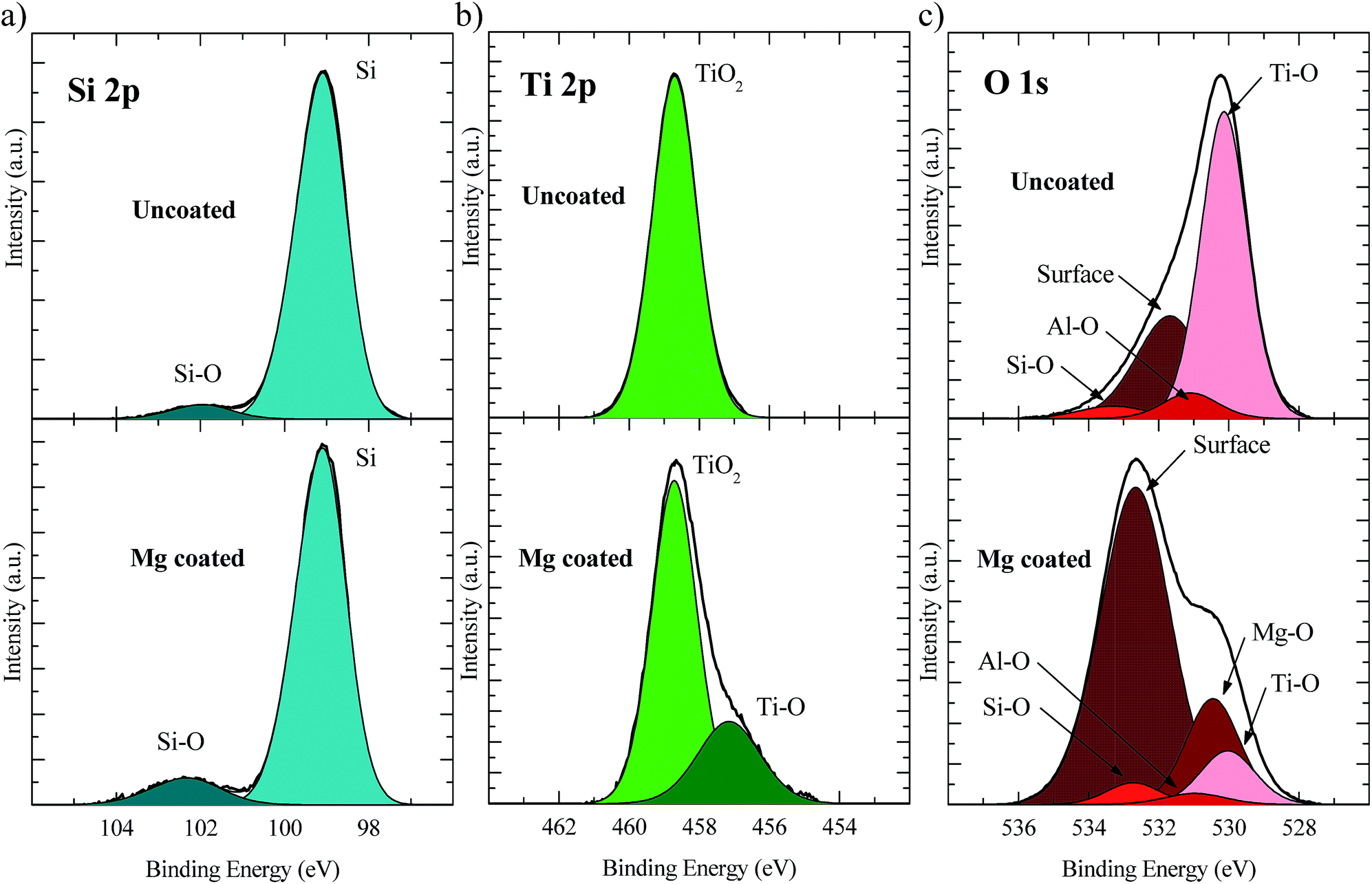 | ||
| Fig. 3 High-resolution XPS spectra of both uncoated and Mg-coated Al2O3/TiO2 stacks (6/20 ALD cycles) on n-type c-Si substrates. (a) Si 2p, (b) Ti 2p and (c) O 1s core levels spectra showing the multi-peak deconvolution of the fitted curves for different cation oxidation states. | ||
The Ti 2p3/2 core level spectrum is shown in Fig. 3b. For the uncoated sample, a single peak centred at a binding energy of ∼458.7 eV is enough to fit the curve. However, an extra peak centred at ∼457.1 eV appears for the Mg-coated sample. The peak at higher binding energy corresponds to a fully oxidized TiO2, while the lower binding energy peak is assigned to a titanium rich TiOx layer.24 From the relative area of the Ti–O peak with respect to the Ti 2p spectrum, an approximate TiOx content of 26% was calculated, indicating that only a fraction of the TiO2 layer is under-stoichiometric. The TMO work function changes strongly with the film stoichiometry,34i.e. oxygen-deficient layers exhibit lower work function values and a semi-metallic behaviour. In our devices, these effects might enhance the electron selectivity because of a proper band alignment and an improvement of layer conductivity. This oxygen deficiency could be attributed to a reaction of the thermally evaporated Mg with the TiO2, forming a magnesium oxide layer (MgOx). This hypothesis is corroborated by the Mg 2p spectrum, which exhibits a peak centred at a binding energy of ∼50.8 eV corresponding to an Mg–O compound (ESI Fig. S3a†).
Finally, an analysis of the O 1s core level spectrum (Fig. 3c) corroborates the presence of the many chemical species mentioned above. First, Al–O and Ti–O species (with a characteristic binding energy of ∼531.5 eV and ∼530.0 eV respectively) are identified in both samples, which correspond to the TiO2 and Al2O3 layers. However, the Mg-coated sample shows a smaller Ti–O intensity, attenuated by the Mg on top, as well as a Mg–O peak at 530.4 eV, confirming the presence of MgOx in the TiO2/Mg interface. An interesting feature is the detection of carbon contaminants adsorbed to the surface after air-exposure, whose contribution is particularly high for the Mg-coated sample (∼532.8 eV) and can be attributed to metal carbonate species, i.e. MgCO3.35 Also, the Si–O component (∼533.0 eV) is discernible for both samples.
In order to get a better insight into the influence of Mg on both the chemistry of Al2O3/TiO2 stacks and the electrical contact performance, we analysed their chemical composition using both energy dispersive X-ray spectroscopy (EDX) and electron energy loss spectroscopy (EELS) analysis. In Fig. 4a the high-angle annular dark field (HAADF) scanning transmission electron microscope (STEM) image reveals details of the contact structure. Firstly, a ∼15 nm thick Mg layer is observed as well as a ∼2 nm thick Al2O3/TiO2 stack. With the closer view shown in Fig. 4b, an Al2O3 interlayer (∼0.5 nm) was observed in the TiO2/c-Si interface capped with a ∼1.5 nm thick TiO2 layer. Due to the strong oxygen affinity of Mg metal, magnesium atoms easily attract oxygen atoms from the TiO2 interlayer forming an MgOx layer with a thickness of ∼2 nm. The existence of this extra layer is in agreement with the previous XPS measurements and confirmed by the EELS chemical composition cross scanning (see Fig. 4c). Interestingly, a similar behaviour was also observed when aluminium was evaporated directly onto TiO2 layers forming in this case an AlOx layer (see ESI Fig. S4†), in agreement with other reported studies.20 However, if Mg is used as a capping metal electrode, the spontaneous growth of a MgOx film may enhance the electron-selectivity of our contacts due to the already reported ETL nature of magnesium oxide.15
 | ||
| Fig. 4 (a) High-resolution STEM image of contact resistance test samples of a Mg-coated Al2O3/TiO2 stack (6/20 ALD cycles). (b) A close view of the Al2O3/TiO2/Mg stack. (c) EELS line scan confirming an MgOx interlayer grown in between TiO2 and Mg films. | ||
To demonstrate the viability of Al2O3/TiO2/Mg stacks as electron-selective contacts for c-Si solar cells, we fabricated a proof-of-concept 3 × 3 cm2 IBC structure on n-type c-Si substrates. The inset of Fig. 5a depicts the cell structure. The front-textured surface was covered with a 50 nm thick Al2O3 layer and further coated up to 75 nm with a close to stoichiometric silicon carbide layer (a-SiCx) providing excellent passivation as well as antireflection properties.36 It is important to point out that the gap between the interdigitated back-contacts is also passivated with the same stack. Therefore all non-contact surfaces are covered with a passivating and light confining Al2O3/SiCx stack which redirects light towards the bulk of the absorber and photogenerated carriers towards the corresponding contact.
 | ||
| Fig. 5 (a) EQE curve of the best IBC solar cell (fHTL/fETL = 52%/7% coverage values). A sketch of the device concept is shown in the inset. (b) Light J–V and pseudo light J–V curves for this IBC solar cell. The pseudo J–V characteristic, free of series resistance effects, is determined from Suns–Voc measurements. The dark J–V characteristic is depicted in the inset showing ideal exponential trends (lines) with ideality factors (n) of 1 and 2. | ||
External quantum efficiency (EQE) measurements for the best device are shown in Fig. 5a. EQE values close to 97% in the visible wavelength range confirm an excellent front and rear surface passivation pointing out that electron-selectivity in our ETL regions is good enough to obtain high photovoltaic efficiencies. Short circuit current densities (Jsc) of about 40 mA cm−2 and efficiencies (η) in the 18–19% range independently of the ETL coverage (fETL) have been measured, suggesting that surface passivation in the ETL regions is good enough to avoid excessive electrical shadowing.37 A similar high-efficiency structure has recently been reported combining a LiFx-based ETL and V2Ox–metal–V2Ox as the HTL in an IBC structure.12 However, in that device a high temperature phosphorus diffusion stage is needed to form a front surface field (FSF).
Details related to the photovoltaic parameters of the fabricated solar cells are listed in Table 2. Open circuit voltages (Voc) of up to 633 mV and fill factors (FF) of around 75% are achieved in our devices. Another interesting analysis is shown in Fig. 5b, where the illuminated current density–voltage (J–V) curve for the best IBC solar cell is compared with the corresponding pseudo-light J–V curve from Suns–Voc measurements.38 These measurements allow the determination of a pseudo J–V curve that excludes the series-resistance contribution. The matching between these two curves suggests that series resistance is not the limiting factor in the efficiency, as is corroborated by similar values of fill factor and pseudo-FF (pFF) parameters. The specific series resistance calculated using the relationship rs ≅ (1 − FF/pFF) × Voc/Jsc39 yields values below 0.4 Ω cm2 in all cases, confirming the high contact quality of our ETL stacks.
| Cell | f HTL/fETL (%) | J sc (mAcm−2) | V oc (mV) | FF (%) | pFF (%) | r s (Ωcm2) | η (%) |
|---|---|---|---|---|---|---|---|
| #1 | 40/8 | 39.4 | 631 | 76.4 | 77.1 | 0.144 | 18.9 |
| #2 | 52/7 | 40.0 | 633 | 75.4 | 76.3 | 0.183 | 19.1 |
| #3 | 64/5 | 39.2 | 633 | 76.0 | 77.9 | 0.398 | 18.8 |
| #4 | 76/3 | 39.4 | 625 | 74.1 | 76.9 | 0.391 | 18.2 |
The relatively low FF can be attributed to a diode ideality factor (n) close to two as can be seen in the dark J–V curve shown in the inset of Fig. 5b. This high n value might be attributed to poor coverage at the edges of the strip-like regions of the V2Ox-based HTL as is explained in detail in the ESI.† This drawback could be overcome in the future using the ALD technique to deposit both ETL and HTL selective contacts.
Conclusions
In this work, we apply atomic layer deposition of aluminium and titanium oxide (Al2O3/TiO2) stacks to form electron-selective contacts for interdigitated back-contacted n-type c-Si solar cells.The use of a very thin ALD Al2O3 passivation interlayer (∼0.5 nm) between silicon and the thin TiO2 film (∼1.5 nm) improves contact surface passivation, yielding surface recombination velocities below 33 cm s−1 and implicit open circuit voltages of about 680 mV in our test devices. Additionally, the metal capping layer plays an important role in contact conductivity, Mg being the best choice of material, with specific contact resistance values as low as 2.5 mΩ cm2 being reached. Chemical composition analysis (XPS and EELS) confirms spontaneous growth of a MgOx layer, leaving an oxygen-deficient TiOx layer in our Mg-coated samples.
Finally, the optimum electron-selective contact configuration consisting of an Al2O3 (6 ALD cycles)/TiO2 (20 ALD cycles)/Mg stack was applied to an interdigitated back-contacted solar cell structure using a V2Ox/Ni stack as a hole transport layer. In this way, fully TMO-based (9 cm2 area) solar cells reaching efficiencies up to 19.1% through a dopant-free and low-temperature fabrication process have been fabricated. These results outline the potential of TMOs to improve the trade-off between technological complexity and efficiency in Si solar cells.
Experimental
All the structures were fabricated using high quality 〈100〉 planar float zone (FZ) n-type c-Si wafers with a resistivity of 2 ± 1 Ω cm and a thickness of 280 ± 10 μm. The general trends of the IBC cell fabrication process have been described in a previous study.19 In this work the Al2O3/TiO2/Mg stack replaces laser doped contacts to create ETL regions. Therefore, fully low-temperature and dopant-free IBC solar cells based on TMOs have been fabricated. Photovoltaic parameters and illuminated J–V curves were measured under standard test conditions (1 kW m−2, AM1.5G solar spectrum, 25 °C) using an ORIEL 94021A (Newport) solar simulator. Light irradiance was properly calibrated by means of a pyranometer. The EQE curves were measured using a commercial instrument (QEX10, PV measurements) with a white light bias of 0.2 Suns and a beam spot of 2 × 2 cm2 centred within the active device area.The passivation test samples were subjected to a cleaning sequence of RCA1/2 (ref. 40) and a diluted HF (1%) dip prior to deposition at 200 °C on both sides of a 50 nm thick Al2O3 layer by ALD (Savannah S200, Cambridge Nanotech). Trimethylaluminium (TMA) and water were used as the aluminium precursor and oxidant species, respectively. A subsequent 10 min annealing was performed in forming gas (H2/N2) at 400 °C in order to activate the surface passivation provided by the Al2O3 films.27,36 Then, a 35 nm thick a-SiCx layer was deposited on one side by a plasma-enhanced chemical vapour deposition (PECVD) process (13.56 MHz, from Elettrorava S.p.A) at a temperature of 300 °C from silane (SiH4) and methane (CH4) precursor gases. This a-SiCx layer protects the films underneath against subsequent cleaning and HF dips. Finally, after a diluted RCA1-based cleaning41 and a HF (1%) dip to etch the thick alumina film (obtaining a hydrophobic surface), the Al2O3/TiO2 stack was deposited by ALD at 100 °C using the same ALD equipment. The stack was deposited without breaking the vacuum with an estimated growth rate of 1 Å per cycle and 0.63 Å per cycle for alumina and titania, respectively. The same alumina ALD precursors described above were used for the Al2O3 layers while tetrakis(dimethylamido)titanium(IV) (TDMAT) and water were used for depositing the TiO2 films. Note that while the thick Al2O3 passivating front layer needs a 10 min annealing at 400 °C, the annealing stage is not required for Al2O3/TiO2 stacks. Effective lifetime measurements were done by QSS-PC with a WCT-120 instrument (Sinton Consulting). The ESI (Fig. S6a†) shows the main technological steps involved in the fabrication of the test structures to analyse surface passivation.
Contact resistance test samples were subjected to a cleaning sequence of RCA1/2 and a diluted HF (1%) dip just before depositing the Al2O3/TiO2 stack by ALD with the same characteristics described above. An array of dot-patterned metal-pads with different diameters (0.5, 1, 2, and 4 mm) was evaporated on the front of the devices by means of a metallic shadow mask while the rear side was fully covered with the same metal used at the front. All metals were thermally evaporated from pure source materials >99.95% using a SQC-310 deposition controller (Sigma instruments). Metal films (Mg, Al or Ni) were ∼15 nm thick covered by a ∼150 nm thick Al layer. Evaporations were carried out in a vacuum chamber installed inside glovebox equipment (O2 < 0.1 ppm). The electrical measurements were performed using a four contact probe configuration by means of an I–V tracer (Keithley 3601B) at room temperature. The ESI (Fig. S6b†) shows the main technological steps involved in the fabrication of the contact resistance test structures.
The Al2O3/TiO2/Mg stack structure was studied by XPS using for the measurements a non-monochromatic Al-Kα source (1486.6 eV) at 3 × 10⁻⁹ mbar (SPECS, hemispherical energy analyser PHOIBOS 150). The thin films of Al2O3/TiO2 and Al2O3/TiO2/Mg were deposited on polished c-Si wafers immediately after a HF (1%) dip. High resolution images (HAADF-STEM) were acquired and both EDX and EELS chemical composition analyses were done using a Cs-corrected FEI Titan (60–300 kV) transmission electron microscope, equipped with a high brightness Schottky emitter source (X-FEG gun), a monochromator, and a Gatan 2k × 2k CCD camera. The cross-section lamellas were prepared from contact resistance test samples, using a focused ion beam (FIB) lift-out technique. Before the FEI Titan analysis, the samples were subjected to an O2 plasma cleaning.
Conflicts of interest
There are no conflicts to declare.Acknowledgements
This work has been supported partially by the Spanish Government under a FPU grant (FPU13/04381) and through projects ENE2016-78933-C4-1-R, TEC2014-59736-R, ENE2014-56237-C4-2-R and ENE2017-87671-C3-2-R. A part of the work is also supported by the project REFER COMRDI15-1-0036 funded by ACCIÓ and the European Regional Development Fund (FEDER). The authors wish to express their thanks to Dr R. Fernández-Pacheco and the Laboratorio de Microscopias Avanzadas (LMA-INA) facilities for SEM images and EELS/EDX analysis, as well as Dra M. Domínguez for her help and discussion about XPS measurements carried out at the Centre de Recerca en Ciència i Enginyeria Multiescala de Barcelona (CRCEMB).References
- U. Würfel, A. Cuevas and P. Würfel, IEEE Journal of Photovoltaics, 2015, 5, 461 CrossRef.
- K. Yoshikawa, H. Kawasaki, W. Yoshida, T. Irie, K. Konishi, K. Nakano, T. Uto, D. Adachi, M. Kanematsu, H. Uzu and K. Yamamoto, Nat. Energy, 2017, 2, 17032 CrossRef CAS.
- I. Martín, J. M. López-González, M. Colina, A. Orpella and R. Alcubilla, Proceedings of the 28th European Photovoltaic Solar Energy Conference and Exhibition (EU PVSEC), Paris, France, 2013, p. 1311 Search PubMed.
- P. Ortega, G. López, D. Muñoz, I. Martín, C. Voz, C. Molpeceres and R. Alcubilla, Sol. Energy Mater. Sol. Cells, 2017, 169, 107 CrossRef CAS.
- M. T. Greiner, M. G. Helander, W. –M. Tang, Z. –B. Wang, J. Qiu and Z. –H. Lu, Nat. Mater., 2012, 11, 76 CrossRef CAS PubMed.
- J. Bullock, M. Hettick, J. Geissbühler, A. J. Ong, T. Allen, C. M. Sutter-Fella, T. Chen, H. Ota, E. W. Schaler, S. De Wolf, C. Ballif, A. Cuevas and A. Javey, Nat. Energy, 2016, 1, 15031 CrossRef CAS.
- J. P. Thomas, L. Zhao, D. McGillivray and K. T. Leung, J. Mater. Chem. A, 2014, 2, 2383 CAS.
- F. Zhang, B. Sun, T. Song, X. Zhu and S. Lee, Chem. Mater., 2011, 23, 2084 CrossRef CAS.
- Y. Wan, C. Samundsett, J. Bullock, T. Allen, M. Hettick, D. Yan, P. Zheng, X. Zhang, J. Cui, J. McKeon, A. Javey and A. Cuevas, ACS Appl. Mater. Interfaces, 2016, 8, 14671 CAS.
- Y. Zhang, W. Cui, Y. Zhu, F. Zu, L. Liao, S.-T. Lee and B. Sun, Energy Environ. Sci., 2015, 8, 297 CAS.
- C. Battaglia, X. Yin, M. Zheng, I. D. Sharp, T. Chen, S. McDonnell, A. Azcatl, C. Carraro, B. Ma, R. Maboudian, R. M. Wallace and A. Javey, Nano Lett., 2014, 14, 967 CrossRef CAS PubMed.
- W. Wu, W. Lin, J. Bao, Z. Liu, B. Liu, K. Qiu, Y. Chen and H. Shen, RSC Adv., 2017, 7, 23851 RSC.
- C. Battaglia, A. Cuevas and S. De Wolf, Energy Environ. Sci., 2016, 9, 1552 CAS.
- L. G. Gerling, S. Mahato, A. Morales-Vilches, G. Masmitjà, P. Ortega, C. Voz, R. Alcubilla and J. Puigdollers, Sol. Energy Mater. Sol. Cells, 2016, 145, 109 CrossRef CAS.
- Y. Wan, C. Samundsett, J. Bullock, M. Hettick, T. Allen, D. Yan, J. Peng, Y. Wu, J. Cui, A. Javey and A. Cuevas, Adv. Energy Mater., 2017, 7, 1601863 CrossRef.
- S. Avasthi, W. E. McClain, G. Man, A. Kahn, J. Schwartz and J. C. Sturm, Appl. Phys. Lett., 2013, 102, 203901 CrossRef.
- R. T. Tung, Appl. Phys. Rev., 2014, 1, 011304 Search PubMed.
- L. G. Gerling, C. Voz, R. Alcubilla and J. Puigdollers, J. Mater. Res., 2017, 32, 260 CrossRef CAS.
- G. Masmitjà, L. G. Gerling, P. Ortega, J. Puigdollers, I. Martín, C. Voz and R. Alcubilla, J. Mater. Chem. A, 2017, 5, 9182 Search PubMed.
- X. Yang, Q. Bi, H. Ali, K. Davis, W. V. Schoenfeld and K. Weber, Adv. Mater., 2016, 28, 5891 CrossRef CAS PubMed.
- B. Liao, B. Hoex, A. B. Aberle, D. Chi and C. S. Bhatia, Appl. Phys. Lett., 2014, 104, 253903 CrossRef.
- K. A. Nagamatsu, S. Avasthi, G. Sahasrabudhe, G. Man, J. Jhaveri, A. H. Berg, J. Schwartz, A. Kahn, S. Wagner and L. C. Sturm, Appl. Phys. Lett., 2015, 106, 123906 CrossRef.
- B. G. Lee, J. Skarp, V. Malinen, S. Li, S. Choi and H. M. Branz, Proceedings of the 38th IEEE Photovoltaic Specialists Conference (PVSC), Austin, TX, 2012, p. 1066 Search PubMed.
- N. Y. Garces, D. J. Meyer, V. D. Wheeler, Z. Liliental-Weber, D. K. Baskill and C. R. Eddy Jr, J. Vac. Sci. Technol., B: Nanotechnol. Microelectron.: Mater., Process., Meas., Phenom., 2014, 32, 03D101 Search PubMed.
- D. Suh, D.-Y. Choi and K. J. Weber, J. Appl. Phys., 2013, 114, 154107 CrossRef.
- R. A. Sinton, A. Cuevas and M. Stuckings, Proceedings of the 25th IEEE Photovoltaic Specialists Conference (PVSC), Washington, DC, 1996, p. 457 Search PubMed.
- B. Hoex, S. B. S. Heil, E. Langereis, M. C. M. van de Sanden and W. M. M. Kessels, Appl. Phys. Lett., 2006, 89, 042112 CrossRef.
- X. Yang, P. Zheng, Q. Bi and K. Weber, Sol. Energy Mater. Sol. Cells, 2016, 150, 32 CrossRef CAS.
- B. Hoex, J. J. H. Gielis, M. C. M. van de Sanden and W. M. M. Kessels, J. Appl. Phys., 2008, 104, 113703 CrossRef.
- W.-C. Wang, M.-C. Tsai, J. Yang, C. Hsu and M.-J. Chen, ACS Appl. Mater. Interfaces, 2015, 7, 10228 CAS.
- Y. Wan, C. Samundsett, D. Yan, T. Allen, J. Peng, J. Cui, X. Zhang, J. Bullock and A. Cuevas, Appl. Phys. Lett., 2016, 109, 113901 CrossRef.
- ATLAS, http://www.silvaco.com/products/device_simulation/atlas.html.
- R. Brendel and R. Peibst, IEEE Journal of photovoltaics, 2016, 6, 1413 CrossRef.
- M. T. Greiner and Z.-H. Lu, NPG Asia Mater., 2013, 5, e55 CrossRef CAS.
- B. Vincent Crist, XPS Handbook of the Elements and Native Oxides, XPS International Inc., 1999 Search PubMed.
- G. López, P. Ortega, C. Voz, I. Martín, M. Colina, A. B. Morales, A. Orpella and R. Alcubilla, Beilstein J. Nanotechnol., 2013, 4, 726 CrossRef PubMed.
- C. Reichel, F. Granek, M. Hermle and S. W. Glunz, Progress in Photovoltaics: Research and Applications, 2013, vol. 21, p. 1063 Search PubMed.
- R. A. Sinton and A. Cuevas, Proceedings of the 16th European Photovoltaic Solar Energy Conference, Glasgow, UK, 2000, pp. 1–5 Search PubMed.
- M. A. Green, Solar Cells: Operating Principles, Technology and System Applications, University New South Wales, Kensington, F. S. W, Sydney, 1998, p. 96 Search PubMed.
- W. Kern, J. Electrochem. Soc., 1990, 137, 1887 CrossRef CAS.
- G. Masmitjà, P. Ortega, I. Martín, J. Pérez, G. López, E. Calle, L. G. Gerling, C. Voz and R. Alcubilla, Proceedings of the 11th Spanish Conference on Electron Devices (CDE), 2017, Barcelona, Spain, pp. 1–3 Search PubMed.
Footnote |
| † Electronic supplementary information (ESI) available. See DOI: 10.1039/c7ta11308k |
| This journal is © The Royal Society of Chemistry 2018 |