
 Open Access Article
 This Open Access Article is licensed under a Creative Commons Attribution-Non Commercial 3.0 Unported Licence
The effect of oxygen on the efficiency of planar p–i–n metal halide perovskite solar cells with a PEDOT:PSS hole transport layer†
Bardo J.
Bruijnaers
a,
Eric
Schiepers
a,
Christ H. L.
Weijtens
a,
Stefan C. J.
Meskers
 a,
Martijn M.
Wienk
a and
René A. J.
Janssen
*ab
a,
Martijn M.
Wienk
a and
René A. J.
Janssen
*ab
aMolecular Materials and Nanosystems, Institute for Complex Molecular Systems, Eindhoven University of Technology, P.O. Box 513, 5600 MB Eindhoven, The Netherlands. E-mail: r.a.j.janssen@tue.nl
bDutch Institute for Fundamental Energy Research, De Zaale 20, 5612 AJ, Eindhoven, The Netherlands
First published on 29th March 2018
Abstract
Poly(3,4-ethylenedioxythiophene):polystyrene sulfonate (PEDOT:PSS) is frequently used as hole transport layer in planar p–i–n perovskite solar cells. Here we show that processing of a metal halide perovskite layer on top of PEDOT:PSS via spin coating of a precursor solution chemically reduces the oxidation state of PEDOT:PSS. This reduction leads to a lowering of the work function of the PEDOT:PSS and the perovskite layer on top of it. As a consequence, the solar cells display inferior performance with a reduced open-circuit voltage and a reduced short-circuit current density, which increases sublinearly with light intensity. The reduced PEDOT:PSS can be re-oxidized by thermal annealing of the PEDOT:PSS/perovskite layer stack in the presence of oxygen. As a consequence, thermal annealing of the perovskite layer in air provides solar cells with increased open-circuit voltage, short-circuit current density and high efficiency.
Introduction
Metal halide perovskite materials currently attract great interest for use in hybrid organic–inorganic solar cells. Methylammonium lead halides were first used in 2009 as light sensitizers of mesoporous titania (TiO2) in photovoltaic cells comprising a liquid electrolyte, providing a power conversion efficiency (PCE) of 3.8%.1 The introduction of a solid organic hole transport material efficiently solved the fast degradation of the liquid-electrolyte cells and led to stable photovoltaic cells with an optimized PCE of 9.7%.2 The use of an insulating alumina (Al2O3) layer instead of the electron-transporting TiO2 layer proved that the perovskite material itself is capable of free charge generation and very efficient ambipolar charge transport.3 Recent advances have shown PCEs of over 22% for metal halide perovskites with optimized compositions and processing methods.4,5Metal halide perovskite materials possess many desirable properties like strong absorption, low exciton binding energy for creating free charges6–8 and high charge mobilities and lifetimes.9 The fact that metal halide perovskites can be processed from solution with relative ease makes future roll-to-roll processing an attractive option.10–12 Their versatility in composition and processing has allowed the usage of different solvents and precursor materials and even made it possible to tune the band gap of the material.13–23
Precursor and solvent combinations also allow the tuning of the morphology of the perovskite layer by influencing nucleation and crystal growth during the processing steps.24–27 The versatility in processing has led to many different processing techniques ranging from single-step solution processing,4,18 to multi-step solution processing with and without drying and anti-solvent treatments,28–31 single and multi-step thermal evaporation and even combinations of solution processing and thermal evaporation.32–36 After the deposition of the precursor materials, usually a (thermal) annealing step is used to convert the deposited layer into the desired perovskite phase and morphology.37–41 By changing the composition of the precursor solution, the crystallization process can be retarded or sped up and by combining different lead salt precursors, the layer can even be tuned to achieve a favourable morphology and smoothness of the perovskite layer for the most efficient solar cells, which is especially important in planar device configurations.24,26,42
Here we investigate the influence of the processing atmosphere on the photovoltaic performance of planar p–i–n perovskite solar cells with poly(3,4-ethylenedioxythiophene):polystyrene sulfonate (PEDOT:PSS) as hole transport layer, methylammonium lead triiodide as semiconductor and [6,6]-phenyl-C61-butyric acid methyl ester (PCBM) as electron transport layer. We show that the influence of the spin coating atmosphere on the PCE is negligible, while the annealing atmosphere has a marked effect. We found that the exposure to oxygen during thermal annealing of the perovskite layer is critical for obtaining efficient solar cells with high open-circuit voltage (VOC) and short-circuit current density (JSC). By annealing in an inert nitrogen atmosphere, these favourable characteristics cannot be achieved. We demonstrate that the optical and electronic properties in the bulk of the perovskite layer are independent of the annealing atmosphere. Instead, a chemical reduction of the oxidation state of the PEDOT:PSS layer during the deposition of the perovskite precursor is the cause of the decreased photovoltaic performance of devices. This chemical reduction lowers the work function of the PEDOT:PSS and of the perovskite layer on top of it, reducing the built-in voltage of the cell and leading to a lower VOC. The JSC is further reduced due to surface recombination, which causes a significant sublinear light intensity dependence of JSC and of the external quantum efficiency (EQE) of cells annealed in nitrogen. By thermal annealing in the presence of oxygen, it is possible to restore the oxidation state and work function of PEDOT:PSS and obtain high efficient devices.
Results and discussion
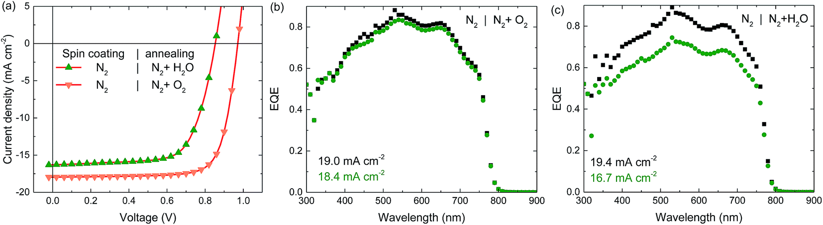
The perovskite solar cell fabrication is based on a triple anion solution of methylammonium iodide (MAI), lead(II) chloride (PbCl2) and lead(II) acetate (Pb(OAc)2) in N,N-dimethylformamide (DMF). This solution is heated to 70 °C and spin coated dynamically onto a pre-heated (100 °C) glass substrate with patterned indium tin oxide (ITO), covered with PEDOT:PSS. By this hot-casting method the very hygroscopic precursor salts are already converted to the perovskite during deposition, as indicated by a pronounced colour change from the yellow precursor to the brown perovskite. Even though perovskite crystals are already formed during casting, a short additional thermal annealing step, during which the colour of the perovskite layer changes from light brown to dark brown, is required to maximize the efficiency.42 The devices are completed by a PCBM electron transport layer and a LiF/Al contact. Further details of the fabrication can be found in the Experimental.Fig. 1a shows the stabilized current density–voltage (J–V) measurements under simulated AM1.5G (100 mW cm−2) illumination of these p–i–n photovoltaic devices, when all processing steps are either done in ambient air or in an inert N2 atmosphere. The corresponding photovoltaic parameters are summarized in Table 1. Strikingly, the efficiency of cells processed under inert conditions (N2 atmosphere, < 1 ppm O2 and < 1 ppm H2O) is much lower than the PCE of the air-processed device where both JSC and VOC are considerably enhanced.
 | ||
| Fig. 1 Stabilized current density–voltage (J–V) curves (a and d) under simulated AM1.5G illumination, and EQE spectra (b, c, e and f) of ITO/PEDOT:PSS/perovskite/PCBM/LiF/Al solar cells processed under different atmospheres as indicated in the legends. Black squares depict the EQE under low charge carrier density (i.e. without bias illumination), green circles depict the EQE at a charge carrier density similar to that of the cell under 1 sun light intensity (i.e. with bias illumination). The integrated current density is displayed in the graphs for both measurements. The dark J–Vs belonging to panel (a) are displayed in the ESI, Fig. S1.† | ||
| Spin coating atmosphere | Annealing atmosphere | Perovskite thickness (nm) | J SC, J–V (mA cm−2) | J SC, SR@1 sun (mA cm−2) | V OC (V) | FF | PCEa (%) |
|---|---|---|---|---|---|---|---|
| a The PCE has been calculated with the photocurrent determined from integrating the EQE spectrum with the AM1.5G spectrum (JSC, SR@1 sun). | |||||||
| Air | Air | 401 | 17.1 | 18.0 | 0.99 | 0.78 | 14.0 |
| Air | N2 | 409 | 15.2 | 14.9 | 0.94 | 0.77 | 10.9 |
| N2 | N2 | 399 | 15.0 | 15.8 | 0.92 | 0.76 | 11.8 |
| N2 | Air | 380 | 17.5 | 18.8 | 0.96 | 0.78 | 14.2 |
| N2 | N2 + O2 | 368 | 18.0 | 18.4 | 0.97 | 0.76 | 13.7 |
| N2 | N2 + H2O | 377 | 16.3 | 16.7 | 0.85 | 0.70 | 9.9 |
To identify which processing step, deposition or annealing, is most critical, devices partially processed in air and N2 have been measured (Fig. 1d). For cells deposited in N2 but annealed in air the performance is almost identical to the fully air processed device. In sharp contrast, cells cast in air but annealed in N2, resemble the fully N2-processed devices. This demonstrates that the annealing atmosphere, and not the casting atmosphere, has the largest impact on the performance.
The significantly lower JSC for cells annealed in N2 was confirmed by EQE measurements under appropriate 1 sun equivalent bias light (Fig. 1b, c, e and f). Remarkably, in absence of bias light the magnitude of the EQEs of the N2-annealed cells is much higher and similar to that of the air-annealed cells. Indicating that for the samples annealed in N2 charge carrier collection is only reduced at higher charge carrier densities created by high illumination intensities.
Scanning electron microscopy (SEM) images of the top surface of the four differently processed perovskite layers (Fig. 2) indicate that the largest morphological differences can be related to the casting atmosphere. Perovskite layers cast in air possess smaller crystallites compared to those cast in N2. This could be related to a more efficient perovskite nucleation, probably due to the presence of moisture in the air.43 The distinct difference in morphology, however, does not significantly affect the device performance. The X-ray diffractograms (XRD) (Fig. 3) of these four samples are very similar, showing the same degree of preferential orientation and the presence of a small PbI2 peak for all samples. X-ray photoelectron spectroscopy (XPS) analysis on perovskite layers spin coated in N2 and annealed in either air or N2 do not show any difference in the composition of the perovskite layers and the calculated atomic Pb![[thin space (1/6-em)]](https://www.rsc.org/images/entities/char_2009.gif) :I ratio is 1:3 (Fig. S2, ESI†).
:I ratio is 1:3 (Fig. S2, ESI†).
 | ||
| Fig. 2 Scanning electron microscopy (SEM) top view images of perovskite layers spin coated in air or N2 using the hot cast method and annealed in air or N2 as indicated above the images (scale bars are 1 μm). | ||
 | ||
| Fig. 3 X-Ray diffractograms of perovskite layers spin coated in air or N2 using the hot cast method and annealed in air or N2. The inset is a zoom and shows the presence of a small PbI2 peak at ∼12.8°. | ||
Experiments so far demonstrate that exposure to air during annealing of the perovskite layer is beneficial for the device performance. Besides N2, ambient air contains oxygen and moisture, both of which have been shown to impact the properties of perovskite layers.39,43–45 To identify which component is of importance here, experiments were conducted in which the perovskite annealing in dry air (i.e. exposure to O2 but not to H2O) was compared to annealing in humid N2 (i.e. exposure to H2O but not to O2). Spin coating was done in N2 in both cases since this provides more stability of the un-annealed samples over time when stored in N2 after spin coating (Fig. S3 and S4, ESI†). The perovskite layer annealed in humid N2 performs very similar to the one annealed in dry N2, displaying both a low VOC and JSC, and a pronounced light intensity dependent EQE, indicating that water does not significantly influence the annealing process (Fig. 4a and c). The perovskite layer annealed in dry air however, performs very similarly to layers annealed in ambient air, generating a high voltage and current, and a light-intensity independent EQE (Fig. 4a and b). This demonstrates that the oxygen content of the air is the main reason for the performance increase. Table 1 summarizes the stabilized photovoltaic characteristics of these perovskite solar cells.
 | ||
| Fig. 4 Stabilized J–V curves (a) and EQE spectra (b and c) of perovskite solar cells spin coated in N2 using the hot cast method and annealed in dry air and humid N2 as indicated in the legends. Black squares depict the EQE under low charge carrier density (i.e. without bias illumination), green circles depict the EQE at a charge carrier density similar to that of the cell under 1 sun light intensity (i.e. with bias illumination). The integrated current density is displayed in the graphs for both measurements. | ||
It is important to note that described sensitivity to oxygen during annealing is not exclusive to the hot-cast deposited perovskite layers. Identical results have been obtained for perovskite films deposited using a much more commonly used static casting at room temperature under inert circumstances. Also in this case films that are annealed in absence of oxygen show low VOC and JSC and bias light dependent EQEs (Fig. S5–S7 and Table S1, ESI†).
Light intensity dependent JSC measurements (Fig. 5a) show that the current generation of the N2-annealed samples is more sublinear (JSC ∝ Iα, with α < 1) than that of air-annealed samples. Especially at higher light intensities the exponent α starts deviating from 1, consistent with the results from the EQE measurements. From the light intensity dependent VOC measurement (Fig. 5b), the ideality factor (n) is calculated by determining the slope of the VOCversus the logarithm of the light intensity in the linear part of the graph,46–48 where a slope equal to the thermal voltage (−kT/q with k the Boltzmann constant, T the absolute temperature, and q the elementary charge) represents an ideality factor of 1. An ideality factor of n = 2 indicates dominant trap-assisted recombination in the bulk, an ideality factor of 1 indicates purely bimolecular recombination. The higher slope at low light intensities is caused by recombination over shunt paths.48 The ideality factor determined using this method is about n ≈ 1.3 for air-annealed cells, which would indicate a significant amount of trap-assisted (Shockley–Read–Hall (SRH)) recombination. The ideality factor of the N2-annealed cells, however is about n ≈ 1, which would suggest pure bimolecular recombination. However, the VOC of this cell is lower than that of the air annealed cell, which should not be the case for an identical device with an ideality factor closer to unity. Strong surface recombination at a doped interface however, can reduce the ideality factor, making it appear to be closer to unity.49 Additionally, VOCvs. light intensity measurements using different illumination wavelengths (405 nm absorbed predominantly in the first 100 nm of the active layer seen from the PEDOT:PSS layer and 730 nm absorbed more uniformly through the active layer) show that the charge carrier generation profile inside the perovskite layer does not strongly influence the VOC or the ideality factor. Together, these results suggest that the PEDOT:PSS/perovskite interface is a source of significant surface recombination in the N2-annealed perovskite cell at higher light intensities.48,50,51
 | ||
| Fig. 5 (a) Light intensity dependent JSC of air-annealed (blue solid squares) and N2-annealed (red solid circles) perovskite solar cells (using an illumination wavelength of 730 nm). A black line with an exponent α = 1 is added as a visual aid. (b) Light intensity dependent VOC of air annealed (blue squares) and N2 annealed (red circles) perovskite solar cells measured using two different illumination wavelengths (730 nm solid symbols and 405 nm open symbols). The ideality factors (n) calculated from the slopes of linear fit lines to the higher light intensity linear parts of the curves are n ≈ 1 for N2-annealed cells and n ≈ 1.3 for air-annealed cells. | ||
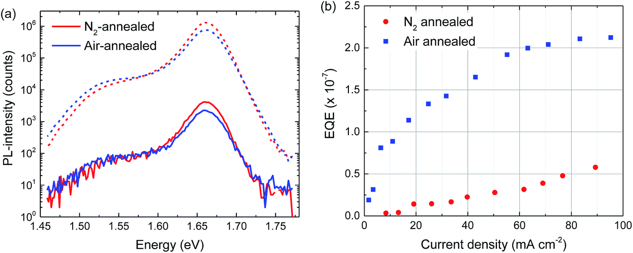
As a next step, photoluminescence (PL) and electroluminescence (EL) measurements were conducted on air-annealed and N2-annealed layers and devices respectively. If the interface is indeed defective, the PL measurements should provide similar results for the air- and N2-annealed layers since the interfaces are not probed. In contrast, the EL measurements can show differences between the air- and N2-annealed perovskite cells, when charges build up near the injecting charge transport layers.
Room temperature and low temperature (70 K) photoluminescence results yield very similar results for the air- and N2-annealed perovskite layers (Fig. S8–S11, ESI†). At room temperature the PL is dominated by a band at 1.60 eV, while at 70 K the emission peaks at 1.66 eV together with a weak trap-related emission at 1.53 eV (Fig. 6a). At 70 K there is no significant difference in peak shape and position at both medium and low illumination intensities and the relative intensity of the 1.53 eV defect emission does not seem to increase (Fig. 6a). Electroluminescence external quantum efficiency (EL-EQE) measurements at room temperature show that the EL-EQE of perovskite layers annealed in air is higher than that of perovskite layers annealed in nitrogen (Fig. 6b), which holds up to high current densities (>100 mA cm−2). Because the current through the perovskite cells is similar for both annealing atmospheres (Fig S12, ESI†), Fig. 6b indicates that the air-annealed cells show electroluminescence at lower voltages, consistent with less traps that need to be filled before charges can recombine radiatively. In EL measurements at different voltages at room temperature and 70 K, no significant differences could be found in peak shape and position (Fig. S13, ESI†).
 | ||
| Fig. 6 (a) Photoluminescence spectra at 70 K of perovskite layers annealed in air (blue) and nitrogen (red) at high (dashed lines) and low (solid lines) illumination intensities. (b) EL-EQE measurements of solar cells with perovskite layers annealed in air (blue solid squares) and N2 (red solid circles). | ||
Combining the room- and low-temperature PL and EL results, we conclude that the improvement of the solar cell performance in the air-annealed perovskite layers is not primarily due to a change in the bulk properties of the perovskite layer.
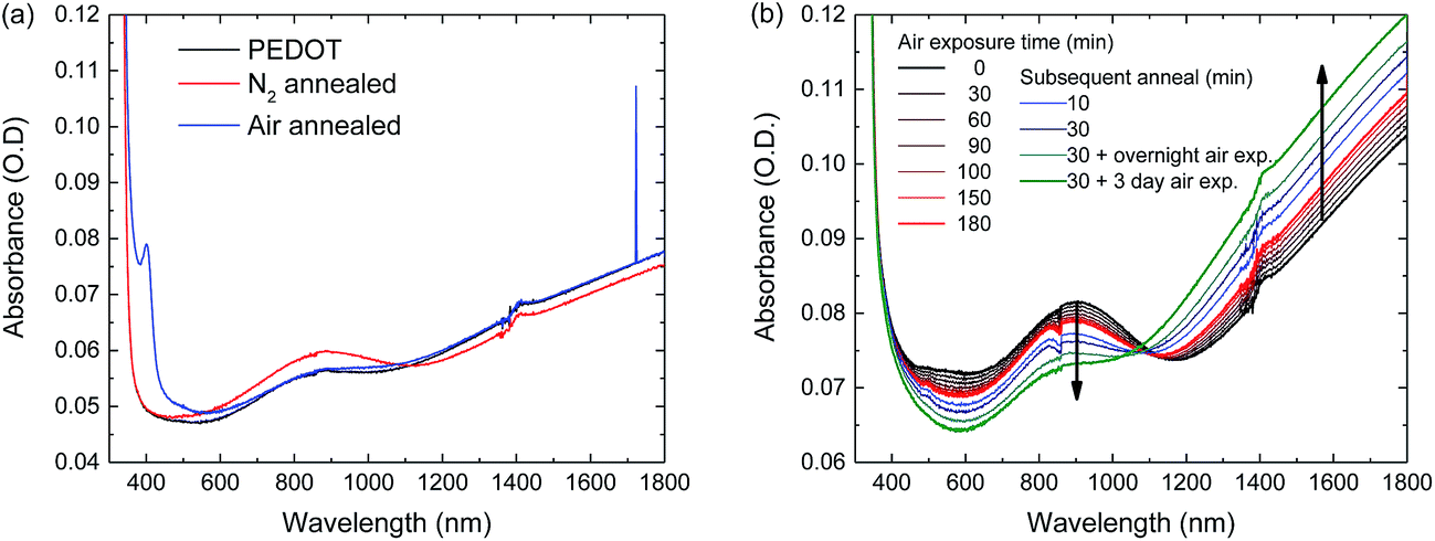
We have shown that oxygen exposure during annealing is required for high performance solar cells and that likely the PEDOT:PSS/perovskite interface deteriorates when the perovskite layer is annealed in N2. It has been reported that PEDOT:PSS can be reduced (electro)chemically by the application of a voltage52 or by exposure to polyethylenimine (PEI)53 and methylamine (MA)54 vapour. In the latter case, the reduced PEDOT:PSS can be re-oxidized by exposure to oxygen.54 To investigate this effect in more detail, PEDOT:PSS layers were spin coated onto glass slides and perovskite layers were hot cast onto the PEDOT:PSS layers in a N2 atmosphere both using the same processing parameters as used for solar cell fabrication. The perovskite layers were then annealed, either in ambient air or in N2 and subsequently the perovskite layers were washed off from the underlying PEDOT:PSS layers using pure DMF. The resulting PEDOT:PSS layers were analysed and compared to fresh PEDOT:PSS layers using UV-vis-NIR spectroscopy (Fig. 7). The spectra show that the polaron absorption at 900 nm of the PEDOT:PSS layer that was underneath the N2-annealed perovskite layer, is higher than that of fresh PEDOT:PSS, and that the bipolaron band at wavelengths ≥1100 nm is lower in intensity (Fig. 7a). These are two clear signatures of chemical de-doping of PEDOT.54 In contrast, the UV-vis-NIR spectrum of the PEDOT:PSS layer that was underneath the air-annealed perovskite layer is very similar to the spectrum of the fresh PEDOT:PSS layer, apart from a narrow peak at 400 nm. The onset and peak position of the 400 nm absorption coincides with the absorbance of orthorhombic lead oxide (PbO)55 and tri-iodide (I3−),56 both of which could be present in the PEDOT:PSS film after deposition and washing off the perovskite layer. The presence of either of the two could however not be confirmed by XPS measurements.
 | ||
| Fig. 7 (a) UV-vis-NIR spectra of a fresh PEDOT:PSS layer and PEDOT:PSS layers on which perovskite layers were deposited, annealed and washed off again. (b) UV-vis-NIR spectra of the PEDOT:PSS layer that was underneath the N2-annealed perovskite layer upon air exposure vs. time. | ||
To confirm that the de-doping of the PEDOT:PSS layer is reversible, the PEDOT:PSS layer that was underneath the N2-annealed perovskite layer was exposed to air. Air exposure of the de-doped PEDOT:PSS layer up to 180 minutes does indeed re-oxidize the PEDOT, evidenced by a reduced polaron absorption at 900 nm and an increased bipolaron absorption above 1100 nm. Annealing of the reduced PEDOT:PSS layer in air speeds up the re-oxidation reaction and prolonged air exposure almost completely re-oxidizes the PEDOT. XPS measurements for sulphur, carbon and oxygen on as cast and washed PEDOT:PSS layers do not show any significant difference in the composition of the material (Fig. S14, ESI†)
Ultraviolet photoelectron spectroscopy (UPS) measurements were performed on air- and N2-annealed perovskite layers and on the PEDOT:PSS layers that were underneath, after washing off the perovskite, to investigate the effect of the reduction and re-oxidation of the PEDOT:PSS layer on the electronic properties of the materials (Fig. 8 and Table 2). By comparing to UPS results for PEDOT:PSS, and PEDOT:PSS that was treated with DMF (Table 2), we see that just casting hot DMF on top of PEDOT:PSS already reduces both the work function (WF, Fermi energy) and ionization potential (IP, valence band energy) of a PEDOT:PSS layer. By subsequent washing with DMF at room temperature, a further decrease can be seen. The striking result is that with spin coating the perovskite precursor on PEDOT:PSS, annealing and washing off of the perovskite layer from the PEDOT:PSS layer, the WF is equal to the IP. The other important observation is that the WF and IP of the PEDOT:PSS layer that was underneath a N2-annealed perovskite film is lower compared to the PEDOT:PSS layer that was underneath an air-annealed perovskite layer. Looking at the results of the perovskite layers deposited on PEDOT:PSS, we see a similar difference with the N2 annealed perovskite layer showing a lower WF than the air annealed one, while the IP of the two perovskite layers remains equal. This suggests that the WF of the perovskite layer is influenced by that of the PEDOT:PSS beneath it. It is worth to note that the difference between the WF of the PEDOT:PSS layer and that of the perovskite layer is similar (∼0.5 eV) for both annealing atmospheres. The difference in the value of the WF of the perovskite layers results in a difference in the built-in voltage of the solar cells, allowing the VOC of the air-annealed perovskite layer to exceed that of the N2-annealed cell. The difference in WF (∼0.12 eV) is comparable to the difference in VOC we measure in J–V sweeps (∼0.07 V). The measured WFs and IPs for fresh PEDOT:PSS and the prepared perovskite layers are similar to previously reported values.57,58
 | ||
| Fig. 8 UPS results of measurements on the top of a perovskite layer deposited onto PEDOT:PSS and annealed in air or nitrogen (a) and a fresh PEDOT:PSS layer and PEDOT:PSS layers that had a N2 or air annealed perovskite layer on top of them that has been washed off (b). | ||
| Layer and processing | Workfunction (eV) | Ionization potential (eV) |
|---|---|---|
| PEDOT:PSS | 4.83 | 5.06 |
| PEDOT:PSS|clean DMF hot cast | 4.48 | 4.83 |
| PEDOT:PSS|clean DMF hot cast|DMF wash | 4.40 | 4.65 |
| PEDOT:PSS|perovskite hot cast|anneal in N2|DMF wash | 4.36 | 4.38 |
| PEDOT:PSS|perovskite hot cast|anneal in air|DMF wash | 4.48 | 4.47 |
| PEDOT:PSS|perovskite hot cast|anneal in N2 | 4.84 | 6.10 |
| PEDOT:PSS|perovskite hot cast|anneal in air | 4.97 | 6.10 |
Conclusions
In this work we have shown that spin coating a perovskite precursor in DMF solution chemically reduces the oxidation state of the PEDOT:PSS hole transport layer on which it is deposited. The partial reduction of PEDOT:PSS from the highly oxidized bipolaron state to the polaron state, reduces the work function of the PEDOT:PSS whereby the work function becomes equal to the ionisation potential. The reduction in the work function of the PEDOT:PSS also reduces the work function of the perovskite layer that is positioned on top of it. Exposure of the reduced PEDOT:PSS to oxygen re-oxidizes the PEDOT:PSS. Even relatively short exposure (8 minutes) of the PEDOT:PSS layer during the annealing of the perovskite layer that is on top of it (partially) restores the oxidation state of the PEDOT and restores its functionality in the solar cell. The bulk properties of the perovskite layer do not seem to change by annealing in different atmospheres. Annealing the perovskite layers in an inert atmosphere therefore produces solar cells of inferior performance, displaying lower VOC and a JSC that is sublinear with light intensity compared to air-annealed devices.Experimental
Device fabrication
Tin doped indium oxide (indium-tin oxide) (ITO) coated and pre-patterned glass substrates (Naranjo substrates) were cleaned by sonication in acetone (Sigma Aldrich), scrubbing in a solution of sodium dodecyl sulfate (SDS, Acros, 99%) in filtered water (Milli-Q), rinsing in deionized water, sonication in 2-propanol (Sigma Aldrich) and 30 minutes of UV-ozone treatment right before use. Poly(3,4-ethylenedioxythiophene)-poly(styrenesulfonate) (PEDOT:PSS, Heraeus Clevios PVP Al 4083) was filtered using a 0.45 μm PVDF filter and spin coated (60 s, 3000 rpm) onto the cleaned substrates.For the hot casting method, the PEDOT:PSS coated substrate was heated for 1 minute at 100 °C right before use, for the cold casting method, the PEDOT:PSS coated substrates were dried at 140 °C for 15 minutes. For the electron transport layer, PCBM (Solenne BV, 99%) was dissolved in a 1:1 (v/v) mixture of chloroform (Biosolve, AR grade) and chlorobenzene (Sigma Aldrich, anhydrous 99.8%) at 20 mg mL−1. The perovskite precursor solution for use with the hot casting method was prepared by weighing 476.9 mg of methylammonium iodide (Dyesol), 303.5 mg of lead(II) acetate trihydrate (Sigma Aldrich, 99.999% trace metal basis) and 55.6 mg of lead(II) chloride (Sigma Aldrich, 98%) in air and adding 1 mL of N,N-dimethylformamide (Sigma Aldrich, anhydrous, 99.8%). The mixture was stirred for 30 minutes at room temperature to completely dissolve all compounds and stirred at 70 °C for 30 minutes before use. The solution was then spin coated onto pre-heated (100 °C) PEDOT:PSS-covered substrates (60 μL, 20 s, 5700 rpm, dynamic) using a specially designed spin coating chuck that minimizes contact between the substrate and the chuck to avoid rapid cooling of the substrate. The perovskite layer was then annealed immediately (100 °C, 8 minutes) and after 1 minute of cooling, coated with PCBM (Solenne BV, 99%) (30 s, 1000 rpm). The device was then transferred into a glovebox, the contact area was cleaned and LiF (1 nm) and Al (100 nm) were thermally evaporated under high vacuum (±3 × 10⁻⁷ mbar) as a back electrode.
The perovskite precursor solution for use with the cold casting method was made by weighing 858.4 mg of methylammonium iodide (Dyesol), 546.3 mg of lead(II) acetate trihydrate (Sigma Aldrich, 99.999% trace metal basis) and 100.1 mg of lead(II) chloride (Sigma Aldrich, 98%) and adding 1 mL of N,N-dimethylformamide (Sigma Aldrich, anhydrous, 99.8%). The mixture was stirred for 30 minutes at room temperature to completely dissolve all the compounds. The solution was then spin coated onto the cleaned, PEDOT:PSS-coated and dried substrates (60 μL, 120 s, 5700 rpm) using the same specially designed spin coating chuck. The perovskite layer was then annealed immediately (100 °C, 15 minutes) and coated with PCBM (Solenne BV, 99%) (30 s, 500 rpm). The device contact area was cleaned and LiF (1 nm) and Al (100 nm) were thermally evaporated under high vacuum (±3 × 10⁻⁷ mbar) as a back electrode.
To accurately control the temperature of the hotplate surfaces of different hotplates, aluminium slabs were used to achieve a homogeneous surface temperature and a surface temperature probe (Testo 0560 1109 mini surface thermometer) was used to measure the temperature. The mentioned temperatures are the temperatures set on the hotplate thermocouple. A set temperature of 100 °C corresponds to a temperature of 94 °C at the top of the aluminium slab measured with the surface probe.
Measurement methods
Layer thicknesses were measured using a Veeco Dektak 150 profilometer.J–V characteristics were measured in a nitrogen environment with a Keithley 2400 source meter under ±100 mW cm−2 white light illumination from a tungsten-halogen lamp filtered by a Schott GG385 UV filter and a Hoya LB120 daylight filter. The cells were masked with a 0.0676 cm2 or 0.1296 cm2 aperture (the physical overlap of the contacts is 0.09 cm2 and 0.16 cm2 respectively) to avoid any underestimation of the active area due to the increased conductivity of the PEDOT:PSS layer by spin coating with DMF. The stabilized J–V measurement protocol used was defined by light soaking at VOC for 5 minutes, followed by a downward sweep (VOC + 0.04 V → −0.04 V) with a step size of 0.02 V. At each voltage the current density was recorded for 10 s and the final value was used for plotting the J–V curve. Fast upwards and downwards J–V sweeps were performed before and after the slow sweep measurement between −0.5 and 1.5 V with a scan speed of 0.25 V s−1.
Short-circuit current densities under AM1.5G conditions were determined by integrating the spectral response with the solar spectrum. Spectral response measurements were conducted under only probe light and 1 sun equivalent operating conditions by using a 530 nm high power LED (Thorlabs M530L3 driven by a DC4104 driver) for bias illumination. The device was kept in a nitrogen filled box behind a quartz window and a circular aperture with a 1 mm radius and irradiated with modulated monochromatic light, from a 50 W tungsten–halogen lamp (Philips focusline) and monochromator (Oriel, Cornerstone 130) with the use of a mechanical chopper (160 Hz). The response was recorded as a voltage from a preamplifier (SR570) using a lock-in amplifier (SR830). A calibrated silicon cell was used as reference (calibrated at the Energy Research Centre of the Netherlands).
Scanning electron microscopy (SEM) was performed on a FEI Quanta 3D FEG.
Low intensity photoluminescence measurements were performed using an Edinburgh Instruments FLSP920 double-monochromator luminescence spectrometer equipped with a multialkali photomultiplier tube and a nitrogen-cooled near IR sensitive photomultiplier (Hamamatsu). The substrate was positioned inside an Oxford Optistat cryostat under a dynamic vacuum. Cryogenic temperatures were achieved by indirectly cooling the substrate. The photoluminescence spectrometer has an internal uncalibrated photodetector to monitor the intensity of excitation beam of which the output is in counts per second. We have used a calibrated Si solar cell to calibrate the reference detector. The light from a xenon light source is monochromated to specific wavelengths for the PL measurements.
High intensity photoluminescence measurements were performed using a 532 nm laser (B&W tek inc. BWN-532-20E/56486) excitation that was chopped using a mechanical chopper (277 Hz). The sample was located in an Oxford Optistat cryostat under dynamic vacuum. The signal was measured using a monochromator (Oriel 77700 at 775 nm) and a Si diode linked to a lock-in amplifier (SR830DSP). The illumination intensity was varied using a double optical density filter wheel (New Focus 5215) and was calibrated at different OD settings using a Si photodiode. The illumination area of the laser beam was determined at different optical densities using a Gentec Beamage 3.0 beam diagnostic tool (1/e2 value was used).
Electroluminescence measurements were performed in a nitrogen environment using a reference Si cell and two Keithley 2400 source meters to control the voltage and record the current flowing through the test cell and record the current flow out of the Si reference cell. Dividing the two current flows results in a crude electroluminescence external quantum efficiency value that is not absolute but can be used to compare samples measured in the same setup.
UPS measurements were performed in a multi-chamber ESCALAB II system using 6 V bias and the HeI line at 21.22 eV. The Fermi level reference was established on an in situ sputter-cleaned Au film. The ionization potential and the work function are derived from the energy difference between the secondary electron edge and, respectively, the valence band edge or the position of the Fermi energy. Samples were transferred from gloveboxes to the measurement equipment completely in an N2 atmosphere to avoid any effects of oxygen exposure. XPS measurements were performed with the same instrument using Mg (Kα) radiation.
V OC vs. light intensity measurements were performed using a Keithley 2400 source meter and 405 and 730 nm high power LEDs (Thorlabs M405L3 and M730L4 driven by a DC4104 driver) for illumination.
Conflicts of interest
There are no conflicts to declare.Acknowledgements
The research received funding from the European Research Council under the European Union's Seventh Framework Programme (FP/2007-2013)/ERC Grant Agreement No. 339031, forms part of the Solliance programme, and has received funding from the Ministry of Education, Culture and Science (Gravity program 024.001.035).References
- A. Kojima, K. Teshima, Y. Shirai and T. Miyasaka, J. Am. Chem. Soc., 2009, 131, 6050–6051 CrossRef CAS PubMed.
- H.-S. Kim, C.-R. Lee, J.-H. Im, K.-B. Lee, T. Moehl, A. Marchioro, S.-J. Moon, R. Humphry-Baker, J.-H. Yum, J. E. Moser, M. Grätzel and N.-G. Park, Sci. Rep., 2012, 2, 591 CrossRef PubMed.
- M. M. Lee, J. Teuscher, T. Miyasaka, T. N. Murakami and H. J. Snaith, Science, 2012, 338, 643–648 CrossRef CAS PubMed.
- M. Saliba, T. Matsui, J.-Y. Seo, K. Domanski, J.-P. Correa-Baena, M. K. Nazeeruddin, S. M. Zakeeruddin, W. Tress, A. Abate, A. Hagfeldt and M. Grätzel, Energy Environ. Sci., 2016, 9, 1989–1997 CAS.
- W. S. Yang, B.-W. Park, E. H. Jung, N. J. Jeon, Y. C. Kim, D. U. Lee, S. S. Shin, J. Seo, E. K. Kim, J. H. Noh and S. Il Seok, Science, 2017, 356, 1376–1379 CrossRef CAS PubMed.
- V. D'Innocenzo, G. Grancini, M. J. P. Alcocer, A. R. S. Kandada, S. D. Stranks, M. M. Lee, G. Lanzani, H. J. Snaith and A. Petrozza, Nat. Commun., 2014, 5, 3586 Search PubMed.
- L. M. Pazos-Outón, M. Szumilo, R. Lamboll, J. M. Richter, M. Crespo-Quesada, M. Abdi-Jalebi, H. J. Beeson, M. Vrućinić, M. Alsari, H. J. Snaith, B. Ehrler, R. H. Friend and F. Deschler, Science, 2016, 351, 1430–1433 CrossRef PubMed.
- C.-S. Jiang, M. Yang, Y. Zhou, B. To, S. U. Nanayakkara, J. M. Luther, W. Zhou, J. J. Berry, J. Van De Lagemaat, N. P. Padture, K. Zhu and M. M. Al-jassim, Nat. Commun., 2015, 6, 8397 CrossRef CAS PubMed.
- C. Wehrenfennig, G. E. Eperon, M. B. Johnston, H. J. Snaith and L. M. Herz, Adv. Mater., 2014, 26, 1584–1589 CrossRef CAS PubMed.
- T. M. Schmidt, T. T. Larsen-Olsen, J. E. Carlé, D. Angmo and F. C. Krebs, Adv. Energy Mater., 2015, 5, 1500569 CrossRef.
- K. Hwang, Y.-S. Jung, Y.-J. Heo, F. H. Scholes, S. E. Watkins, J. Subbiah, D. J. Jones, D.-Y. Kim and D. Vak, Adv. Mater., 2015, 27, 1241–1247 CrossRef CAS PubMed.
- Y. Galagan, E. W. C. Coenen, W. J. H. Verhees and R. Andriessen, J. Mater. Chem. A, 2016, 4, 5700–5705 CAS.
- G. E. Eperon, S. D. Stranks, C. Menelaou, M. B. Johnston, L. M. Herz and H. J. Snaith, Energy Environ. Sci., 2014, 7, 982–988 CAS.
- G. E. Eperon, G. M. Paternò, R. J. Sutton, A. Zampetti, A. A. Haghighirad, F. Cacialli and H. J. Snaith, J. Mater. Chem. A, 2015, 3, 19688–19695 CAS.
- W. Liao, D. Zhao, Y. Yu, N. Shrestha, K. Ghimire, C. R. Grice, C. Wang, Y. Xiao, A. J. Cimaroli, R. J. Ellingson, N. J. Podraza, K. Zhu, R. G. Xiong and Y. Yan, J. Am. Chem. Soc., 2016, 138, 12360–12363 CrossRef CAS PubMed.
- J. H. Heo, D. H. Song, H. J. Han, S. Y. Kim, J. H. Kim, D. Kim, H. W. Shin, T. K. Ahn, C. Wolf, T. W. Lee and S. H. Im, Adv. Mater., 2015, 27, 3424–3430 CrossRef CAS PubMed.
- C.-C. Chueh, C.-Y. Liao, F. Zuo, S. T. Williams, P.-W. Liang and A. K.-Y. Jen, J. Mater. Chem. A, 2015, 3, 9058–9062 CAS.
- W. Zhang, M. Saliba, D. T. Moore, S. K. Pathak, M. T. Hörantner, T. Stergiopoulos, S. D. Stranks, G. E. Eperon, J. A. Alexander-Webber, A. Abate, A. Sadhanala, S. Yao, Y. Chen, R. H. Friend, L. A. Estroff, U. Wiesner and H. J. Snaith, Nat. Commun., 2015, 6, 6142 CrossRef CAS PubMed.
- K. L. Gardner, J. G. Tait, T. Merckx, W. Qiu, U. W. Paetzold, L. Kootstra, M. Jaysankar, R. Gehlhaar, D. Cheyns, P. Heremans and J. Poortmans, Adv. Energy Mater., 2016, 6, 1600386 CrossRef.
- K. H. Hendriks, J. J. van Franeker, B. J. Bruijnaers, J. A. Anta, M. M. Wienk and R. A. J. Janssen, J. Mater. Chem. A, 2017, 5, 2346 CAS.
- S. Bae, S. J. Han, T. J. Shin and W. H. Jo, J. Mater. Chem. A, 2015, 3, 23964–23972 CAS.
- N. Ahn, D.-Y. Son, I.-H. Jang, S. M. Kang, M. Choi and N.-G. Park, J. Am. Chem. Soc., 2015, 137, 8696–8699 CrossRef CAS PubMed.
- N. K. Noel, S. N. Habisreutinger, B. Wenger, M. T. Klug, M. T. Hörantner, M. B. Johnston, R. J. Nicholas, D. T. Moore and H. J. Snaith, Energy Environ. Sci., 2017, 10, 145–152 CAS.
- F. K. Aldibaja, L. Badia, E. Mas-Marzá, R. S. Sánchez, E. M. Barea and I. Mora-Sero, J. Mater. Chem. A, 2015, 3, 9194–9200 CAS.
- G. Li, T. Zhang and Y. Zhao, J. Mater. Chem. A, 2015, 3, 19674–19678 CAS.
- W. Qiu, T. Merckx, M. Jaysankar, C. Masse de la Huerta, L. Rakocevic, W. Zhang, U. W. Paetzold, R. Gehlhaar, L. Froyen, J. Poortmans, D. Cheyns, H. J. Snaith and P. Heremans, Energy Environ. Sci., 2016, 9, 484–489 CAS.
- J. Qing, H.-T. Chandran, Y.-H. Cheng, X.-K. Liu, H.-W. Li, S.-W. Tsang, M.-F. Lo and C.-S. Lee, ACS Appl. Mater. Interfaces, 2015, 7, 23110–23116 CAS.
- Z. Zhang, D. Wei, B. Xie, X. Yue, M. Li, D. Song and Y. Li, Sol. Energy, 2015, 122, 97–103 CrossRef CAS.
- B. Conings, A. Babayigit, M. T. Klug, S. Bai, N. Gauquelin, N. Sakai, J. T.-W. Wang, J. Verbeeck, H.-G. Boyen and H. J. Snaith, Adv. Mater., 2016, 28, 10701–10709 CrossRef CAS PubMed.
- N. J. Jeon, J. H. Noh, Y. C. Kim, W. S. Yang, S. Ryu and S. Il Seok, Nat. Mater., 2014, 13, 897–903 CrossRef CAS PubMed.
- J. Xiong, B. Yang, R. Wu, C. Caoa, Y. Huanga, C. Liu, Z. Hu, H. Huang, Y. Gao and J. Yang, Org. Electron., 2015, 24, 106–112 CrossRef CAS.
- M. Liu, M. B. Johnston and H. J. Snaith, Nature, 2013, 501, 395–398 CrossRef CAS PubMed.
- L. K. Ono, M. R. Leyden, S. Wang and Y. Qi, J. Mater. Chem. A, 2016, 4, 6693–6713 CAS.
- Q. Chen, H. Zhou, Z. Hong, S. Luo, H.-S. Duan, H.-H. Wang, Y. Liu, G. Li and Y. Yang, J. Am. Chem. Soc., 2014, 136, 622–625 CrossRef CAS PubMed.
- C. Wehrenfennig, M. Liu, H. J. Snaith, M. B. Johnston and L. M. Herz, Energy Environ. Sci., 2014, 7, 2269 CAS.
- M. M. Tavakoli, L. Gu, Y. Gao, C. Reckmeier, J. He, A. L. Rogach, Y. Yao and Z. Fan, Sci. Rep., 2015, 5, 14083 CrossRef PubMed.
- M. Saliba, K. W. Tan, H. Sai, D. T. Moore, T. Scott, W. Zhang, L. A. Estro, U. Wiesner and H. J. Snaith, J. Phys. Chem. C, 2014, 118, 17171–17177 CAS.
- Y. Chen, Y. Zhao and Z. Liang, Chem. Mater., 2015, 27, 1448–1451 CrossRef CAS.
- S. R. Raga, M.-C. Jung, M. V. Lee, M. R. Leyden, Y. Kato and Y. Qi, Chem. Mater., 2015, 27, 1597–1603 CrossRef CAS.
- A. Dualeh, N. Tétreault, T. Moehl, P. Gao, M. K. Nazeeruddin and M. Grätzel, Adv. Funct. Mater., 2014, 24, 3250–3258 CrossRef CAS.
- Z. Xiao, Q. Dong, C. Bi, Y. Shao, Y. Yuan and J. Huang, Adv. Mater., 2014, 26, 6503–6509 CrossRef CAS PubMed.
- J. J. van Franeker, K. H. Hendriks, B. J. Bruijnaers, M. W. G. M. Verhoeven, M. M. Wienk and R. A. J. Janssen, Adv. Energy Mater., 2017, 7, 1601822 CrossRef.
- G. E. Eperon, S. N. Habisreutinger, T. Leijtens, B. J. Bruijnaers, J. J. van Franeker, D. W. deQuilettes, S. Pathak, R. J. Sutton, G. Grancini, D. S. Ginger, R. A. J. Janssen, A. Petrozza and H. J. Snaith, ACS Nano, 2015, 9, 9380–9393 CrossRef CAS PubMed.
- C.-G. Wu, C.-H. Chiang, Z.-L. Tseng, M. K. Nazeeruddin, A. Hagfeldt and M. Grätzel, Energy Environ. Sci., 2015, 8, 2725–2733 CAS.
- S. Pathak, A. Sepe, A. Sadhanala, F. Deschler, A. Haghighirad, N. Sakai, K. C. Goedel, S. D. Stranks, N. Noel, M. Price, S. Hüttner, N. A. Hawkins, R. H. Friend, U. Steiner and H. J. Snaith, ACS Nano, 2015, 9, 2311–2320 CrossRef CAS PubMed.
- L. J. A. Koster, V. D. Mihailetchi, R. Ramaker and P. W. M. Blom, Appl. Phys. Lett., 2005, 86, 1–3 CrossRef.
- S. R. Cowan, A. Roy and A. J. Heeger, Phys. Rev. B: Condens. Matter Mater. Phys., 2010, 82, 245207 CrossRef.
- K. Tvingstedt, L. Gil-Escrig, C. Momblona, P. Rieder, D. Kiermasch, M. Sessolo, A. Baumann, H. J. Bolink and V. Dyakonov, ACS Energy Lett., 2017, 2, 424–430 CrossRef CAS.
- K. Tvingstedt and C. Deibel, Adv. Energy Mater., 2016, 6, 1502230 CrossRef.
- O. Malinkiewicz, A. Yella, Y. H. Lee, G. M. Espallargas, M. Graetzel, M. K. Nazeeruddin and H. J. Bolink, Nat. Photonics, 2014, 8, 128–132 CrossRef CAS.
- O. Bubnova, Z. U. Khan, H. Wang, S. Braun, D. R. Evans, M. Fabretto, P. Hojati-Talemi, D. Dagnelund, J.-B. Arlin, Y. H. Geerts, S. Desbief, D. W. Breiby, J. W. Andreasen, R. Lazzaroni, W. M. Chen, I. Zozoulenko, M. Fahlman, P. J. Murphy, M. Berggren and X. Crispin, Nat. Mater., 2013, 13, 190–194 CrossRef PubMed.
- P. M. Beaujuge and J. R. Reynolds, Chem. Rev., 2010, 110, 268–320 CrossRef CAS PubMed.
- S. Fabiano, S. Braun, X. Liu, E. Weverberghs, P. Gerbaux, M. Fahlman, M. Berggren and X. Crispin, Adv. Mater., 2014, 26, 6000–6006 CrossRef CAS PubMed.
- T. Liu, F. Jiang, J. Tong, F. Qin, W. Meng, Y. Jiang, Z. Li and Y. Zhou, J. Mater. Chem. A, 2016, 4, 4305–4311 CAS.
- R. C. Keezer, D. L. Bowman and J. H. Becker, J. Appl. Phys., 1968, 39, 2062–2066 CrossRef CAS.
- N. Li, L. Shi, X. Wang, F. Guo and C. Yan, Int. J. Anal. Chem., 2011, 130102 Search PubMed.
- P. Schulz, E. Edri, S. Kirmayer, G. Hodes, D. Cahen and A. Kahn, Energy Environ. Sci., 2014, 7, 1377 CAS.
- S. Olthof and K. Meerholz, Sci. Rep., 2017, 7, 40267 CrossRef CAS PubMed.
Footnote |
| † Electronic supplementary information (ESI) available. See DOI: 10.1039/c7ta11128b |
| This journal is © The Royal Society of Chemistry 2018 |