Microstructure and doping effect on the enhancement of the thermoelectric properties of Ni doped Dy filled CoSb3 skutterudites
Received
1st August 2018
, Accepted 18th September 2018
First published on 18th September 2018
Abstract
The thermoelectric properties of nanostructured Ni doped Dy filled CoSb3 skutterudites (Dy0.4Co4−xNixSb12 (x = 0, 0.4, and 0.8)) have been reported. The samples are processed using a solid-state synthesis route. The structural analysis of the samples using X-ray diffraction reveals the existence of a single skutterudite phase in Ni doped samples irrespective of the Ni concentration. Microstructure studies using transmission electron microscopy and scanning electron microscopy show the existence of nanometer (∼60 nm) size equiaxed grains in the investigated samples. A few recrystallized elongated grains (∼200 nm) are observed in the Dy0.4Co3.2Ni0.8Sb12 sample. The power factor of the Dy0.4Co3.2Ni0.8Sb12 sample is enhanced to 5.2 mW mK−2, which is the highest power factor for the doped ternary skutterudites reported so far. The enhancement of the power factor is due to the substantial reduction in electrical resistivity with an increase in Ni concentration at higher temperature. The lattice thermal conductivity is drastically reduced to 0.3 W mK−1 at 773 K in the Dy0.4Co3.2Ni0.8Sb12 sample due to the enhanced phonon scattering from Ni induced point defects and grain boundaries. As a result, a huge increase in the figure of merit (ZT ∼ 1.4 ± 0.14) at 773 K is observed in the Dy0.4Co3.2Ni0.8Sb12 sample, the highest among those of the single element filled CoSb3 skutterudites reported so far at this temperature. Hence, Ni doping could enhance the thermoelectric efficiency of Dy filled CoSb3 skutterudites. This can be taken as a reference to synthesize CoSb3 skutterudite thermoelectric materials having a higher figure of merit.
1 Introduction
Over the past few years, efforts have been made to enhance the thermoelectric properties of several material systems including half-Heuslers,1–4 skutterudites,5–8 silicides,9,10 tellurides11–14 and Zintl phases.15 Among the potential thermoelectric (TE) materials, CoSb3-based skutterudite materials were highlighted as efficient TE materials for waste heat recovery in intermediate temperature range applications.4–7 The performance of TE materials depends on their figure of merit (ZT), which is given by the relation ZT = S2T/ρκ, where S, ρ and κ are the thermopower, electrical resistivity and thermal conductivity at absolute temperature T, respectively.5 To exhibit enhanced TE properties, the materials must have a higher power factor (S2/ρ) and low κ. However it is difficult to simultaneously enhance the power factor and decrease the thermal conductivity because the two properties are correlated with each other. Various reports have been published on the phonon-glass-electron-crystal (PGEC) behavior of TE materials to attain higher TE efficiency.16,17 The PGEC concept proposed by Slack was found to be the most important idea guiding contemporary TE research.17 Slack suggested that semiconducting crystals containing one or more atoms/molecules that are dynamically disordered in an otherwise ordered structure should have very low lattice thermal conductivity and potentially enhanced TE performance.17–19 Presumably, localized vibrations associated with the disordered constituents would be effective in scattering the heat carrying phonons, perhaps without significant detriment to the electrical transport properties.16 This insightful guiding principle has resulted in the discovery of new classes of high-performance TE materials, such as filled skutterudites18,19 and intermetallic clathrates,20,21 which are characterized by cage-like crystal structures that encapsulate the so-called “rattling” guest atoms.22 It is known that skutterudite TE materials consist of a framework of vertex-linked CoSb6 octahedra, with a unit cell containing Co cubelets and planar four-membered Sb4 rings located at the body-centre position of six of them. The remaining two bcc positions are the cages to be filled by the rattling atoms. The vibrations of the guest fillers lead to strong scattering of phonons, producing a significant reduction in lattice thermal conductivity.18,23,24 If multiple fillers are introduced into the cavity (i.e., multiply filled skutterudites), it will result in vibrations of different resonance frequencies and this promotes scattering over a broader range of the phonon spectrum with a higher reduction in lattice thermal conductivity.5,6 But the multiple filling may make the TE material system more complex and non-reproducible for practical applications. In addition, the availability of RE elements is scarce nowadays. Another strategy to enhance the TE properties is to reduce the particle size of the materials by nanostructuring and nanoprecipitation, which can reduce the lattice thermal conductivity of the skutterudite by increasing the phonon scattering at the grain boundaries or interfaces.25–27 An alternative approach is the introduction of enhanced point defect scattering through doping with suitable elements (for instance, replacement of Co by Fe and Ni, and replacement of Sb by Te, Se, As, etc.), which also leads to a reduction of lattice thermal conductivity.28,29 In the mean time, charge carriers donated by the dopants to the Fermi level help in decreasing ρ and hence the power factor increases.
In our work, Dy is chosen as a RE atom because it is heavier than other RE atoms like Sm and Nd/Pr. Rogl et al.5 reported that by filling n-type CoSb3 skutterudites with multiple RE atoms (Sm, La, Ce, Pr and Nd), their figure of merit was enhanced to 1.6 at 825 K. Our target is to fill the cage of the skutterudite with a single element and hence Dy is chosen as a filler. Ni is chosen as a dopant to replace the Co atom as Ni could enhance the electrical properties of skutterudites as reported earlier by various authors.30–41 Also Ni helps in improving the mechanical properties of alloys.42 Moreover, replacement of Co by Ni is very cost-effective and hence can be viable for commercial large-scale production of these materials.43 Therefore to understand the effect of Ni doping on the microstructure and TE properties of skutterudites, in our work, we synthesized Ni doped CoSb3 skutterudites (Dy0.4C4−xNixSb12, x = 0.4 and 0.8) partially filled with Dy using a ball milling and spark plasma sintering route. Recrystallized elongated grains are observed in the case of the Dy0.4Co3.2Ni0.8Sb12 sample. There is a drastic enhancement of TE properties in the Dy0.4Co3.2Ni0.8Sb12 sample due to simultaneous reduction of electrical resistivity and lattice thermal conductivity. The detailed microstructure, and TE and mechanical properties of the investigated samples have been reported.
2 Experimental
We synthesized polycrystalline Ni doped Dy filled CoSb3 skutterudite samples (Dy0.4Co4Sb12, Dy0.4Co3.6Ni0.4Sb12 and Dy0.4Co3.2Ni0.8Sb12) by a solid state reaction route using a ball milling and spark plasma sintering (SPS) route as discussed elsewhere.7 The constituent elements Co (99.8%), Sb (99.8% purity), Dy (99.9%) and Ni (99.8%) were taken in the form of powders. The powders were mechanically alloyed in a Retsch Ball Mill for 10 h under an Ar atmosphere using a WC-Co grinding medium. The milled powders were pelletized using a Dr Sinter Spark Plasma Sintering Unit (Model SPS-625, SPS Syntex Inc., Japan) at 873 K and 50 MPa pressure. The SPS pellets are 15 mm in diameter and 4 mm in thickness. Two pellets of each sample were consolidated using SPS in order to carry out the electrical resistivity, thermopower and thermal conductivity measurements from the same batch of ball-milled powders.
The structural investigations were carried out using a Rigaku X-ray diffractometer. The grain morphology and microstructure of the SPS pellets were investigated using TECNAI T20 Transmission Electron Microscopy (TEM) and ZEISS Merlin Scanning Electron Microscopy (SEM). For the TEM specimen, circular discs of 3 mm diameter were cut from the SPS pellets and polished. The polished discs were dimple ground using a Gatan Dimple grinder followed by ion milling using a precision ion polishing system (PIPS, M/S Gatan Inc, UA).
Two-dimensional scanning of thermopower (S) measurements was carried out on the investigated samples using a Potential Seebeck Microprobe (PSM-II) instrument supplied by M/S Panco, Germany. The instrument has a copper tip, which scans the sample with a step size of 10 μm in X- and Y-directions. This technique provides information regarding the local distribution of the thermopower with a spatial resolution of 2 μm. Variation of electrical resistivity (ρ) and thermopower (S) with temperature was measured using a Seebsys apparatus (M/S Norecs, Norway). A NETZSCH LFA instrument was used to measure the thermal diffusivity of the samples in a temperature range of 300 K to 773 K using the laser-flash technique. A thin graphite layer was coated on the pellets to maximize full absorption at the front surface and the highest emissivity from the backside. The thermal conductivity (κ) is determined using the equation κ = thermal diffusivity × specific heat × density. Differential Scanning Calorimetry (DSC-SETARAM Labsys) was employed to measure the specific heat capacity (Cp). All the measurements of TE properties were performed from 300 K to 773 K. The uncertainty in electrical resistivity and thermal conductivity measurements is ±5 and ±5% respectively. The electronic carrier concentration (n) at 300 K was determined using an in-house Hall measurement set-up. The dc current was fixed at 50 mA and a variable magnetic field 0–0.5 T was used for the measurements. The dimension of the sample for Hall measurement was 1.5 mm × 2 mm × 8 mm. The ‘n’ value was evaluated using the equation “n = 1/(eRH)”, where RH and e are the Hall coefficient and electronic charge respectively. The carrier motility ‘μ’ of all samples was estimated using the expression μ = RH/ρ. Mechanical testing at 300 K and 773 K was carried out using a tensile testing machine (Zwick/Roell Z100). For the measurements, the cuboidal sample of 2 mm × 2 mm × 3 mm was cut from SPS pellets using a precision diamond cutter.
3 Results and discussion
3.1 Phase formation and microstructure evolution
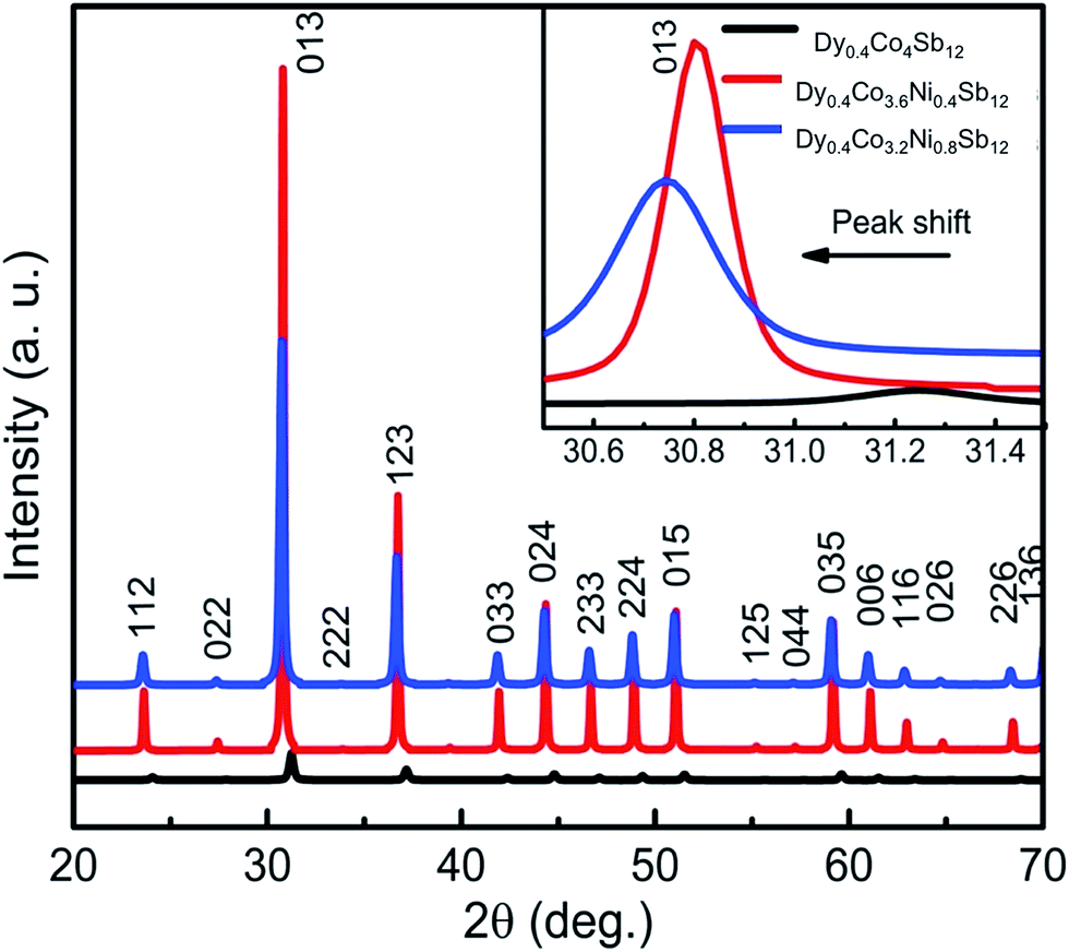
X-ray diffraction patterns collected from the SPS samples are presented in Fig. 1. Fig. 1 shows that after SPS, Dy0.4Co3.6Ni0.4Sb12 and Dy0.4Co3.2Ni0.8Sb12 samples are completely pure skutterudite phases. The Bragg peak appearing at 2θ = 31.26 degree is the most intense peak from the (013) plane of the CoSb3 phase (X-pert reference code: 98-007-6888) and shifts towards left with an increase in Ni concentration indicating the increase in lattice parameters with increasing Ni. The lattice parameter is evaluated using Rietveld refinement of the XRD data and is presented in Table 1. The increase in the lattice parameter with an increase in Ni doping concentration is due to the gradual merging of the secondary Sb phase into the lattice. The crystallite size calculated from the XRD data using full width half maxima of the most intense peak from the (013) plane confirms that the investigated samples are of nanocrystalline nature (Table 1). The nanocrystalline nature of skutterudites is also reported earlier by several authors.42–44 The density of all the samples was calculated using the Archimedes principle and is tabulated in Table 1. It shows that the investigated samples are of high density, and the relative density is ∼98% and above.
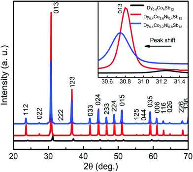 |
| | Fig. 1 X-ray diffraction pattern from the spark plasma sintered pellets of Dy0.4Co4Sb12, Dy0.4Co3.6Ni0.4Sb12 and Dy0.4Co3.2Ni0.8Sb12 samples. | |
Table 1 Physical parameters calculated for all the samples from XRD, TEM and thermoelectric data
| Sample |
Dy0.4Co4Sb12 |
Dy0.4Co3.6Ni0.4Sb12 |
Dy0.4Co3.2Ni0.8Sb12 |
| Nominal composition |
2.44:24.4:73.16 |
2.44:21.96:2.44:73.16 |
2.44:19.52:4.88:73.16 |
| Actual composition |
2.66:26.33:71.01 |
2.87:24.43:2.4:70.3 |
3.3:22.17:4.93:69.6 |
| Lattice parameter (Å) |
9.022 |
9.036 |
9.039 |
| Crystallite size (nm) |
31 |
56 |
36 |
| Grain size (nm) |
60 |
60 |
60/200 |
| Density (g cm−3) |
7.8 |
7.8 |
7.8 |
| Density (% theoretical density) |
98 |
98.4 |
98.5 |
|
ρ at 300 K (10−6 Ω.m) |
385 |
20.6 |
7.4 |
|
S At 300 K (μV K−1) |
−75 |
−100 |
−90 |
|
n (1020 cm−3, calculated from Seebeck data) |
1.3 |
6.1 |
6.3 |
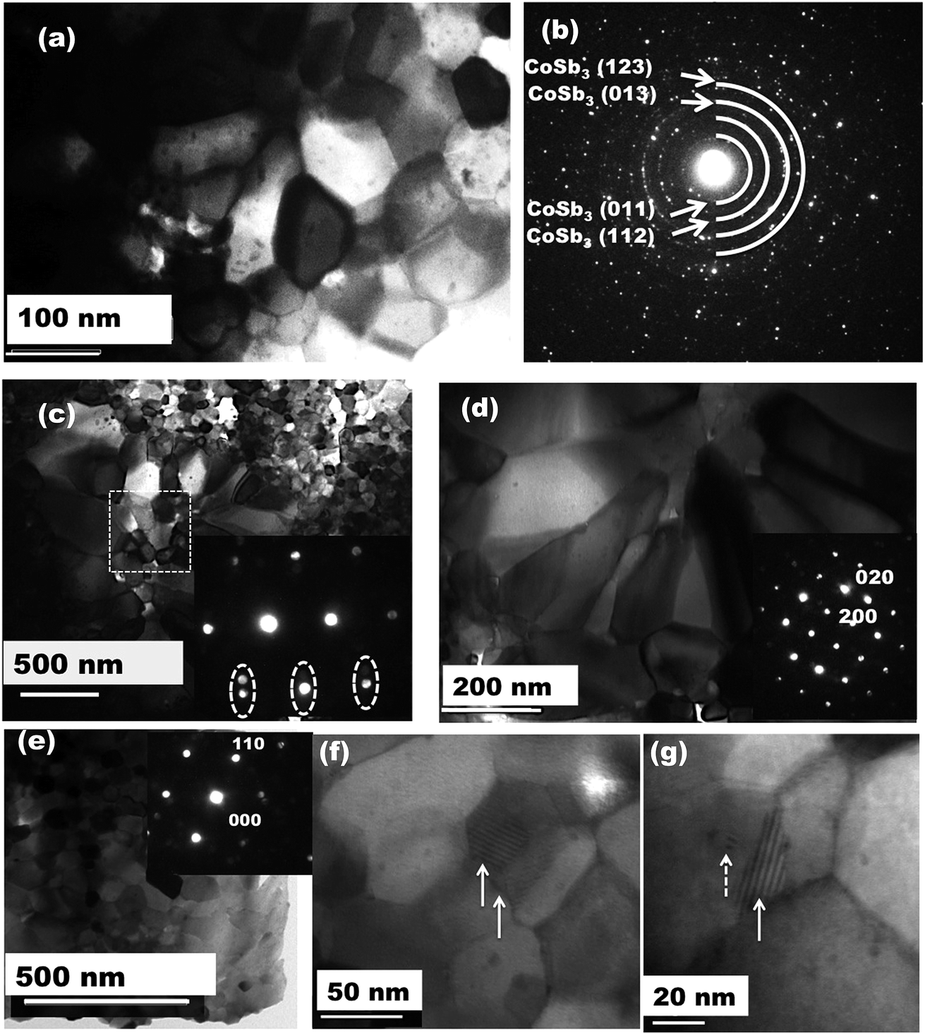
In order to understand the detailed microstructure evolution in the investigated samples, high resolution TEM has been carried out. Fig. 2 shows the typical bright field TEM images and selected area electron diffraction (SAED) from Dy0.4Co3.6Ni0.4Sb12 and Dy0.4Co3.2Ni0.8Sb12 samples. In the case of the Dy0.4Co4Sb12 sample, it is clearly seen that well-developed angular grains with an average size of 60 nm are obtained. The grain size is in agreement with that of the pure CoSb3 fabricated by the solid state method (>100 nm),45,46 but much smaller than those of the samples fabricated by arc melting (∼5 μm).47 The nanometer size grains in our investigated samples might help in improving the phonon scattering.48–50Fig. 2(b and c) show the SAED pattern from the Dy0.4Co4Sb12 and the diffraction ring corresponds to the CoSb3 phase. Fig. 2(c) shows the bright field TEM images of the Dy0.4Co3.2Ni0.8Sb12 sample. The grain morphology and distribution are completely different from those of the other two samples. It is really surprising to see that there is a bimodal distribution of grains, where smaller grains have a size of < 100 nm (∼60 nm) and bigger elongated grains have an average size around 200 nm in the Dy0.4Co3.2Ni0.8Sb12 sample. This type of bimodal distribution of grains is not reported earlier for Ni doped skutterudites.41,42,44Fig. 2(d) shows bigger grains of size ∼200 nm and the inset shows the diffraction pattern from the [220] plane of CoSb3. Fig. 2(e) shows smaller grains of size ∼60 nm and the inset shows the SAED pattern corresponding to the [111] plane for cubic CoSb3. No secondary phase is observed in the Dy0.4Co3.2Ni0.8Sb12 sample. The larger grains in the Dy0.1Ni0.2Co0.8Sb3 sample can be referred to as recrystallized grains. Since the ball milled powder of the Dy0.4Co3.2Ni0.8Sb12 sample contains more skutterudite phase, the phase evolution completed in a very short span of time during SPS. Once the phase formation is complete, grain growth/recrystallization might happen as the dwelling temperature of SPS is 873 K which is more than 0.5 times the melting point of the CoSb3 phase (1147 K).51 Although, all the samples are processed under the same conditions, only the Dy0.4Co3.2Ni0.8Sb12 sample contains bimodal grains and the other two samples have only equiaxed grains. The inset in Fig. 2(c) shows the SAED pattern from the marked dotted square area of Fig. 2(c). It is very clearly observed that there exist two cubic CoSb3 lattices close to each other having different angles or slightly tilted to each other, which is indicated by the two close diffraction spots (marked in dotted circles). From Fig. 2(c–e), we can confirm that the Dy0.1Co0.8Ni0.2Sb3 sample contains nano to submicron size grains. Several moire fringes are observed in the high resolution TEM bright field images of the Dy0.1Co0.8Ni0.2Sb3 sample as indicated by solid arrow lines in Fig. 2(f and g). More fringes arise because of overlapping lattice fringes from adjacent crystals with slight misorientation. A few defects are also observed on the grains as indicated by the dotted arrow line in Fig. 2(g).
 |
| | Fig. 2 (a) Typical TEM bright field image of the Dy0.4Co4Sb12 sample showing the distribution of grains, (b) SAED pattern from the Dy0.4Co4Sb12 sample, (c) typical TEM bright field image of Dy0.1Co0.8Ni0.2Sb3 showing the bimodal distribution of grains, the inset in (c) shows the diffraction pattern from the [111] axis pattern of cubic CoSb3, (d) bright field image of large grains in the Dy0.4Co3.2Ni0.8Sb12 sample and the corresponding SAED pattern, (e) small grains and the corresponding SAED pattern of Dy0.4Co3.2Ni0.8Sb12, (f) and (g) HRTEM of the grains showing the moire fringes (indicated by solid arrow) and defects in the grains (indicated by the dotted arrow). | |
SEM and EDX have been carried out on the investigated samples to know the overall microstructure of the investigated samples. The secondary images collected from Dy0.4Co4Sb12, Dy0.4Co3.6Ni0.4Sb12 and Dy0.4Co3.2Ni0.8Sb12 samples are presented in Fig. 3(a–d). It shows that in the case of Dy0.4Co4Sb12 and Dy0.4Co3.6Ni0.4Sb12 samples, nanometer size grains are distributed throughout the sample. But in the case of the Dy0.4Co3.2Ni0.8Sb12 sample, the bimodal distribution of grains is clearly visible. The Dy0.4Co3.2Ni0.8Sb12 sample has nanometer sized grains like the other two investigated samples whereas there is evolution of elongated dendritic grains at certain places. The back-scattered image (Fig. 3(d)) shows that the dendritic grains are of single phase and there is no secondary phase present on the large dendritic grains. The appearance of dendritic grains may be due to the secondary recrystallization of the grains. During secondary recrystallization, the grain size changes radically and hence very large grains are present along with small grains. The appearance of dendritic grain growth is generally observed in Ni based superalloys.51 This means that in the case of the Dy0.4Co3.2Ni0.8Sb12 sample, since the Ni concentration is higher, it promotes the secondary recrystallization due to the effect of triggering the strain induced migration of grain boundaries.51 The triggering happens due to the fact that SPS is carried out at 873 K for 30 min, which is more than 0.5 times the melting point of the CoSb3 skutterudite phase (1147 K). Hence it can be concluded that with an increase in Ni concentration in CoSb3 skutterudites, dendritic grain growth might happen in the samples prepared by a solid-state synthesis route. To know the actual composition of the individual elements present in the samples, EDX has been carried out over a large area (5 μm × 5 μm) and the average value is given in Table 1. It can be easily noticed that the actual composition is slightly different from the nominal composition of the samples. The nominal compositions taken for Dy0.4Co4Sb12, Dy0.4Co3.6Ni0.4Sb12 and Dy0.4Co3.2Ni0.8Sb12 samples are 2.44:24.4:73.16, 2.44:21.96:2.44:73.16 and 2.44:19.52:4.88:73.16 respectively, whereas, the actual compositions calculated from EDX data for Dy0.4Co4Sb12, Dy0.4Co3.6Ni0.4Sb12 and Dy0.4Co3.2Ni0.8Sb12 samples are 2.66:26.33:71.01, 2.87:24.43:2.4:70.3 and 3.3:22.17:4.93:69.6 respectively. There is 3 to 5% loss of Sb with an increase in Ni concentration. It was reported earlier that the Sb vacancy in CoSb3 reduces the lattice thermal conductivity, which will be discussed later.52
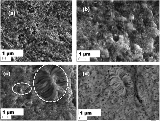 |
| | Fig. 3 SEM image at the fracture surface of (a) Dy0.4Co4Sb12, (b) Dy0.4Co3.6Ni0.4Sb12 and (c) Dy0.4Co3.2Ni0.8Sb12 samples. (d) shows the backscattered image from the Dy0.4Co3.2Ni0.8Sb12 sample. The dotted circles in (c) show larger grains present in the Dy0.4Co3.2Ni0.8Sb12 sample. | |
3.2 PSM analysis
Fig. 4 shows the PSM data analysis of the investigated samples. The variation of room temperature thermopower (S) is different in all the samples. The S value is negative in all the investigated samples indicating the electrons as the dominant charge carriers in the samples. In the case of the Dy0.4Co4Sb12 sample, there is broad variation of S values. S varies from −83 to −127 μV K−1 and the average value is ∼ −100 μV K−1. The S value of −127 μV K−1 is comparable with those of the undoped CoSb3 skutterudites processed by a solid-state synthesis route.6,25,30 In the case of Dy0.4Co3.6Ni0.4Sb12 and Dy0.4Co3.2Ni0.8Sb12 samples, the spatial variation of S is comparatively narrow and smaller than that of the Dy0.4Co4Sb12 sample. The lowest and highest S values of the Dy0.4Co3.6Ni0.4Sb12 sample are −45 μV K−1 and −65 μV K−1 respectively. In the case of the Dy0.4Co3.2Ni0.8Sb12 sample, S varies between −59 μV K−1 and −62 μV K−1. The S values of Dy0.4Co3.6Ni0.4Sb12 and Dy0.4Co3.2Ni0.8Sb12 samples are comparatively lower than the other reported S values for Ni doped skutterudites.42–44,53 The decrease in the S value with an increase in Ni doping is due to the increase in carrier concentration.54,55 It can be seen from Fig. 4c that the S value is almost uniform throughout the Dy0.4Co3.2Ni0.8Sb12 sample. Hence the dendritic elongated grain microstructure of the Dy0.4Co3.2Ni0.8Sb12 sample does not influence the room temperature S value.
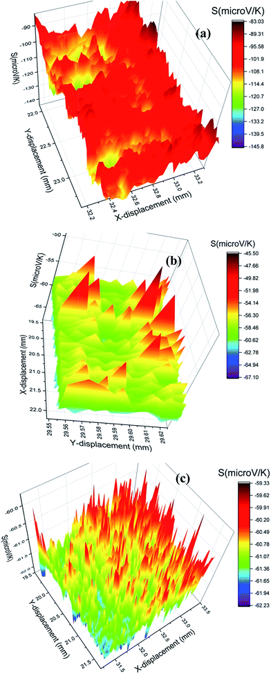 |
| | Fig. 4 Spatial distribution of thermopower (S) (a) Dy0.4Co4Sb12, (b) Dy0.1Co0.9Ni0.1Sb3 and (c) Dy0.4Co3.2Ni0.8Sb12 samples. | |
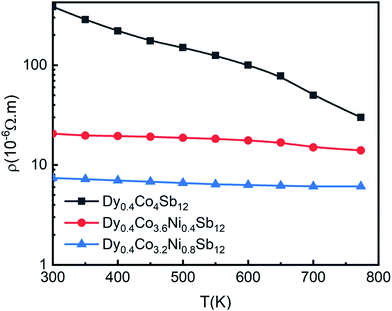
3.3 Electrical resistivity
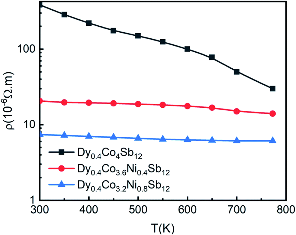
In order to understand the effect of Ni doping and bimodal grain size distribution on the TE properties, the temperature dependent electrical resistivity (ρ) of Dy0.4Co4Sb12, Dy0.4Co3.6Ni0.4Sb12 and Dy0.4Co3.2Ni0.8Sb12 samples from 300 K to 773 K is measured as shown in Fig. 5. It shows the narrowband gap semiconductor of the Dy0.4Co4Sb12 sample. Electrical resistivity (ρ) continuously decreases with an increase in Ni concentration. It may be due to the fact that Ni gives extra free charge carriers/electrons to the Fermi level.41–44 The decrease in ρ in the case of the Dy0.4Co3.2Ni0.8Sb12 sample can also be explained using the bimodal distribution of grains present in the sample. Generally, the dislocations generated during ball milling get localized at the interfaces/grain boundaries in the SPS samples.56 These interfaces act as dominant sources of electron scattering and reduce the electron mean free path. Hence, ρ increases or electrical conductivity decreases. Since Dy0.4Co4Sb12, and Dy0.4Co3.6Ni0.4Sb12 samples consist of equiaxed grains of average size 60 nm, the electron scattering will be more. In contrast, the Dy0.4Co3.2Ni0.8Sb12 sample has both smaller grains of average size 60 nm and larger grains of average size 200 nm. Due to the presence of large grains, the mean free path of the electron increases and hence ρ decreases or conductivity increases in the case of the Dy0.4Co3.2Ni0.8Sb12 sample.
 |
| | Fig. 5 Variation of electrical resistivity (ρ) with T from 300 K to 773 K of the investigated samples, and solid points are the data points and the line is given to guide the data points. | |
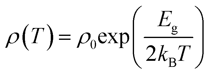
The band gap of the samples in different temperature regions has been calculated using the Arrhenius equation: 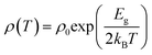 , where, ρ0 is the pre-exponential constant in the fitted region, Eg is the band gap/energy gap and kB is the Boltzmann constant.7 The experimental data are fitted using the linear equation of ln(ρ) and 1000/T. In the case of Dy0.4Co4Sb12, Eg is 120 and 470 meV at 300–550 K and 600–773 K temperature respectively. The increase in the band gap with an increase in T can be explained by the report of Singh et al.31 In the extrinsic/doped semiconductor like skutterudites, at low T, the extrinsic carriers mostly dominate conduction. When T is increased, the extrinsic carriers deplete and the conduction is mostly due to intrinsic carriers only and hence the band gap increases. The 470 meV in the higher temperature region can be related to the indirect pseudoband gap.31Eg is reduced significantly in Ni doped samples (Dy0.4Co3.6Ni0.4Sb12) compared to the undoped sample (Dy0.4Co4Sb12). The Eg of Dy0.4Co3.6Ni0.4Sb12 is 10 and 72 meV at 300–550 K and 600–773 K respectively. The Dy0.4Co3.6Ni0.4Sb12 sample behaves like a narrow bandgap semiconductor.57 The value of Eg in the case of the Dy0.4Co3.2Ni0.8Sb12 sample between 300 K and 773 K is evaluated to be 30 meV. Hence, the Dy0.1Co0.8Ni0.2Sb3 sample behaves like an electron crystal, where the decrease in ρ with an increase in T is minimal. On the other hand it can be concluded that the electrons face minimal scattering at higher T. This may be due to the increase in the electronic mean free path because of the presence of bimodal size distribution of the grains in the Dy0.4Co3.2Ni0.8Sb12 sample as discussed above. The ρ of the Dy0.4Co3.2Ni0.8Sb12 sample at 300 K is 7.4 × 10⁻⁶ Ω m and at 773 K it is 6.1 × 10⁻⁶ Ω m. Hence the change of ρ of the Dy0.4Co3.2Ni0.8Sb12 sample is ∼17% between 300 K and 773 K. The decrease in the band gap with an increase in Ni doping is due to the quantum mechanical tunneling of the electron as discussed elsewhere.58–60 When Ni is doped in place of Co, the barrier width (r0) and the depth of its nearest potential well (W) are reduced while the transmission probability increases.53 The transmission probability of electron tunneling through a scattering potential barrier is expressed by the equation
  , where m* is the effective mass of the electron, and h is Planck's constant.31–33 With Ni doping, the barrier width and potential well decrease and hence the transmission probability increases.53
3.4 Thermopower, carrier concentration and power factor
In order to know the effect of Ni doping in Dy0.4Co4Sb12 on the absolute thermopower (S), the S values of Dy0.4Co4Sb12, Dy0.4Co3.6Ni0.4Sb12 and Dy0.4Co3.2Ni0.8Sb12 samples have been investigated from 300 K to 773 K (Fig. 6(a)). The room temperature S values of all the samples are higher than the values measured by PSM. In the case of Dy0.4Co4Sb12, S increases up to 500 K and then decreases due to the bipolar effect of electrons and holes.16,22,23 Hence, it can be concluded that both S and ρ decrease with an increase in Ni doping due to the increase of carrier concentration as S and ρ are inversely proportional to the carrier concentration.17,18 A similar behavior of the thermopower for n-type undoped CoSb3 is reported earlier.41,42,44,52 For the Ni doped samples (Dy0.4Co3.6Ni0.4Sb12 and Dy0.4Co3.2Ni0.8Sb12), S increases with an increase in T. When Ni is doped in place of Co, it contributes a higher number of n-type carriers (electrons) and hence the bipolar effect is almost suppressed till 773 K. Therefore, the drive for thermopower (S) reduction starts at higher temperature for Dy0.4Co3.6Ni0.4Sb12 and Dy0.1Co0.8Ni0.2Sb3 samples. On the other hand, the Hall effect measurements done by various authors clearly indicate that electrons are the majority charge carriers in Ni doped CoSb3 skutterudites.41–44,54,55 It is reported that Ni-doping at the Co site reduces the electrical resistivity much more than that of doping with other elements.19 Hence, Ni doping helps to improve the electrical conductivity to a large extent and reduces the bipolar effect of thermopower in skutterudites. In the case of the Dy0.4Co4Sb12 sample, the S value attains a peak ∼200 μV at 500 K, suggesting that the Dy0.4Co4Sb12 sample has a thermal bandgap (ES) of ∼200 meV (ES = 2eSmaxTmax, where Smax is the maximum value of S attained in the sample and Tmax is the temperature where S attains Smax).52 On the other hand, S increases with an increase in T in the case of Ni doped samples. A similar behavior of S with T is also reported earlier in Ni doped skutterudites synthesized by other routes.52 For the case of Ni doped samples, the effect of bipolar compensation is suppressed till 773 K. This indicates that with an increase in Ni doping concentration, the onset of the weak bipolar effect shifts to higher temperature (above 773 K). It is known that partial doping of Ni in the Co site in pure CoSb3 makes the majority charge carriers from holes to electrons.52 In the case of Dy0.4Co3.6Ni0.4Sb12 and Dy0.4Co3.2Ni0.8Sb12 samples, where more than one type of independent charge carrier is present, S can be expressed as52 , where ρi and Si are the partial electrical resistivity and partial thermopower respectively. ρin and Sin are the partial electrical resistivity and partial thermopower due to intrinsic charge carriers respectively. ρNi and SNi are partial electrical resistivity and partial thermopower due to Ni doping. The reduction of extrinsic carriers at high temperature leads to the bipolar effect of S. Hence the p-type intrinsic carrier of non-doped CoSb3 would dominate the weighting factor
  of electrical resistivity and hence S begins to decrease. However, the Ni-doping leads to a significant increase of extrinsic n-type carrier concentration (Table 1). Hence, the depletion of n-type extrinsic charge carriers would be shifted to higher temperatures in the case of Dy0.4Co3.6Ni0.4Sb12 and Dy0.4Co3.2Ni0.8Sb12 samples (Fig. 6(a)). Since in Ni doped skutterudites, the majority carriers are electrons, the weighting factor to decrease ρ is dominated by the electrons contributed by Ni-doping, and hence electrons too dominate the S of Dy0.4Co3.6Ni0.4Sb12 and Dy0.4Co3.2Ni0.8Sb12 samples. Besides, the decrease of ρ is more significant in the Dy0.4Co3.2Ni0.8Sb12 sample. It may be concluded that Ni doping in Dy0.4Co4Sb12 would significantly decrease ρ thus reducing the bipolar effect of S. The carrier concentration (n) is calculated by fitting Mott's equation (
 are the Boltzmann constant, Planck's constant and effective mass respectively)59 to the S–T data and is tabulated in Table 1. It reveals that ‘n’ increases drastically with an increase in Ni doping. For calculation, m* is considered to be equal to me (mass of the electron). The ‘n’ and mobility (μ) were also evaluated from the measured Hall co-efficient (RH) and resistivity (ρ) data. The ‘n’ values of Dy0.4Co4Sb12, Dy0.4Co3.6Ni0.4Sb12 and Dy0.4Co3.2Ni0.8Sb12 samples are evaluated to be 0.26 × 1020 cm−3, 0.86 × 1020 cm−3 and 2.66 × 1020 cm−3 respectively. Although these values are slightly lower than the ‘n’ value calculated from ‘S’ data using Mott's formula, there is also a drastic increase in ‘n’ with an increase in Ni concentration. On the other hand the ‘μ’ values of Dy0.4Co4Sb12, Dy0.4Co3.6Ni0.4Sb12 and Dy0.4Co3.2Ni0.8Sb12 samples are calculated to be 6.2 cm2 V−1 S−1, 35.3 cm2 V−1 S−1 and 31.7 cm2 V−1 S−1 respectively. The ‘μ’ value increases from the Dy0.4Co4Sb12 sample to the Dy0.4Co3.6Ni0.4Sb12 sample and then decreases slightly in the case of the Dy0.4Co3.2Ni0.8Sb12 sample. The slight decrease in ‘μ’ in the case of the Dy0.4Co3.2Ni0.8Sb12 sample may be due to the scattering at the bimodal distribution of grains present in the sample.
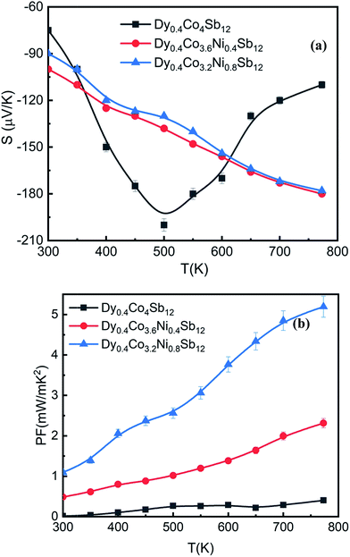 |
| | Fig. 6 Variation of (a) thermopower (S) with T and (b) the power factor (PF) with T of the investigated samples, and solid points are the data points and the line is given to guide the data points. | |
Fig. 6(b) shows the power factor (PF = S2/ρ) of the investigated samples. The highest PF achieved in the Dy0.4Co3.2Ni0.8Sb12 sample is 5.2 mW mK−2, which is the highest PF reported for skutterudites so far.53 The highest PF comes from the many fold decrease of electrical resistivity while maintaining the moderate thermopower of the Ni doped sample (Dy0.4Co3.2Ni0.8Sb12).
3.5 Thermal conductivity
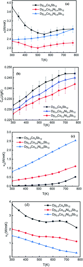
The variation of thermal conductivity (κ) with T (Fig. 7(a)) and specific heat capacity (CP) with T (Fig. 7(b)) of the investigated samples from 300 K to 773 K shows that κ decreases with an increase in T. At 300 K, the CP values of all the samples are close to 0.23 J g−1 K−1. Our κ values are comparable to those of other Ni doped CoSb3 samples reported so far.41–45,53 At 300 K, the κ values of Dy0.4Co4Sb12, Dy0.4Co3.6Ni0.4Sb12 and Dy0.4Co3.2Ni0.8Sb12 samples are 3.8, 2.3 and 2.35 W mK−1 respectively. Unlike the electrical conductivity increase with an increase in Ni, κ is not enhanced much with an increase in Ni. Since κ = κe + κL, where κe is the electronic contribution to κ and κL is the lattice contribution to κ. From the Wiedmann Frantz law, κe = LT/ρ, where L is the Lorentz constant ∼ 2 × 10⁻⁸ V2 K−2 for a degenerate semiconductor.7 The electronic and lattice thermal conductivity are plotted in Fig. 7(c) and (d) respectively. It is observed that κ is mostly the contribution from κe in Ni doped samples. The electronic conductivity increases with an increase in T whereas the lattice thermal conductivity decreases with an increase in T. In the case of the Dy0.4Co4Sb12 sample, the electronic part is 4% at 773 K whereas Dy0.4Co3.6Ni0.4Sb12 and Dy0.4Co3.2Ni0.8Sb12 samples have 8.7% and 75% of total κ respectively. Ni doping enhances κe, and hence the major part of the thermal conductivity is due to the electronic contribution in Ni doped samples especially when the Ni concentration is higher (Dy0.4Co3.2Ni0.8Sb12 sample). The value of κL at 773 K is 2.1 W mK−1, 1.2 W mK−1 and 0.3 W mK−1 for Dy0.4Co4Sb12, Dy0.4Co3.6Ni0.4Sb12 and Dy0.4Co3.2Ni0.8Sb12 samples, respectively. Here it might be assumed that Ni dopants act as strong phonon scattering centers to affect the κL at higher T.34 In addition, Sb vacancies also act as phonon blockers and reduce the lattice thermal conductivity.62 It can be calculated that phonon scattering rates in Ni doped samples increase due to the increase of structural point-defect scattering (due to Ni doping and Sb vacancies) and grain boundary scattering.61 In addition, the bimodal distribution of grains in the Dy0.4Co3.2Ni0.8Sb12 sample might act as phonon filters and hence the lattice thermal conductivity reduces drastically. Hence the Ni doped samples especially Dy0.4Co3.2Ni0.8Sb12 act as phonon-glass systems. Previous work on skutterudite TE materials shows that filling the skutterudite cages with multiple RE elements enhances phonon scattering.4–9 In our case, we could manage to get phonon glass behavior by single RE filling and increasing the Ni doping concentration. Table 2 summarizes the κL value of Dy0.4Co3.2Ni0.8Sb12 at 773 K for the investigated samples and the earlier reported best results on skutterudites for better comparison.36,37
 |
| | Fig. 7 (a) Variation of thermal conductivity (κ) with T of the investigated samples, and solid points are the data points and the line is given to guide the data points. (b) Variation of specific heat capacity (CP) with T of the investigated samples, and solid points are the data points and the line is given to guide the data points. (c) Variation of electronic thermal conductivity (κe) with T of the investigated samples, and solid points are the data points and the line is given to guide the data points. (d) Variation of lattice thermal conductivity (κL) with T of the investigated samples, and solid points are the data points and the line is given to guide the data points. | |
Table 2 Comparison of the lattice thermal conductivity and figure of merit (ZT) of the Dy0.4Co3.2Ni0.8Sb12 sample with the reported values at 773 K. The best reported results have been mentioned
| Sample |
κ
L (W mK−1) |
ZT
|
| Dy0.4Co3.2Ni0.8Sb12 (this work) |
0.3 |
1.4 |
| Co0.9Ni0.1Sb3 (ref. 37) |
4.8 |
0.0004 |
| Co3.9Ni0.1Sb11.5Te0.4Se0.1 (ref. 41) |
1.7 |
1.1 |
| Ce0.8Fe3.5Ni0.5Sb12 (ref. 62) |
1.4 |
0.77 |
3.6 Figure of merit
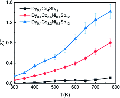
A reasonably higher PF combined with reduced thermal conductivity leads to an enhancement of the figure of merit (ZT) in Dy0.4Co3.2Ni0.8Sb12.Fig. 8 shows the temperature dependence of the thermoelectric figure-of-merit ZT (=S2T/ρκ) of the investigated samples. The ZT value increases with increasing temperature from 300 K to 773 K. The ZT is 0.12, 0.8 and 1.4 at 773 K for the Dy0.4Co4Sb12, Dy0.4Co3.6Ni0.4Sb12 and Dy0.4Co3.2Ni0.8Sb12 samples, respectively. There is an uncertainty of ± 10% in the measurement of ZT. The value of ZT = 1.4 ± 0.14 is one of the highest values for the n-type single element filled cobalt skutterudites fabricated using a solid state reaction.27–29,38
 |
| | Fig. 8 Variation of the figure of merit (ZT) with T of the investigated samples, and solid points are the data points and the line is given to guide the data points. The error bar is given to know the average ZT values of the investigated samples. | |
3.7 Mechanical properties
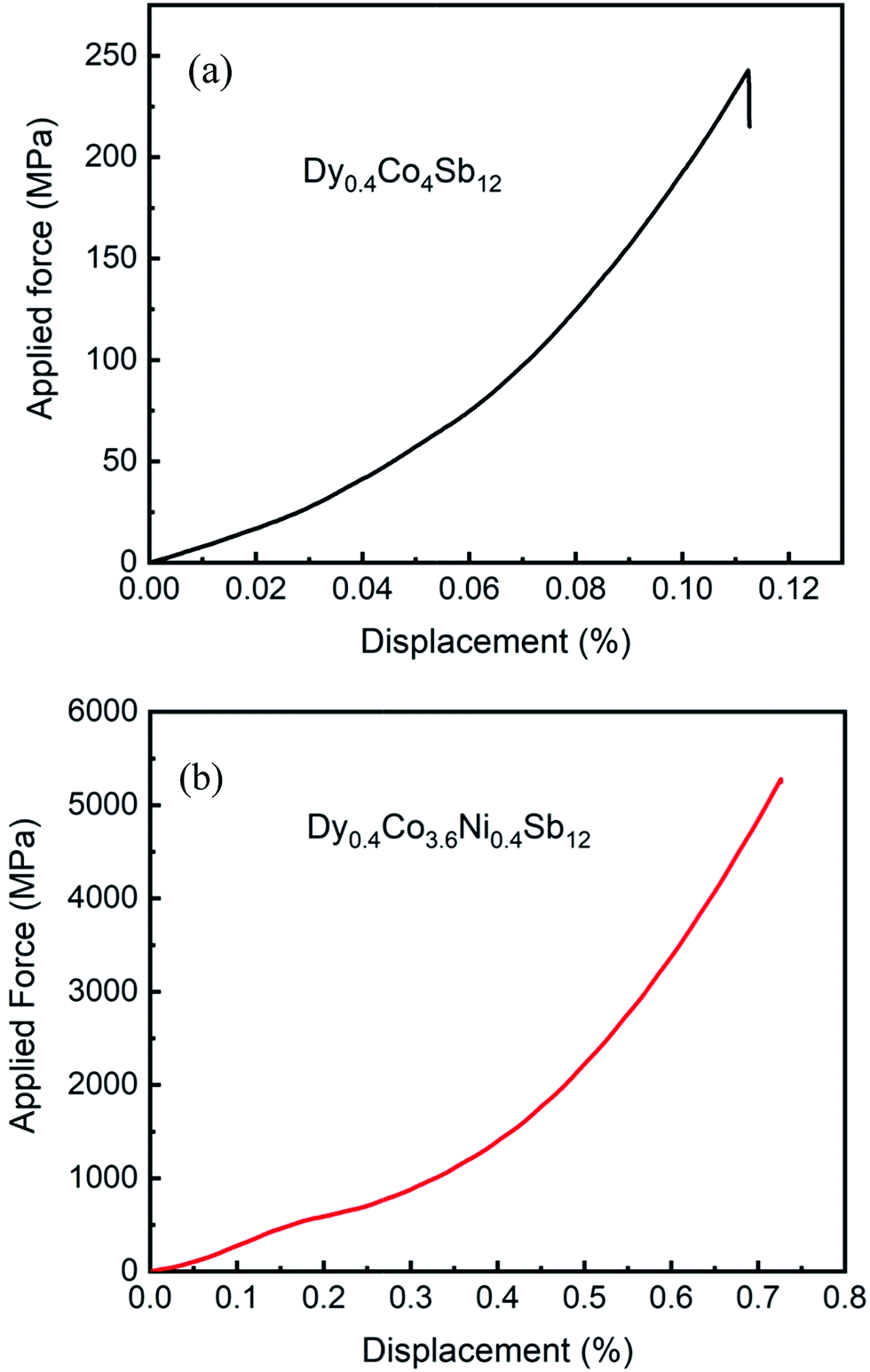
In order to investigate the effect of Ni doping on the mechanical properties of Dy0.4Co4Sb12 samples, the compression test was performed on Dy0.4Co4Sb12 and Dy0.4Co3.6Ni0.4Sb12 samples at 773 K at a strain rate of 0.0001/s. The applied force vs. displacement curve (Fig. 9) shows that the Dy0.4Co4Sb12 sample fails at 250 MPa applied force with 0.12% displacement. On the other hand, the Dy0.4Co3.6Ni0.4Sb12 sample did not fail till 5500 MPa applied force and the displacement of the sample is 0.7%. This means that the Dy0.4Co3.6Ni0.4Sb12 sample is not brittle at 773 K. This confirms that Ni doping helps to improve the mechanical properties of Dy0.4Co4Sb12 skutterudite thermoelectric materials.
 |
| | Fig. 9 Variation of applied force vs. displacement of (a) Dy0.4Co4Sb12 and (b) Dy0.4Co3.2Ni0.8Sb12 samples at 773 K. | |
4 Conclusions
In summary, Dy filled Ni doped CoSb3 skutterudites were synthesized using a ball milling and spark plasma sintering technique. The samples are of single skutterudite phase and consist of nanometer sized grains. Recrystallized elongated grains are observed in the Dy0.4Co3.2Ni0.8Sb12 sample. Ni doping reduces the electrical resistivity by decreasing the band gap at the Fermi level. The thermopower of the Ni doped skutterudites did not alter much compared to the non-doped sample. On the other hand, Ni dopants in place of Co act as point defect scattering centres to reduce the lattice thermal conductivity drastically. Point defect scattering due to Ni doping and bimodal grain size distribution in the Dy0.4Co3.2Ni0.8Sb12 sample leads to drastic reduction of lattice thermal conductivity. As a result, a higher figure of merit of ∼1.4 ± 0.14 at 773 K is achieved in the Dy0.4Co3.2Ni0.8Sb12 sample. The figure of merit appears to be the highest among those of the single element filled CoSb3 skutterudites reported so far at this temperature. The mechanical testing shows the enhancement of mechanical strength in Ni doped samples. Hence, Ni doped CoSb3 skutterudites are of scientific and technological importance in thermoelectric device applications.
Conflicts of interest
There are no conflicts to declare.
Acknowledgements
The authors are grateful to the Director, ARCI for his continuous support. The authors would like to thank Prof. G. Sundararajan, Distinguished Scientist, ARCI for his keen interest in carrying out this work. The authors would like to thank NTBN Koundinya and Prof R S Kottadda of IIT Madras, Chennai for providing the tensile testing facility. The authors are grateful to Dr Kanishka Biswas of JNCASR, Bangalore for providing the room temperature Hall measurement facility. The authors are also grateful to DST for the financial support through a research grant (No. AI/1/65/ARCI/2014). U. Goutham of CAEM (ARCI) is highly acknowledged for his valuable help in experiments.
References
- K. Kirievsky, M. Shlimovich, D. Fuks and Y. Gelbstein, Phys. Chem. Chem. Phys., 2014, 16, 20023–20029 RSC.
- K. Kirievsky, Y. Gelbstein and D. Fuks, J. Solid State Chem., 2013, 203, 247–254 CrossRef CAS.
- G. Rogl, P. Sauerschnig, Z. Rykavets, V. V. Romaka, P. Heinrich, B. Hinterleitner, A. Grytsiv, E. Bauer and P. Rogl, Acta Mater., 2017, 131, 336–348 CrossRef CAS.
- H. Zhang, Y. Wang, K. Dahal, J. Mao, L. Huang, Q. Zhang and Z. Ren, Acta Mater., 2016, 113, 41–47 CrossRef CAS.
- G. Rogl, A. Grytsiv, P. Heinrich, E. Bauer, P. Kumar, N. Peranio, O. Eibl, J. Horky, M. Zehetbauer and P. Rogl, Acta Mater., 2015, 91, 227–238 CrossRef CAS.
- G. Rogl, A. Grytsiv, P. Rogl, N. Peranio, E. Bauer, M. Zehetbauer and O. Eibl, Acta Mater., 2014, 63, 30–43 CrossRef CAS.
- M. Battabyal, B. Priyadarshini, D. Sivaprahasam, N. Karthiselva and R. Gopalan, J. Phys. D: Appl. Phys., 2015, 48, 455309 CrossRef.
- M. Battabyal, B. Priyadarshini, L. Pradipkanti, D. K. Satapathy and R. Gopalan, AIP Adv., 2016, 6, 075308 CrossRef.
- Y. Sadia, L. Dinnerman and Y. Gelbstein, J. Electron. Mater., 2013, 42(7), 1926–1931 CrossRef CAS.
- Y. Gelbstein, J. Tunbridge and R. Dixon,
et al.
, J. Electron. Mater., 2014, 43(6), 1703–1711 CrossRef CAS.
- Y. Rosenberg, Y. Gelbstein and M. P. Dariel, J. Alloys Compd., 2012, 526, 31–38 CrossRef CAS.
- Y. Gelbstein, Z. Dashevsky and M. P. Dariel, Phys. Rev. B: Condens. Matter Mater. Phys., 2007, 396, 16–21 CrossRef CAS.
- Y. Gelbstein and J. Davidow, Phys. Chem. Chem. Phys., 2014, 16(37), 20120–20126 RSC.
- Y. Gelbstein, Acta Mater., 2013, 61(5), 1499–1507 CrossRef CAS.
- E. S. Toberer, C. A. Cox, S. R. Brown, T. Ikeda, A. F. May, S. M. Kauzlarich and G. J. Snyder, Adv. Funct. Mater., 2008, 18, 2795–2800 CrossRef CAS.
- G. S. Nolas, D. T. Morelli and T. M. Tritt, Annu. Rev. Mater. Sci., 1999, 29, 89–116 CrossRef CAS.
-
D. M. Rowe, Handbook of Thermoelectrics, CRC Press, Boca Raton, 1995 Search PubMed.
- B. C. Sales, D. Mandrus and R. K. Williams, Science, 1996, 272, 1325–1328 CrossRef CAS PubMed.
- B. C. Sales, D. Mandrus, B. C. Chakoumakos, V. Keppens and J. R. Thompson, Phys. Rev. B: Condens. Matter Mater. Phys., 1997, 56, 15081–15089 CrossRef CAS.
- B. Matt and A. VanderGraaff, J. Appl. Phys., 2017, 121, 205105 CrossRef.
-
G. S. Nolas, The Physics and Chemistry of Inorganic Clathrates, Springer Series in Materials Science, vol. 199, Springer-Verlag, 2014 Search PubMed.
- G. S. Nolas, J. Poon and M. Kanatzidis, MRS Bull., 2006, 31, 199–205 CrossRef CAS.
- X. Shi, J. Yang, J. R. Salvador, M. Chi, J. Y. Cho, H. Wang, S. Bai, J. Yang, W. Zhang and L. Chen, J. Am. Chem. Soc., 2011, 133(20), 7837–7846 CrossRef CAS PubMed.
- X. Shi, H. Kong, C. P. Li, C. Uher, J. Yang, J. R. Salvador, H. Wang, L. Chen and W. Zhang, Appl. Phys. Lett., 2008, 92, 182101 CrossRef.
- Z.-G. Chen, G. Han, L. Yang, L. Cheng and J. Zou, Prog. Nat. Sci.: Mater. Int., 2012, 22(6), 535–549 CrossRef.
- Z. Zhou, C. Uher, A. Jewell and T. Caillat, Phys. Rev. B, 2005, 71(23), 235209 CrossRef.
- J. Yang, D. T. Morelli, G. P. Meisner, W. Chen, J. S. Dyck and C. Uher, Phys. Rev. B, 2003, 67(16), 165207 CrossRef.
- J. Yang, G. P. Meisner, D. T. Morelli and C. Uher, Phys. Rev. B, 2000, 63(1), 014410 CrossRef.
- L. Bertini, C. Stiewe, M. Toprak, S. Williams, D. Platzek, A. Mrotzek, Y. Zhang, C. Gatti, E. Müller and M. Muhammed, J. Appl. Phys., 2003, 93(1), 438–447 CrossRef CAS.
- G. Rogl, A. Grytsiv, E. Bauer, P. Rogl and M. Zehetbauer, Intermetallics, 2009, 06, 005 Search PubMed.
- D. J. Singh and W. E. Pickett, Phys. Rev. B: Condens. Matter Mater. Phys., 1994, 50, 11235–11238 CrossRef CAS.
- L. Chapon, D. Ravot and J. C. Tedenac, J. Alloys Compd., 2000, 299, 68–71 CrossRef CAS.
- T. Morimura and M. Hasaka, Scr. Mater., 2003, 48, 495–500 CrossRef CAS.
- R. Viennois, D. Ravot, J. C. Tedenac, S. Charar and A. Mauger, J. Mater. Sci. Eng. B, 2005, 119(1), 1–12 CrossRef.
- L. Chapon, D. Ravot and J. C. Tedenac, J. Alloys Compd., 1999, 282, 58–63 CrossRef CAS.
- D. Bérardan, E. Alleno, C. Godart, M. Puyet, B. Lenoir, R. Lackner, E. Bauer, L. Girard and D. Ravot, J. Appl. Phys., 2005, 98, 033710 CrossRef.
- H. Kitagawa, M. Wakatsuki, H. Nagaoka, H. Noguchi, Y. Isoda, K. Hasezaki and Y. Noda, J. Phys. Chem. Solids, 2005, 66, 1635–1639 CrossRef CAS.
- S. Katsuyama, M. Watanabe, M. Kuroki, T. Maehata and M. Ito, J. Appl. Phys., 2003, 93, 2758–2764 CrossRef CAS.
- M. Puyet, B. Lenoir, A. Dauscher, C. Candolfi, J. Hejtmanek, C. Stiewe and E. Muller, Appl. Phys. Lett., 2012, 101, 222105 CrossRef.
- J. S. Dyck, W. D. Chen, C. Uher, L. Chen, X. F. Tang and T. Hirai, J. Appl. Phys., 2002, 91, 3698 CrossRef CAS.
- C. Xu, B. Duan, S. Ding, P. Zhai and Q. Zhang, J. Electron. Mater., 2014, 43, 6 Search PubMed.
- C. Stiewe, L. Bertini and M. Toprak,
et al.
, J. Appl. Phys., 2005, 97, 044317 CrossRef.
- S. Choi, K. Kurosaki, Y. Ohishi, H. Muta and S. Yamanaka, J. Appl. Phys., 2005, 115, 023702 CrossRef.
- W.-S. Liu, B.-P. Zhang, J.-F. Li, H.-L. Zhang and Li-D. Zhao, J. Appl. Phys., 2007, 102, 103717 CrossRef.
- S. Lee, K. H. Lee, Y.-M. Kim, H. S. Kim, G. J. Snyder, S. Baik and S. Wng Kim, Acta Mater., 2018, 142, 8–17 CrossRef CAS.
- W. S. Liu, Bo P. Zhang, J. F. Li, H. L. Zhang and Li-D. Zhao, J. Appl. Phys., 2007, 102, 103717 CrossRef.
- K. T. Wojciechowski, J. Tobala and J. Leszczyński, J. Alloys Compd., 2003, 361, 19–27 CrossRef CAS.
- A. Majumdar, Science, 2004, 303(5659), 777–778 CrossRef CAS PubMed.
- D. M. Rowe, V. S. Shukla and N. Savvides, Nature, 1981, 290(5809), 765–766 CrossRef CAS.
- Z.-G. Chen, G. Han, L. Yang, L. Cheng and J. Zou, Prog. Nat. Sci.: Mater. Int., 2012, 22(6), 535–549 CrossRef.
- H. Hao, W. Jiang, G. Xie, G. Zhang, Y. Lu, J. Zhang and L. Lou, Prog. Nat. Sci.: Mater. Int., 2013, 23(2), 211–215 CrossRef.
- J. Prado-Gonjal, F. Serrano-Sánchez, N. M. Nemes, O. J. Dura, J. L. Martínez, M. T. Fernández-Díaz, F. Fauth and J. A. Alonso, Appl. Phys. Lett., 2017, 111, 083902 CrossRef.
- A. Gharleghi, Yu-H. Chu, F.-H. Lin, Z.-R. Yang, Yi-H. Pai and C.-J. Liu, ACS Appl. Mater. Interfaces, 2016, 8, 5205–5215 CrossRef CAS PubMed.
- A. Gharleghi and C. J. Liu, Rapid Fabrication and Transport Properties of n-Type Co4−xNixSb12via Modified Polyol Process Synthesis Combined with Evacuated- and- Encapsulated Sintering, J. Alloys Compd., 2014, 592, 277–282 CrossRef CAS.
- E. Alleno, E. Zehani and O. Rouleau, J. Alloys Compd., 2013, 572, 43–48 CrossRef CAS.
- S. Patra, Gouthama and K. Mondal, Prog. Nat. Sci.: Mater. Int., 2014, 24, 608–622 CrossRef CAS.
- R. H. Fowler and L. Nordheim, Proc. R. Soc. London, Ser. A, 1928, 119(781), 173–181 CrossRef CAS.
- M. Lenzlinger and E. H. Snow, Fowler-Nordheim, J. Appl. Phys., 1969, 40, 278–282 CrossRef CAS.
- E. Jacques, L. Pichon, O. Debieu and F. Gourbilleau, Nanoscale, 2011, 6(1), 170 CrossRef PubMed.
- A. Ghosh and S. Chakrabarty, Fowler-Nordheim, Mon. Not. R. Astron. Soc., 2011, 1–9 Search PubMed.
-
N. F. Mott and E. A. Davis, Electronics Processes in Non-crystalline Materials, Clarendon, Oxford, 1971 Search PubMed.
- W.-M. Lee, D.-K. Shin and I.-H. Kim, J. Electron. Mater., 2016, 45, 1245–1250 CrossRef CAS.
|
| This journal is © The Royal Society of Chemistry 2018 |
Click here to see how this site uses Cookies. View our privacy policy here. 
 *a,
Priyadarshini
Balasubramanian
a,
G. Mohan
Muralikrishna
b,
Pawan Kumar
Jain
c and
Raghavan
Gopalan
a
*a,
Priyadarshini
Balasubramanian
a,
G. Mohan
Muralikrishna
b,
Pawan Kumar
Jain
c and
Raghavan
Gopalan
a


 , where, ρ0 is the pre-exponential constant in the fitted region, Eg is the band gap/energy gap and kB is the Boltzmann constant.7 The experimental data are fitted using the linear equation of ln(ρ) and 1000/T. In the case of Dy0.4Co4Sb12, Eg is 120 and 470 meV at 300–550 K and 600–773 K temperature respectively. The increase in the band gap with an increase in T can be explained by the report of Singh et al.31 In the extrinsic/doped semiconductor like skutterudites, at low T, the extrinsic carriers mostly dominate conduction. When T is increased, the extrinsic carriers deplete and the conduction is mostly due to intrinsic carriers only and hence the band gap increases. The 470 meV in the higher temperature region can be related to the indirect pseudoband gap.31Eg is reduced significantly in Ni doped samples (Dy0.4Co3.6Ni0.4Sb12) compared to the undoped sample (Dy0.4Co4Sb12). The Eg of Dy0.4Co3.6Ni0.4Sb12 is 10 and 72 meV at 300–550 K and 600–773 K respectively. The Dy0.4Co3.6Ni0.4Sb12 sample behaves like a narrow bandgap semiconductor.57 The value of Eg in the case of the Dy0.4Co3.2Ni0.8Sb12 sample between 300 K and 773 K is evaluated to be 30 meV. Hence, the Dy0.1Co0.8Ni0.2Sb3 sample behaves like an electron crystal, where the decrease in ρ with an increase in T is minimal. On the other hand it can be concluded that the electrons face minimal scattering at higher T. This may be due to the increase in the electronic mean free path because of the presence of bimodal size distribution of the grains in the Dy0.4Co3.2Ni0.8Sb12 sample as discussed above. The ρ of the Dy0.4Co3.2Ni0.8Sb12 sample at 300 K is 7.4 × 10⁻⁶ Ω m and at 773 K it is 6.1 × 10⁻⁶ Ω m. Hence the change of ρ of the Dy0.4Co3.2Ni0.8Sb12 sample is ∼17% between 300 K and 773 K. The decrease in the band gap with an increase in Ni doping is due to the quantum mechanical tunneling of the electron as discussed elsewhere.58–60 When Ni is doped in place of Co, the barrier width (r0) and the depth of its nearest potential well (W) are reduced while the transmission probability increases.53 The transmission probability of electron tunneling through a scattering potential barrier is expressed by the equation
 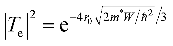 , where m* is the effective mass of the electron, and h is Planck's constant.31–33 With Ni doping, the barrier width and potential well decrease and hence the transmission probability increases.53
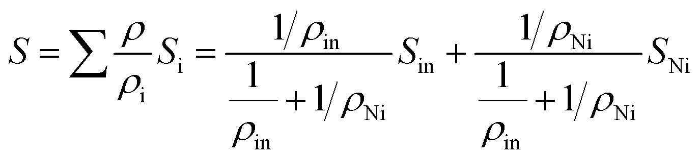 , where ρi and Si are the partial electrical resistivity and partial thermopower respectively. ρin and Sin are the partial electrical resistivity and partial thermopower due to intrinsic charge carriers respectively. ρNi and SNi are partial electrical resistivity and partial thermopower due to Ni doping. The reduction of extrinsic carriers at high temperature leads to the bipolar effect of S. Hence the p-type intrinsic carrier of non-doped CoSb3 would dominate the weighting factor
  of electrical resistivity and hence S begins to decrease. However, the Ni-doping leads to a significant increase of extrinsic n-type carrier concentration (Table 1). Hence, the depletion of n-type extrinsic charge carriers would be shifted to higher temperatures in the case of Dy0.4Co3.6Ni0.4Sb12 and Dy0.4Co3.2Ni0.8Sb12 samples (Fig. 6(a)). Since in Ni doped skutterudites, the majority carriers are electrons, the weighting factor to decrease ρ is dominated by the electrons contributed by Ni-doping, and hence electrons too dominate the S of Dy0.4Co3.6Ni0.4Sb12 and Dy0.4Co3.2Ni0.8Sb12 samples. Besides, the decrease of ρ is more significant in the Dy0.4Co3.2Ni0.8Sb12 sample. It may be concluded that Ni doping in Dy0.4Co4Sb12 would significantly decrease ρ thus reducing the bipolar effect of S. The carrier concentration (n) is calculated by fitting Mott's equation (
 are the Boltzmann constant, Planck's constant and effective mass respectively)59 to the S–T data and is tabulated in Table 1. It reveals that ‘n’ increases drastically with an increase in Ni doping. For calculation, m* is considered to be equal to me (mass of the electron). The ‘n’ and mobility (μ) were also evaluated from the measured Hall co-efficient (RH) and resistivity (ρ) data. The ‘n’ values of Dy0.4Co4Sb12, Dy0.4Co3.6Ni0.4Sb12 and Dy0.4Co3.2Ni0.8Sb12 samples are evaluated to be 0.26 × 1020 cm−3, 0.86 × 1020 cm−3 and 2.66 × 1020 cm−3 respectively. Although these values are slightly lower than the ‘n’ value calculated from ‘S’ data using Mott's formula, there is also a drastic increase in ‘n’ with an increase in Ni concentration. On the other hand the ‘μ’ values of Dy0.4Co4Sb12, Dy0.4Co3.6Ni0.4Sb12 and Dy0.4Co3.2Ni0.8Sb12 samples are calculated to be 6.2 cm2 V−1 S−1, 35.3 cm2 V−1 S−1 and 31.7 cm2 V−1 S−1 respectively. The ‘μ’ value increases from the Dy0.4Co4Sb12 sample to the Dy0.4Co3.6Ni0.4Sb12 sample and then decreases slightly in the case of the Dy0.4Co3.2Ni0.8Sb12 sample. The slight decrease in ‘μ’ in the case of the Dy0.4Co3.2Ni0.8Sb12 sample may be due to the scattering at the bimodal distribution of grains present in the sample.