
Improvements in printable mesoscopic perovskite solar cells via thinner spacer layers†
Qifei
Wang
a,
Shuang
Liu
a,
Yue
Ming
a,
Yanjun
Guan
a,
Daiyu
Li
a,
Congcong
Zhang
b,
Zhaokui
Wang
 b,
Yaoguang
Rong
a,
Yue
Hu
*a and
Hongwei
Han
*a
b,
Yaoguang
Rong
a,
Yue
Hu
*a and
Hongwei
Han
*a
aMichael Grätzel Center for Mesoscopic Solar Cells, Wuhan National Laboratory for Optoelectronics, Huazhong University of Science and Technology, Wuhan 430074, Hubei, P. R. China. E-mail: yuehu@hust.edu.cn; hongwei.han@mail.hust.edu.cn
bJiangsu Key Laboratory for Carbon-Based Functional Materials and Devices, Institute of Functional Nano and Soft Materials (FUNSOM), Soochow University, Suzhou 215123, China
First published on 19th September 2018
Abstract
Printable mesoscopic perovskite solar cells based on TiO2/ZrO2/carbon mesoporous scaffolds have a promising future in commercialization due to their stability and ease of large-scale manufacturing, in which the mesoporous ZrO2 (mp-ZrO2) spacer is crucial in decreasing charge carrier recombination. To obtain high-performance devices, 2–3 μm thick mp-ZrO2 is usually needed. However, such thickness leads to an increased loading amount of perovskite material and causes problems such as reproducibility, pollution, and waste. Herein, we provide a universal solution to enhance VOC in printable mesoscopic PSCs with thin mp-ZrO2 layers. By depositing a thin layer of Al2O3 using a spraying pyrolysis method, we successfully retard the recombination between the TiO2 and carbon electrode. We further find the modification could down-shift the conduction band minimum (CBM) and increase the carrier transportation. Finally, we successfully reduce the mp-ZrO2 thickness of devices from 3 μm to 1.2 μm while retaining comparable device performance. Thanks to thinner ZrO2 layers, the usage of solvent and PbI2 is also reduced, which makes the device both more cost-efficient and environmentally friendly. This modification strategy will pave the way to the commercialization of printable mesoscopic PSCs with greener and cheaper processes.
Introduction
Since perovskites were first reported in the photovoltaic area, the power conversion efficiency (PCE) of perovskite solar cells (PSCs) has risen from 3.81% in 2009 to a certified 23.3% in 2018.1,2 Such a fast development of PCE has shocked the whole scientific community and attracted lots of interest to perovskite materials. Subsequent studies revealed that perovskite materials exhibit excellent properties for photovoltaic applications, such as tunable direct band gaps, high carrier transport rates, long carrier diffusion lengths, broad absorption ranges of light and low defect density.3–9 In addition, PSCs could be fabricated through simple solution-processes at a low cost. The constantly improving stability and successful trials on scaling-up provide a promising future for PSCs to be commercialized for solar cell uses.Recent years have witnessed PSCs based on lots of different structures (including mesoscopic or planar, formal or inverted) and fabrication methods undergoing fast development in both the PCE and stability.10–13 Among these, a printable triple mesoscopic structure reported by the Han group is drawing increasing attention due to its screen-printing based fabrication process and high stability. The perovskite absorber is hosted in a triple-layer scaffold consisting of mesoporous TiO2, ZrO2 and carbon. By replacing Au with carbon as the counter electrode and omitting hole-conductor materials, the devices based on this structure have advantages of low cost and easy fabrication. In addition, printable triple mesoscopic PSCs use less perovskite and solvent than spin-coating based devices. In recent years, the devices based on printable triple mesoscopic structures have developed rapidly showing a PCE of 15.6% for lab-scale devices, 10.4% for 100 cm2 and an AM 1.5 sunlight stability of over 10![[thin space (1/6-em)]](https://www.rsc.org/images/entities/char_2009.gif) 000 h.9,14,15
000 h.9,14,15
The mp-ZrO2 layer plays an important role in separating the mp-TiO2 and carbon layer, and its thickness closely relates to the open-circuit voltage (VOC) and PCE. With the thickness of mp-ZrO2 increasing from 0 μm to 3 μm, the PCE of devices increases from 4.18% to 14% and the VOC increases from 600 mV to 920 mV, respectively.15 However, thicker mp-ZrO2 layers need more perovskite solution to fill in which causes concerns over the reproducibility of devices and the toxicity of the solvent and lead.
To reduce the thickness of mp-ZrO2 layers, two directions can be taken. One is to select a more insulating material to replace ZrO2. The other is to modify the TiO2 with appropriate materials to decrease the recombination between the TiO2 and carbon layer and accelerate the transportation of carriers. It has been reported that polymers like C60SAM and PCBM:PMMA could effectively passivate the defects in the interface of perovskite/TiO2.16,17 Placing a thin layer of metal oxide materials on the surface of electron transporting layers (ETLs) could also effectively modify the energy band gap and work function which further influences the transportation and recombination properties of carriers.18,19 Representative materials include Al2O3,20 La2O3,21 MgO22 and others. Our group previously deposited Al on the surface of mp-TiO2 layers by vacuum evaporation. After a 500 °C annealing process, the Al oxidized and formed an ultra-thin layer of Al2O3 between the TiO2 and ZrO2. Meanwhile, we also found that the surface of TiO2 was modified with Al2O3 in this way. As a result, the recombination in devices was obviously reduced.20
Compared to vacuum evaporation which needs high vacuum, we further develop a simple spraying pyrolysis method to deposit Al2O3 on the surface of TiO2. We successfully fabricated PSCs using only 1.2 μm thick ZrO2 and reached PCEs over 14%, comparable with the devices using 3 μm thick ZrO2. The 1.2 μm devices showed a better reproducibility than the 3 μm ones using only half the amount of lead and solvent. Through our work, we find that Al2O3 could retard the recombination between the TiO2 and carbon electrode. Besides, more experiments reveal that Al2O3 could down-shift the CBM energy level of TiO2. By utilising thermal admittance spectroscopy, we find the defect density also decreases in modified TiO2. For reducing the recombination and enhancing the VOC of devices, it could be a universal method to modify TiO2 with Al2O3 by a simple spraying pyrolysis method in printable mesoscopic PSCs.
Methods and materials
Materials
All materials were used as received. Lead(II) iodide (PbI2, 99%) was purchased from Acros Organics. Methylammonium iodide (MAI, 99%) was purchased from Materwin of Shanghai. γ-Butyrolactone (GBL, >99.9%) was purchased from Aladdin. Titanium diisopropoxide bis(acetylacetonate) (75 wt% in isopropanol) was purchased from Sigma-Aldrich. The other materials such as isopropanol (99.7%), acetylacetone (99%) and aluminum isopropoxide (chemical purity) were purchased from Sinopharm Chemical Reagent Company.5-Ammoniumvaleric acid iodide was synthesized following previous literature.23
Precursor solution synthesis
Device fabrication
FTO coated glasses were patterned using lasers to form two separated electrodes and subsequently cleaned with detergent, deionized water and ethanol using an ultrasonic cleaner. We sprayed the titanium precursor solution at 450 °C on the surface of cleaned substrates to obtain the compact TiO2 (c-TiO2) layer. After cooling to room-temperature, a 500 nm-thick TiO2 mesoporous (mp-TiO2) layer was screen-printed on the c-TiO2. Al2O3 precursor solution was sprayed on mp-TiO2 at 450 °C in 3 circles (thickness < 2.4 nm) and remained at this temperature for 30 minutes, then was heated to 500 °C and kept at this temperature for 40 minutes. After the devices were cooled down, a mesoporous ZrO2 layer (1.2 μm, 2 μm or 3 μm) and 15 μm carbon layer were screen-printed on the devices. The perovskite precursor solution was dropped on the edge of the carbon layer, then the devices were annealed at 50 °C in an oven for 2 hours.Perovskite film fabrication
TiO2 was deposited on the surface of clean FTO substrate by a screen-printing method and annealed at 500 °C for 40 min. Before the spin-coating process, the TiO2 layer was dealt with by UV irradiation to remove any remaining organic residues. 20 μl of MA0.965(5-AVA)0.035PbI3 precursor solution was spin coated on the substrate of TiO2 at 2000 rpm for 30 s, followed by annealing at 50 °C for 2 hours.Characterization
Scanning electron microscopy (SEM) images of perovskite films and cross-section SEM of devices were attained using a field-emission scanning electron microscope (Nova NanoSEM 450, FEI). Ultraviolet photoelectron spectroscopy (UPS) and X-ray photoelectron spectroscopy (XPS) were performed using a Kratos Axis Ultra DLD system. UV-vis spectra of TiO2 and perovskite films were recorded using a PerkinElmer Lambda950 spectrometer. Thermal admittance spectroscopy (TAS) was performed using a Precision Impedance Analyzer (Agilent 4294A). Steady-state photoluminescence (PL) spectra were measured using a LabRAM HR800 (Horiba Jobin Yvon). Time-resolved PL spectra were recorded using a fluorescence spectrometer (DeltaFlex, Horiba). X-ray diffraction (XRD) spectra were recorded using an X-ray diffractometer (X’pert PRO, Cu Kα radiation, 40 kV) under conditions of 40 mA from 10° to 60° with a scanning speed of 5° per min. Photocurrent density–voltage (J–V) curves were recorded using a Keithley 2400 source meter and a Newport solar simulator (model 91192). The power of the simulated light was calibrated to 100 mW cm−2 using a Newport Oriel PV reference cell (model 91150 V). The active area of the device was 0.8 cm2, and an opaque black mask with a circular aperture (0.108 cm2) was adopted for J–V measurements. The J–V testing was performed in both reverse and forward scan directions at 100 mV s−1 (sweep settling time of 100 ms). The IPCE spectra were measured using a 150 W xenon lamp (Oriel) fitted with a monochromator (Cornerstone 74004) as a monochromatic light source. Calibration with the Oriel Si detector was carried out before IPCE measurements. Unless stated otherwise, all the measurements were carried out at RH ∼ 45% and RT.Results and discussion
The schematic structure of the printable mesoscopic PSCs is shown in Fig. 1a. The devices are based on a mp-TiO2/mp-ZrO2/carbon mesoporous scaffold. In the TiO2 layer, the perovskite absorbs light and excitons are generated. Then the electrons and holes are separated and extracted upon an internal electric field. Perfect energy level alignment ensures enough driving force for charge transport. As shown in Fig. 1b, the ZrO2 layer plays an important spacer role in the structure in separating the TiO2 and carbon electrode and reducing charge recombination. We systematically explored how the thickness of the mesoporous ZrO2 (mp-ZrO2) layer and the filling amount of perovskite precursor solution influence the PCE of PSCs. In Fig. 1c, the average performance of devices with different amounts of precursor solution is exhibited, in which devices were fabricated with 1.2 μm mp-ZrO2, 2 μm mp-ZrO2 and 3 μm mp-ZrO2, respectively. Upon increasing the filling amount of perovskites, we observed an enhanced PCE for all cells regardless of the thickness of ZrO2. This is not surprising because the perovskites need to first fill up all the pores in mp-ZrO2 and mp-TiO2 and form uniform and continuous crystals to ensure sufficient light absorption and good charge transport (Fig. S1†). When 2 μl of perovskite was used, the 1.2 μm devices showed a much higher PCE than the 2 μm and 3 μm ones. The performance remained unchanged when more perovskite was applied, indicating complete pore filling and good crystallinity of perovskite with only 2 μl of perovskite precursor solution. In the case of the 2 μm and 3 μm devices, the saturated amount of perovskite was 3 μl and 4 μl, respectively. Further increases of perovskite will not lead to continuous enhancement of PCE. The reason for this could relate to the transport process of electrons. Once electrons reach the carbon counter electrode, the extra perovskite in the carbon layer does not contribute to electron transportation because carbon conducts much better than perovskite.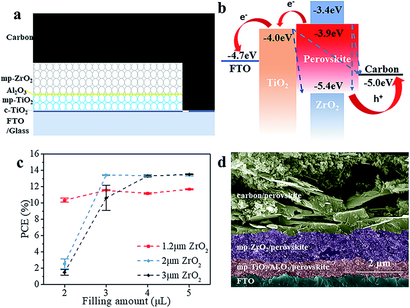 | ||
| Fig. 1 The printable mesoscopic perovskite solar cells. (a) The schematic structure of printable mesoscopic PSCs. (b) Energy level diagrams of the printable mesoscopic PSCs. The red arrows represent effective carrier transport and the blue dashed lines reflect recombination of carriers. (c) The average performance of devices with different amounts of precursor solution. The thickness of the mp-ZrO2 layer is 1.2 μm (red line), 2 μm (blue line) and 3 μm (black line). Five devices were used for each point. (d) The cross-section SEM of a solar cell based on the modified TiO2 layer. | ||
We compared the best performing cells using different thicknesses of ZrO2. As shown in Fig. S2,† all devices exhibit complete pore-filling and continuous crystallinity. With the thickness of mp-ZrO2 layer increasing, the VOC of devices was improved from 0.84 V to 0.92 V. Thicker mp-ZrO2 layers could effectively separate the carbon counter electrode from the mp-TiO2 layer thus reducing the recombination. Accordingly, the average PCE of devices increased from 12.7% (1.2 μm ZrO2) to 13.8% (3 μm ZrO2). However, we observed huge deviation of device performance with 3 μm devices, as shown in Fig. 2a and S3.† The main difference originated from the JSC, as a result of the complex crystallization process in the thick scaffold. The 1.2 μm devices have a much higher reproducibility, however, with the sacrifice of the PCE.
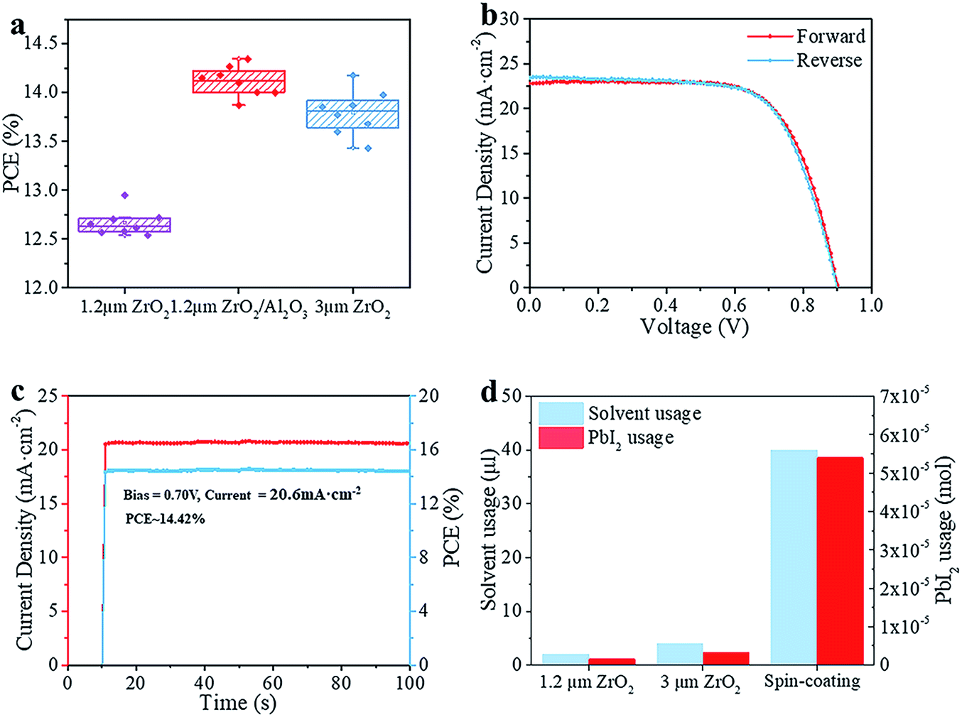 | ||
| Fig. 2 The properties of the devices based on modified TiO2. (a) The performance of devices based on 1.2 μm ZrO2, 1.2 μm ZrO2/Al2O3 and 3 μm ZrO2 layers. For each group, 8 pieces of the device in total were taken into account. (b) J–V curves of the champion device. (c) Stabilized power output measurement of the champion device with a bias voltage of 0.7 V. (d) The usage of solvent and PbI2 in different situations per cell. All the tests were performed after the devices were aged in air (RT > 20 °C, RH > 50%) over two days without sealing. | ||
We adopted a spraying pyrolysis method to modify the mp-TiO2 layer with Al2O3. Spraying pyrolysis has advantages of depositing uniform films of high density over relatively large areas with a well-controlled thickness, flexibility in the choice of precursor materials and their combinations, potential for low cost electronic applications, etc.24,25 The Al2O3 we used in this study was synthesized from aluminium isopropoxide and acetylacetone. The precursor solution of Al2O3 was sprayed on the surface of mp-TiO2 at 450 °C with a chromatography sprayer and the precursor decomposed to Al2O3 under 450 °C. Upon inserting the super thin Al2O3 layer, we observed an obvious VOC enhancement from an average 840 mV to over 890 mV with improvements in the JSC and FF as well, yielding an average PCE beyond 14%.
As shown in Fig. 2b, the champion device exhibits a VOC of 900 mV, JSC of 22.81 mA cm−2, FF of 0.70 and PCE of 14.39% in the forward scan (from JSC to VOC). In the reverse scan (from VOC to JSC), the cell gives a VOC of 900 mV, JSC of 23.45 mA cm−2, FF of 0.68 and PCE of 14.31%. The PCE is 0.08% higher in the forward scan and the whole device exhibits a slight hysteresis compared to the one without Al2O3.26 The defects in the mp-TiO2 layer are reduced effectively upon depositing Al2O3,27 thus the movement of electrons and holes becomes similar in reverse and forward scans, and reduces the hysteresis effect. The difference between the PCE obtained from the reverse scan and forward scan makes it difficult to confirm the reliable PCE of the devices. An effective way is to test the stabilized output of the device, by holding the cell at a fixed voltage near the maximum power point on the J–V curve and measuring the photocurrent generated at this fixed applied bias until it stabilizes.28 Finally, we got a stabilized PCE of 14.42%, as shown in Fig. 2c. The cells showed an excellent stability (Fig. S7†). No drop in performance was observed after storing the devices in a humidity chamber (RH ∼ 60%) for 34 days without any encapsulation. The incident-photon-to-current conversion efficiency (IPCE) is shown in Fig. S4.† The spectrum of external quantum efficiency (EQE) exhibits an integrated JSC of 18 mA cm−2 which is lower than the parameter in the J–V curve. However, this is common in this kind of PSC, and the reason for this could rely on the special structure of the devices.23 In Fig. 2d, we calculated the material usage of devices under different situations, in which devices were fabricated with 1.2 μm ZrO2 and 3 μm ZrO2 and by a spin-coating method. Using the spin-coating method, five devices were fabricated on a 6.25 cm2 substrate with an active area of 0.5 cm2. In printable mesoscopic PSCs, we could fabricate one device with an active area of 0.8 cm2 on a substrate of only 5 cm2. Though a thin layer of perovskite is enough to absorb light in normal PSCs fabricated by the spin-coating method, generally 40 μl precursor solution is needed in order to obtain full coverage and sufficient thickness in a complete device fabrication process. In printable mesoscopic perovskite solar cells in which drop-casting is applied only 4 μl is needed and this number is further reduced in devices based on thinner ZrO2 layers. It is known that metal Pb could damage both the environment and human health while the solvents used in fabricating PSCs are injurious to human health due to reasons of toxicity, penetrability and carcinogenicity. With the usage of precursor solution decreasing, the Pb and solvent used during fabrication of PSCs based on 1.2 μm ZrO2 is half the amount of those fabricated with a 3 μm ZrO2 layer and 1/20 of those fabricated by a spin-coating method. When our method was applied to the fabrication of a 100 cm2 PSC module, we could save 2.31 g PbI2 and 5.3 ml GBL for every single piece of the PSC module without sacrificing the performance, which provides excellent potential in both reducing the fabrication cost and protecting the environment.
In printable PSCs, VOC is determined by the Fermi energy level of the mp-TiO2 and carbon counter electrode, which is related to carrier recombination in devices, such as recombination at interfaces and grain boundaries.29,30 We further explored how the super-thin layer of Al2O3 enhanced the performance of devices. First, to explore the existence of Al2O3, we performed X-ray photoelectron spectroscopy (XPS) on FTO/mp-TiO2/Al2O3 (as shown in Table S1†). The atomic ratio of Al2O3 existing on the surface of the mp-TiO2 layer was ∼0.31%. We observed no difference from SEM photographs either, as shown in Fig. 3c and d. The impact of Al2O3 on perovskite was tested by comparing the perovskite films with the structure of perovskite/Al2O3/mp-TiO2/FTO and perovskite/mp-TiO2/FTO. The X-ray diffraction (XRD) patterns are shown in Fig. 3a. There appear to be no new peaks belonging to Al2O3. This means that the Al2O3 existing in the mp-TiO2 layer belongs to the amorphous phase rather than the crystal phase. The intensity of the perovskite peak was enhanced in the modified TiO2, indicating a better crystallinity of perovskite on modified mp-TiO2. In printable mesoscopic perovskite solar cells, pore-filling could be influenced by many factors, such as filling amount, thickness of the mesoscopic layer, size of the nanoparticles and so on.31 Comparing Fig. 1d with Fig. S2c,† we see no difference between the pore-filling situation of the perovskites. This was further confirmed by the UV-vis absorption spectra of perovskite films on the modified and bare TiO2, where we see no difference in either the absorption band edge or the intensity of absorption (Fig. 3b). Above all, we found that the small amount of Al2O3 existing on the TiO2 does not change the perovskite or mp-TiO2 film in terms of morphology and crystallization. We then performed ultraviolet photoelectron spectroscopy (UPS) and recorded photoluminescence (PL) spectra to reveal the changes in energy level. The PL spectrum is an effective method to reveal the photo-induced charge transfer and recombination process. As shown in Fig. 4a, the perovskite films are deposited on the substrates of glass/FTO/mp-TiO2/Al2O3 and glass/FTO/mp-TiO2. The film with modified TiO2 showed lower intensity of stabilized PL, indicating that the charge transports more effectively before the carrier recombines at the interface and eventually improves the electron extraction rate from the perovskite absorber layer. We further recorded time-resolved PL spectra on the same samples as shown in Fig. 4b. In the glass/FTO/TiO2/Al2O3/perovskite film, the lifetime of the photo-induced carrier was 1.1 ns and the control film of glass/FTO/TiO2/perovskite showed a lifetime of 3.6 ns, confirming that the carriers transport faster on modified TiO2. The results of UPS are shown in Fig. 4c and d. In the high binding energy region, the value of the cutoff point of bare TiO2 was 17.63 eV. Because the energy of He is 21.22 eV, the work function of bare TiO2 is 3.59 eV. The cutoff point in the low binding energy region represents the deviation between the Fermi level and valence band maximum (VBM) energy level. The cutoff point value of bare TiO2 was 3.6 eV, so the valence band position of bare TiO2 was −7.19 eV. We calculated the valence band value of modified TiO2 to be −7.24 eV in the same way. Considering the band gap of TiO2 is 3.2 eV, the CBM of TiO2 decreased by 0.05 eV after modification. With a lower CBM energy level, electrons move from the perovskite to mp-TiO2 with a stronger driving force and the lifetime of carriers would be shorter, which is consistent with the results of the PL. However, CBM shifting to a lower energy level will lead to a lower VOC in general. Considering that the VOC of devices increased with modified TiO2, the possible reason for this could rely on the defect density in the surface of mp-TiO2.
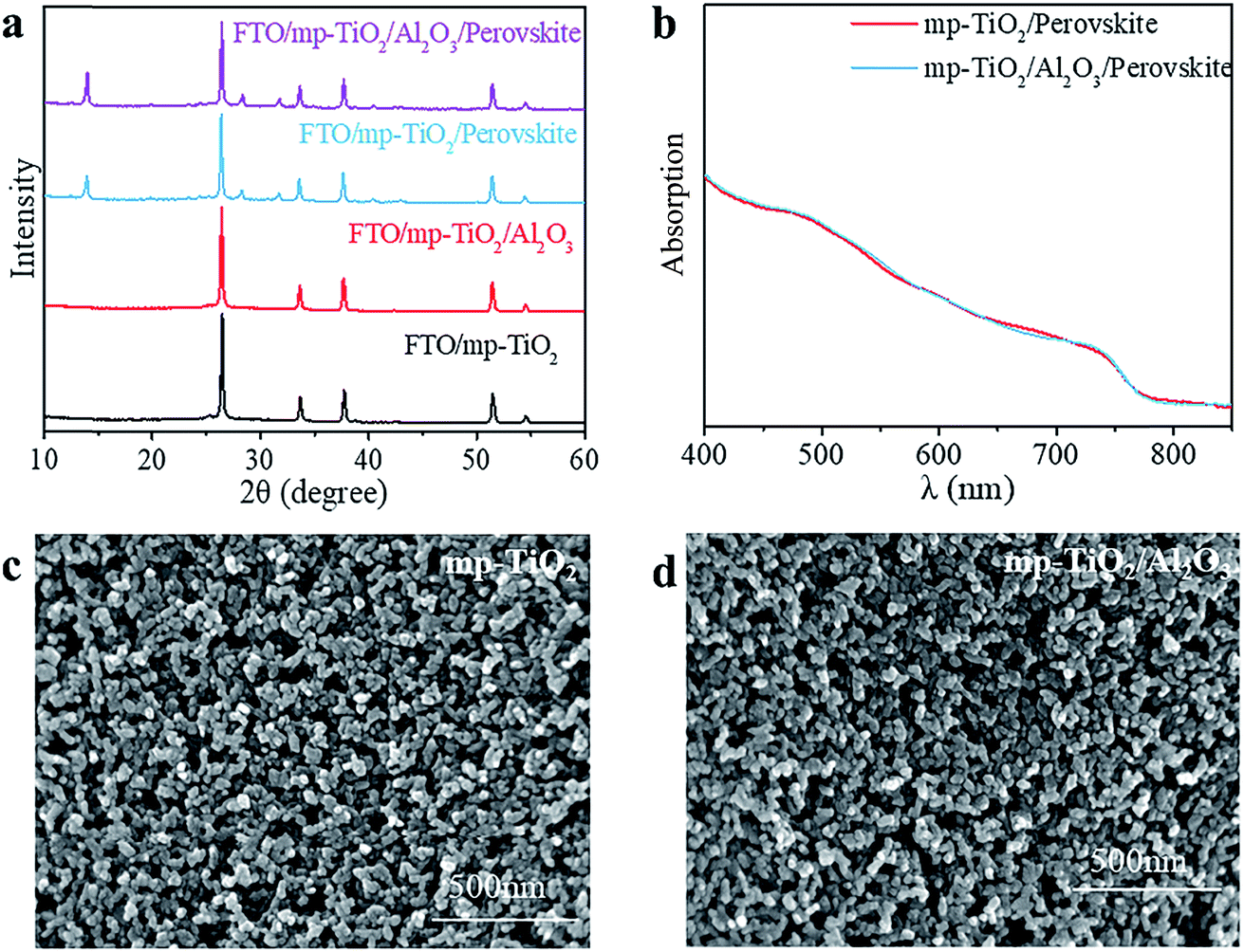 | ||
| Fig. 3 Characterization of films about substrates and perovskite. (a) The XRD spectra of mp-TiO2 and mp-TiO2/Al2O3, the perovskite deposited on these two substrates is also shown. (b) The UV-vis absorption spectra of perovskites on two different substrates. The SEM images of (c) mp-TiO2 and (d) mp-TiO2/Al2O3 on FTO. | ||
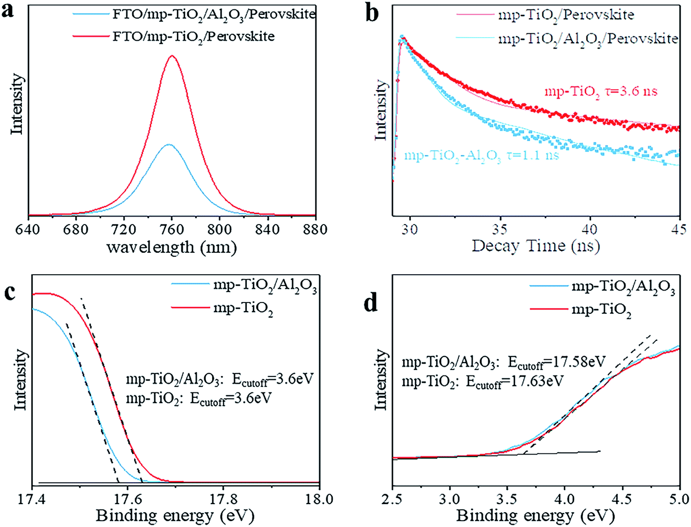 | ||
| Fig. 4 (a) and (b) are the stabilized PL and time-resolved PL spectra for mp-TiO2/perovskite and mp-TiO2/Al2O3/perovskite films. The UPS spectra were recorded for the substrates of mp-TiO2 and mp-TiO2/Al2O3 (c) and (d). | ||
The dark current could reflect the conduction band shift or the energy barrier exhibited at the surface of the electrode.32 In Fig. S5,† the device based on modified mp-TiO2 generates the dark current at a higher forward bias compared with the device based on bare mp-TiO2, indicating that back flow of electrons and carrier recombination at the surface of TiO2/perovskite is suppressed. Thermal Admittance Spectroscopy (TAS) was applied to test the mp-TiO2 film samples and the results are shown in Fig. S6.† Modified TiO2 showed higher defect density at shallow levels and lower defect density at deep levels. The shallow defects act as donors in TiO2 to enhance the carrier density in the TiO2 while the deep level defects would become the recombination centers and lower the VOC and PCE of the devices. We infer that the deep defect density is different in modified TiO2 and bare TiO2. In the intrinsic TiO2 crystal, the lattice suddenly ends on the surface of the crystal so the outmost atoms on the surface of the TiO2 crystal would have an unpaired electron, leaving unsaturated bonds on the lattice surface. These unsaturated bonds are also called “dangling bonds” in semiconductors,33 resulting in deep defect density.34 By modifying with Al2O3, the density of dangling bonds would decrease as a result of the different valences of Ti atoms and Al atoms. Other metal oxides, such as La2O3 and MgO,21,22 have also been used to modify mp-TiO2 and were confirmed to be on the surface of TiO2, and could take effect in the same way. For polymers, special functional groups could also passivate defects at the interface of perovskite and mp-TiO2.16,17 To conclude, the Al2O3 lowered the CBM energy level of TiO2 and showed lower deep defect density, contributing to faster carrier transportation and less carrier recombination. As a result, the VOC and FF of PSC were improved by inserting Al2O3 in a 1.2 μm device, thus increasing the PCE of devices, reaching a comparable PCE with the 3 μm devices.
Conclusions
In summary, we studied a simple spraying pyrolysis method that modified the TiO2 layer with wide-band-gap Al2O3. The insertion of a super thin Al2O3 layer down-shifts the CBM energy level of TiO2. After modification, the recombination is effectively controlled in devices and we also find that the defect density of TiO2 in deep energy levels is reduced. With the help of the thin Al2O3 layer, we successfully reduced the thickness of the ZrO2 layer to 1.2 μm while retaining the photovoltaic performance. The application of the thinner ZrO2 layer in the TiO2/ZrO2/carbon mesoporous scaffold reduced the usage of toxic solvent and Pb to half and improved the reproducibility at the same time. As a result, we are able to achieve a both more cost-efficient and environmentally friendly PSC. Considering that the spraying pyrolysis method is also able to be applied in large-scale manufacturing, this work would promote the commercialization of PSCs with green fabrication processes and lower cost in the future.Conflicts of interest
The authors declare no conflict of interest.Acknowledgements
The authors acknowledge financial support from the National Natural Science Foundation of China (Grant Nos 91733301, 21702069, 91433203, 61474049 and 51502141), the Ministry of Science and Technology of China (2015AA034601), the Fundamental Research Funds for the Central Universities, the Science and Technology Department of Hubei Province (No. 2017AAA190) and the 111 Project (No. B07038). We thank the Analytical and Testing Centre of Huazhong University of Science and Technology (HUST) for performing various characterizations and measurements.Notes and references
- A. Kojima, K. Teshima, Y. Shirai and T. Miyasaka, J. Am. Chem. Soc., 2009, 131, 6050–6051 CrossRef CAS PubMed.
- Best Research-Cell Efficiencies, https://www.nrel.gov/pv/assets/images/efficiency-chart-20180716.jpg.
- Q. Dong, Y. Fang, Y. Shao, P. Mulligan, J. Qiu, L. Cao and J. Huang, Science, 2015, 347, 967–970 CrossRef CAS PubMed.
- G. Xing, N. Mathews, S. Sun, S. S. Lim, Y. M. Lam, M. Grätzel, S. Mhaisalkar and T. C. Sum, Science, 2013, 342, 344–347 CrossRef CAS PubMed.
- D. Shi, V. Adinolfi, R. Comin, M. Yuan, E. Alarousu, A. Buin, Y. Chen, S. Hoogland, A. Rothenberger and K. Katsiev, Science, 2015, 347, 519–522 CrossRef CAS PubMed.
- M. M. Lee, J. Teuscher, T. Miyasaka, T. N. Murakami and H. J. Snaith, Science, 2012, 1228604 Search PubMed.
- S. D. Stranks, G. E. Eperon, G. Grancini, C. Menelaou, M. J. Alcocer, T. Leijtens, L. M. Herz, A. Petrozza and H. J. Snaith, Science, 2013, 342, 341–344 CrossRef CAS PubMed.
- F. Giordano, A. Abate, J. P. C. Baena, M. Saliba, T. Matsui, S. H. Im, S. M. Zakeeruddin, M. K. Nazeeruddin, A. Hagfeldt and M. Graetzel, Nat. Commun., 2016, 7, 10379 CrossRef CAS PubMed.
- Y. Hu, Z. Zhang, A. Mei, Y. Jiang, X. Hou, Q. Wang, K. Du, Y. Rong, Y. Zhou, G. Xu and H. Han, Adv. Mater., 2018, 30, 1705786 CrossRef PubMed.
- A. T. Barrows, A. J. Pearson, C. K. Kwak, A. D. Dunbar, A. R. Buckley and D. G. Lidzey, Energy Environ. Sci., 2014, 7, 2944–2950 RSC.
- K. Hwang, Y. S. Jung, Y. J. Heo, F. H. Scholes, S. E. Watkins, J. Subbiah, D. J. Jones, D. Y. Kim and D. Vak, Adv. Mater., 2015, 27, 1241–1247 CrossRef CAS PubMed.
- W.-Q. Wu, Q. Wang, Y. Fang, Y. Shao, S. Tang, Y. Deng, H. Lu, Y. Liu, T. Li, Z. Yang, A. Gruverman and J. Huang, Nat. Commun., 2018, 9, 1625 CrossRef PubMed.
- Z. Ku, Y. Rong, M. Xu, T. Liu and H. Han, Sci. Rep., 2013, 3, 3132 CrossRef PubMed.
- G. Grancini, C. Roldán-Carmona, I. Zimmermann, E. Mosconi, X. Lee, D. Martineau, S. Narbey, F. Oswald, F. De Angelis, M. Graetzel and M. K. Nazeeruddin, Nat. Commun., 2017, 8, 15684 CrossRef CAS PubMed.
- Y. Hu, S. Si, A. Mei, Y. Rong, H. Liu, X. Li and H. Han, Sol. RRL, 2017, 1, 1600019 CrossRef.
- J. Peng, Y. Wu, W. Ye, D. A. Jacobs, H. Shen, X. Fu, Y. Wan, T. Duong, N. Wu, C. Barugkin, H. T. Nguyen, D. Zhong, J. Li, T. Lu, Y. Liu, M. N. Lockrey, K. J. Weber, K. R. Catchpole and T. P. White, Energy Environ. Sci., 2017, 10, 1792–1800 RSC.
- A. Abrusci, S. D. Stranks, P. Docampo, H.-L. Yip, A. K. Y. Jen and H. J. Snaith, Nano Lett., 2013, 13, 3124–3128 CrossRef CAS PubMed.
- H. P. Dong, Y. Li, S. F. Wang, W. Z. Li, N. Li, X. D. Guo and L. D. Wang, J. Mater. Chem. A, 2015, 3, 9999–10004 RSC.
- Z. A. Page, V. V. Duzhko and T. Emrick, Macromolecules, 2013, 46, 344–351 CrossRef CAS.
- Y. Xiong, X. Zhu, A. Mei, F. Qin, S. Liu, S. Zhang, Y. Jiang, Y. Zhou and H. Han, Sol. RRL, 2018, 1800002 CrossRef.
- S. F. Shaikh, H.-C. Kwon, W. Yang, H. Hwang, H. Lee, E. Lee, S. Ma and J. Moon, J. Mater. Chem. A, 2016, 4, 15478–15485 RSC.
- G. S. Han, H. S. Chung, B. J. Kim, D. H. Kim, J. W. Lee, B. S. Swain, K. Mahmood, J. S. Yoo, N.-G. Park, J. H. Lee and H. S. Jung, J. Mater. Chem. A, 2015, 3, 9160–9164 RSC.
- A. Mei, X. Li, L. Liu, Z. Ku, T. Liu, Y. Rong, M. Xu, M. Hu, J. Chen, Y. Yang, M. Grätzel and H. Han, Science, 2014, 345, 295 CrossRef CAS PubMed.
- A. O. Juma, I. O. Acik, V. Mikli, A. Mere and M. Krunks, Thin Solid Films, 2015, 594, 287–292 CrossRef CAS.
- T. Supasai, N. Henjongchom, I. M. Tang, F. Deng and N. Rujisamphan, Sol. Energy, 2016, 136, 515–524 CrossRef CAS.
- Y. Rong, Y. Hu, S. Ravishankar, H. Liu, X. Hou, Y. Sheng, A. Mei, Q. Wang, D. Li, M. Xu, J. Bisquert and H. Han, Energy Environ. Sci., 2017, 10, 2383–2391 RSC.
- J. M. Marin-Beloqui, L. Lanzetta and E. Palomares, Chem. Mater., 2016, 28, 207–213 CrossRef CAS.
- H. J. Snaith, A. Abate, J. M. Ball, G. E. Eperon, T. Leijtens, N. K. Noel, S. D. Stranks, J. T.-W. Wang, K. Wojciechowski and W. Zhang, J. Phys. Chem. Lett., 2014, 5, 1511–1515 CrossRef CAS PubMed.
- Y. Chen, M. He, J. Peng, Y. Sun and Z. Liang, Adv. Sci., 2016, 3, 1500392 CrossRef PubMed.
- D. Bi, W. Tress, M. I. Dar, P. Gao, J. Luo, C. Renevier, K. Schenk, A. Abate, F. Giordano, J.-P. Correa Baena, J.-D. Decoppet, S. M. Zakeeruddin, M. K. Nazeeruddin, M. Grätzel and A. Hagfeldt, Sci. Adv., 2016, 2, 1501170 Search PubMed.
- T. Liu, L. Liu, M. Hu, Y. Yang, L. Zhang, A. Mei and H. Han, J. Power Sources, 2015, 293, 533–538 CrossRef CAS.
- Y. Diamant, S. G. Chen, O. Melamed and A. Zaban, J. Phys. Chem. B, 2003, 107, 1977–1981 CrossRef CAS.
- R. J. Hamers and J. E. Demuth, Phys. Rev. Lett., 1988, 60, 2527–2530 CrossRef CAS PubMed.
- H. M. Branz and M. Silver, Phys. Rev. B: Condens. Matter Mater. Phys., 1990, 42, 7420–7428 CrossRef CAS.
Footnote |
| † Electronic supplementary information (ESI) available. See DOI: 10.1039/c8se00332g |
| This journal is © The Royal Society of Chemistry 2018 |