
Tin–lead halide perovskites with improved thermal and air stability for efficient all-perovskite tandem solar cells†
Tomas
Leijtens‡
 *ab,
Rohit
Prasanna‡
*ab,
Kevin A.
Bush
a,
Giles E.
Eperon
cd,
James A.
Raiford
e,
Aryeh
Gold-Parker
fg,
Eli J.
Wolf
a,
Simon A.
Swifter
a,
Caleb C.
Boyd
a,
Hsin-Ping
Wang
a,
Michael F.
Toney
g,
Stacey F.
Bent
e and
Michael D.
McGehee
*ah
*ab,
Rohit
Prasanna‡
*ab,
Kevin A.
Bush
a,
Giles E.
Eperon
cd,
James A.
Raiford
e,
Aryeh
Gold-Parker
fg,
Eli J.
Wolf
a,
Simon A.
Swifter
a,
Caleb C.
Boyd
a,
Hsin-Ping
Wang
a,
Michael F.
Toney
g,
Stacey F.
Bent
e and
Michael D.
McGehee
*ah
aDepartment of Materials Science, Stanford University, 476 Lomita Mall, Stanford, CA 94305, USA. E-mail: michael.mcgehee@colorado.edu; toleijtens@gmail.com
bNational Renewable Energy Laboratory, 15013 Denver West Parkway, Golden, CO 80401, USA
cDepartment of Chemistry, University of Washington, Seattle, Washington 98105, USA
dCavendish Laboratory, JJ Thomson Avenue, Cambridge CB3 0HE, UK
eDepartment of Chemical Engineering, Stanford University, Stanford, CA 94305, USA
fDepartment of Chemistry, Stanford University, Stanford, CA 94305, USA
gStanford Synchrotron Radiation Lightsource, SLAC National Accelerator Laboratory, Menlo Park, CA 94025, USA
hDepartment of Chemical Engineering, University of Colorado, Boulder, Colorado 80309, USA
First published on 7th August 2018
Abstract
We report the fabrication of monolithic all-perovskite tandem solar cells with a stabilized power conversion efficiency of 19.1% and demonstrate improved thermal, atmospheric, and operational stability of the tin–lead perovskite (FA0.75Cs0.25Sn0.5Pb0.5I3) used as the low gap absorber. To achieve a high matched current density in the two-terminal tandem, we develop a route to fabricate uniform and thick tin–lead perovskites that enable the two-terminal tandem to attain external quantum efficiencies >80% in the near infrared. By post-processing the as-deposited tin–lead perovskite films with methylammonium chloride vapor, we increase grain sizes to over a micron and boost solar cell open circuit voltage and fill factor. Tin–lead perovskite solar cells made by this method exhibit the most stable operation at maximum power under simulated sunlight of any reported small bandgap perovskite solar cell to date. We show that an unencapsulated tin–lead perovskite solar cell maintains its full performance after 150 hours at 85C in air, which is substantially better than has been observed previously. This work identifies strategies for attaining highly efficient all-perovskite tandem solar cells while maintaining thermal and operational stability.
Introduction
As the single-junction efficiencies of conventional silicon photovoltaics saturate near their theoretical limits, the approach of combining semiconductors that have complementary absorption spectra to make tandem solar cells offers a proven route to further gains in efficiency.1 The most efficient tandem solar cells use epitaxially grown III–V semiconductors to realize 1-sun power conversion efficiencies of over 38%.2–4 However, they rely on expensive and low-throughput deposition methods that hinder their commercial viability. Metal halide perovskites display many of the beneficial optoelectronic qualities of III–V semiconductors5 but can be processed by fast and inexpensive solution-based or vapor-based methods.6–8 All-perovskite tandem solar cells, therefore, are a breakthrough with the potential to realize highly efficient yet low-cost solar cells.9 Mechanically stacked all-perovskite tandems have already been demonstrated with efficiency 23.1%, which is close to surpassing the best single junction perovskite efficiency,10,11 and the next step is to improve the performance of monolithic (two-terminal) tandems, so far demonstrated at 18.5% efficiency.12 A monolithic tandem design offers simpler module integration and lower manufacturing and balance of systems costs while producing comparable energy yield.13ABX3 perovskites with mixtures of tin and lead at the B-site, can have band gaps of 1.2–1.3 eV (ref. 14) and enabled the first all-perovskite tandems with close-to-ideal band gaps.9,14,15 However, tandems based on these perovskites have so far been limited by low quantum efficiencies in the near infrared,16 likely due to difficulty processing optically thick films of tin–lead perovskites with high uniformity and optoelectronic quality. Early reports of tin–lead perovskites reported short carrier lifetimes (under 1 ns), hindering their ability to achieve efficient extraction of photogenerated charge, especially in thick active layers.9,17 Here, we describe methods to process thick and uniform films of a low band gap mixed cation tin–lead perovskite, with carrier lifetimes approaching 0.5 μs. We demonstrate a post-deposition treatment with methylammonium chloride vapor that grows grains and heals cracks in the as-deposited film, boosting device open circuit voltage and fill factor. Rapid post-deposition treatments that “heal” an as-deposited low-quality film are important from an industrial standpoint because they could allow the use of faster and lower-cost deposition methods for the initial film and allow for decoupling of deposition chemistry and methodology from final film morphology. The results of our post-treatment are consistent with observations by Cui et al., who use methylamine vapor exposure to improve the uniformity of a thin film of methylammonium lead iodide,18 and of Yang et al., who report grain growth by Ostwald ripening in a film of methylammonium lead iodide upon treatment with a dilute solution of methylammonium bromide.19
Despite the importance of tin–lead halide perovskites as low band gap semiconductors for tandem solar cells and other applications, concerns have persisted over their stability. There are few reports that rigorously study the stability of tin–lead perovskites. Here, we investigate the degradation of high-performing tin–lead solar cells under operation in light and identify strategies to achieve stable operation. By keeping the tin content at 50% or below, using formamidinium and cesium at the A-site, and employing the post-deposition MACl vapor treatment, we demonstrate tin–lead solar cells with significantly improved stability in continuous operation under illumination. Combining the advances in device efficiency and operational stability, we use our low band gap solar cells in a monolithic all-perovskite tandem solar cell to achieve a stabilized efficiency of 19.1%.
While using tin at the B-site of the perovskite is effective in achieving a low band gap, it introduces a possible instability because tin, unlike lead, is susceptible to oxidation from the 2+ to the 4+ state, resulting in breakdown of the perovskite. Demonstration of stability of the tin–lead subcell under extended periods of elevated temperature is critical to ensuring commercial viability of all-perovskite tandems. Perovskite solar cells with only tin at the B-site have shown extremely poor air stability, often degrading within minutes of air exposure.9,17,20 In a previous study, we showed that alloying tin with lead at the B-site forces the oxidation to occur by a less favorable reaction pathway, thus significantly improving stability toward oxidation.21 For stable operation in the field, solar cells need to withstand extended periods at elevated temperature – this sort of thermal and atmospheric stability has not yet been reported for low band gap tin–lead perovskite solar cells. In this study, using a device capped with a sputtered indium tin oxide (ITO) electrode, we demonstrate maintenance of over 80% of starting efficiency for over 300 hours at 85C in air. Given the concerns around the stability of tin-containing perovskites toward oxidation, the fact that this stability is displayed by a device with no additional encapsulation represents a big step forward in proving the viability of tin–lead perovskites, and by extension, of all-perovskite tandem solar cells.
Results and discussion
Compositional engineering of low band gap perovskites for operational stability
At present, the most efficient low band gap perovskite solar cell is based on the composition FA0.6MA0.4Sn0.6Pb0.4I3, with 40% methylammonium at the A-site and 60% tin at the B-site.14,22 This compound has been reported to attain single-junction efficiencies of over 17%. However, no reports have described its stability under continuous operation. We show in Fig. 1a that when operated at maximum power point under 1-sun illumination, solar cells based on this composition in the same architecture to that of the highest performing devices (ITO/PEDOT:PSS/Perovskite/C60/BCP/Ag) show a steep drop in power output within minutes. This drop is reversed upon leaving the device in the dark. The drop in power output occurs regardless of whether the device is operated in air or in nitrogen (Fig. S1†), suggesting that it is not due to reaction of the perovskite with oxygen.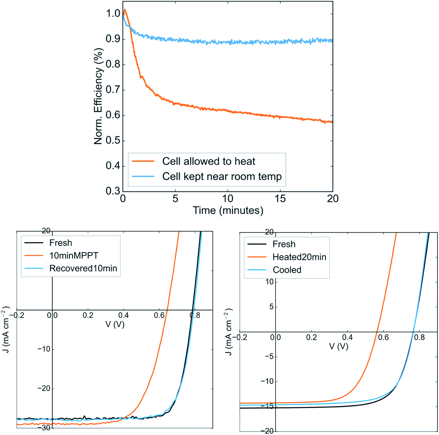 | ||
| Fig. 1 (a) Efficiency of a FA0.6MA0.4Sn0.6Pb0.4I3 solar cell under constant maximum power point tracking with 1-sun illumination in nitrogen, with the solar cell either allowed to heat under illumination or held at a lower temperature by flowing cooled nitrogen gas. (b) JV curves of the FA0.6MA0.4Sn0.6Pb0.4I3 device before and after ten minutes of operation at maximum power point, and after ten minutes of recovery in the dark. (c) JV curves of the FA0.6MA0.4Sn0.6Pb0.4I3 device before and after twenty minutes of heating to 50C, and after ten minutes of cooling and recovery. The lower current in the measurement in (c) is due to use of a lower intensity LED for illumination in the chamber used for heating the solar cell. | ||
Fig. 1b shows the JV curve of the device in its fresh state, after ten minutes of maximum power point tracking, and after ten minutes of recovery in the dark. The efficiency drop during operation is evidently due to a large drop in the open circuit voltage, indicating significantly increased recombination in the device and suggesting the formation of recombination centers in the perovskite. Upon resting in the dark, the voltage is fully recovered. Using a thermocouple attached to the top electrode, we find that during operation under 1-sun illumination, the temperature of the device rises to 50C (Fig. S2†). Interestingly, simply heating the device in the dark to the same temperature results in a drop in the open circuit voltage very similar to that produced upon operation in the light (Fig. 1c). Upon cooling for ten minutes at room temperature, the original JV curve is recovered. The perovskite layer on its own remains stable when heated as a bare film on glass to an even higher temperature (85C) in inert atmosphere, suggesting that there is no intrinsic thermal instability in the perovskite that might result in the efficiency drop (Fig. S3†).
It is typical for the open circuit voltage and power conversion efficiency of a solar to reversibly drop as it heats; the larger density of thermally generated dark carriers results in increased dark saturation current and hence lower voltage. However, in the example of crystalline silicon solar cells, the temperature coefficients have been measured to be 2.3 mV K−1 and 0.65% per K for the open circuit voltage and efficiency respectively,23 while we here observe coefficients around 7.2 mV K−1 and around 1.2% per K despite this material having a larger band gap than silicon. These numbers are far higher than could be expected for standard dark carrier induced losses for a material with a 1.25 eV bandgap. The temperature coefficient of Voc for a more stable perovskite composition (that we describe below) is measured to be only 0.9 mV K−1 (Fig. S4†). This suggests that the PCE drop under operation is largely due to a reversible thermally induced process that results in the formation of recombination centres. If the solar cell is kept at a lower temperature under illumination by flowing cooled nitrogen gas over it, the PCE drop is much less severe (Fig. 1a) – confirming that the instability under operation is indeed thermally induced, rather than light induced or carrier density induced.
We identify two strategies to solve this problem of a thermally induced reversible efficiency drop. In previous work we have shown that reducing the fraction of tin at the B-site is an effective way to stabilize tin–lead perovskites toward oxidation. Fig. 2a shows the efficiency versus time under continuous operation of devices of varying tin content that are otherwise similar. It indicates that this strategy also improves operational stability of devices. Using a tin content of 50% or lower avoids the steep performance drop that the FA0.6MA0.4Sn0.6Pb0.4I3 device shows. Further, replacing the methylammonium cation at the A-site with cesium, which has been shown to be more thermally stable in wider gap lead-based perovskites,24–27 also improves operational stability, even with a high tin content of 60% at the B-site (Fig. 2b). While further investigation is needed to identify the exact mechanisms of the thermally induced PCE drop in solar cells with high tin content, our results point to an effective strategy to make operationally stable tin–lead perovskite devices, which is to use formamidinium and cesium rather than methylammonium at the A-site, and to use 50% or less tin at the B-site.
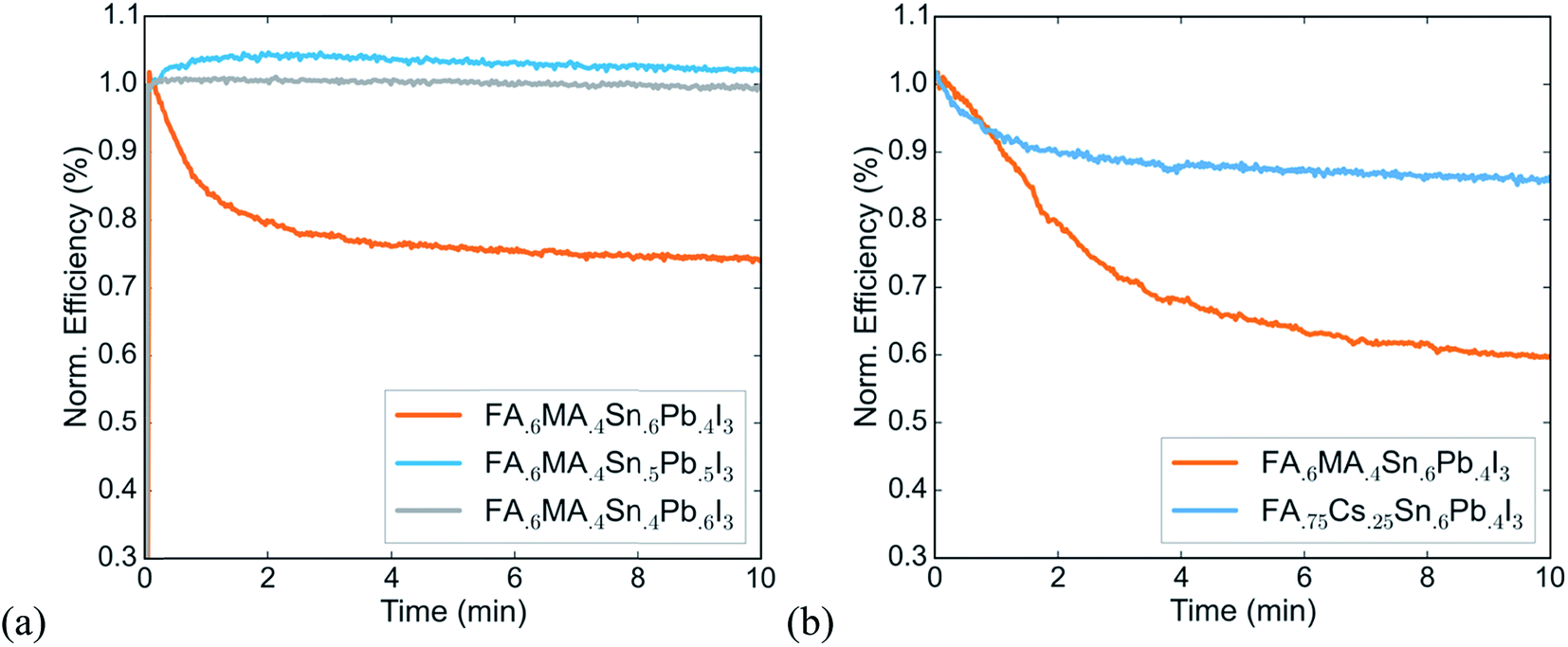 | ||
| Fig. 2 (a) Normalized PCE under continuous operation of formamidinium–methylammonium based tin–lead perovskite solar cells with varying tin content. (b) Normalized PCE under continuous operation of tin–lead perovskite solar cells with either formamidnium–methylammonium or formamidinium–cesium at the A-site, with a constant 60% tin at the B-site. | ||
Using a lower tin content results in a slightly larger band gap, which could compromise the current produced by the low gap cell in a monolithic tandem – but work based on modelling tandem performance under real-world solar spectra has shown that a tandem with a 50%-tin perovskite as the low gap absorber can still realistically reach a PCE of 31%.13 This calculation suggests that the slight compromise of band gap for large gains in stability is worth making and leads us to choose a perovskite with 50% tin at the B-site and a mixture of formamidinium and cesium at the A-site as the low gap absorber in the tandem solar cell. In the next section, we describe fabrication of devices using a FA0.75Cs0.25Sn0.5Pb0.5I3 perovskite and demonstrate that they successfully maintain their PCE over 1-sun maximum power point tracking for over a day, a significant improvement upon operational stability for any tin-containing perovskites reported to date.
Low gap single junction solar cells
High-performing all-perovskite tandem solar cells have been held back by low quantum efficiency in the near infrared due to the difficulty of fabricating optically thick tin–lead perovskite films with good uniformity and long PL lifetime.16 Yan et al. showed a correlation between longer PL lifetimes and larger grain size in films of FA0.6MA0.4Sn0.6Pb0.4I3, suggesting that by optimization of processing, tin lead perovskites can achieve long lifetimes.22 We develop a protocol for making large-grained (∼500 nm) and thick (∼700 nm) films of FA0.75Cs0.25Sn0.5Pb0.5I3 perovskite that show a nearly 1000× improvement in lifetime compared with a small-grained thin film (Fig. 3). The method we use is to spin coat a wet layer of precursor solution and then immerse it in a bath of anisole antisolvent, which quickly extracts the solvent and induces supersaturation and crystallization. Using a low concentration precursor solution (1.1 M) results in a 200 nm-thick film with a large number of small grains (under 100 nm on average), whereas using a higher concentration (2.0 M) results in a film with grain size approaching half a micron and a thickness of 700 nm. The drastic increase in PL lifetime for the thicker large-grained film (Fig. 3c) suggests a step change in recombination rate that might be influenced by grain boundaries, and future work aimed at studying recombination in polycrystalline tin–lead perovskite films is required to fully understand the origin of the large improvement.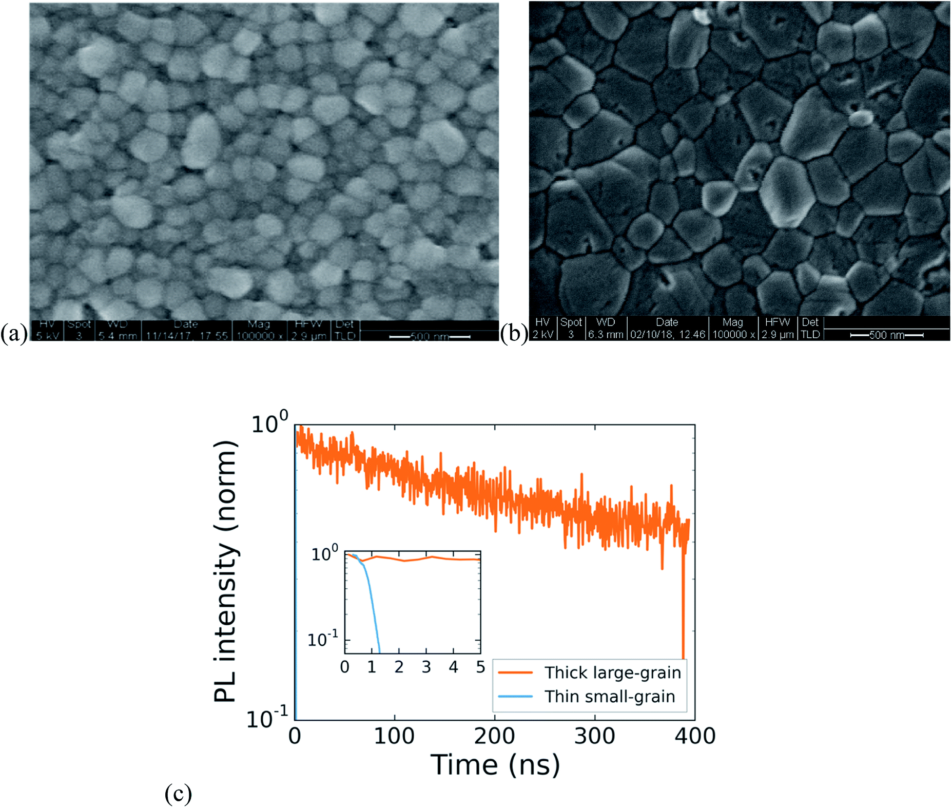 | ||
| Fig. 3 Scanning electron microscope images of films produced by antisolvent immersion method (a) low concentration solution producing a thin small-grained film (b) high concentration solution producing a thick large-grained film. (c) Time-resolved photoluminescence decays measured on the thin small-grained film and thick large-grained film (inset shows a zoom in on the early time region). Thin small-grain and thick large-grain films have the same composition: FA0.75Cs0.25Pb0.5Sn0.5I3. | ||
Single-junction solar cells made using this process to obtain thick large-grained films show a stabilized efficiency of 13.1% (Fig. 4c). While the short circuit current is an impressive 27.2 mA cm−2, the device suffers from low fill factor and open circuit voltage. To address this problem, we expose the as-deposited tin–lead perovskite films to methylammonium chloride (MACl) vapor, followed by a short post-anneal at 150C. This post-treatment results in two effects that are apparent in the SEMs shown in Fig. 4a and b: significant grain growth to form micron-sized grains and healing of cracks that form between grains during crystallization of the as-deposited film. The treatment results in a boost to fill factor and open circuit voltage that raises the efficiency to 15.6% (Fig. 4c).
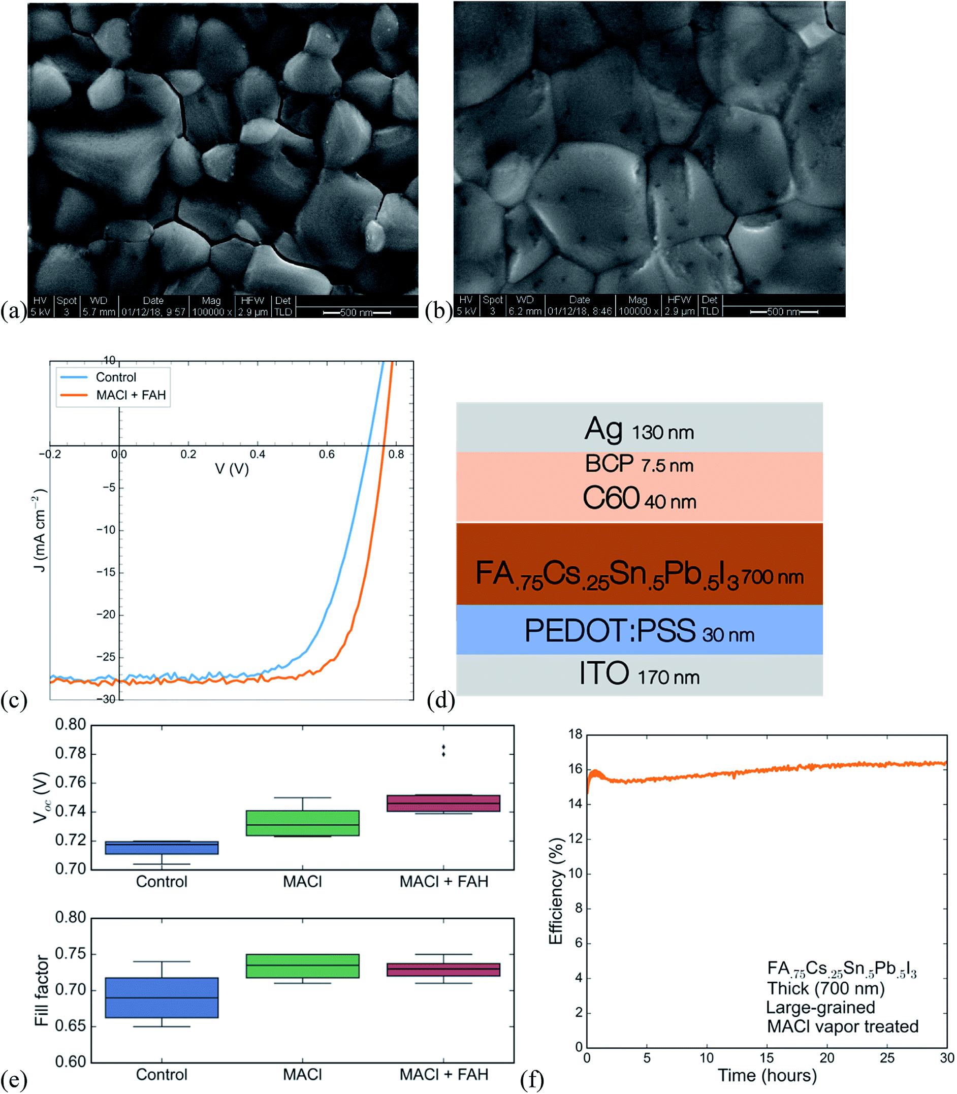 | ||
| Fig. 4 Scanning electron microscope images of (a) untreated and (b) MACl vapor treated films of FA0.75Cs0.25Sn0.5Pb0.5I3 perovskite. (c) JV curves of single junction solar cells based on FA0.75Cs0.25Sn0.5Pb0.5I3 perovskite, with and without MACl vapor treatment and formic acid (FAH) addition. (d) Device schematic of the single junction solar cell. (e) Boxplots comparing Voc and fill factor of devices with and without MACl vapor treatment and formic acid (FAH) addition, where the diamonds represent the highest achieved Voc. (f) Normalized PCE of a FA0.75Cs0.25Sn0.5Pb0.5I3 (thick, large-grained) solar cell under maximum power tracking under constant 1-sun illumination in a nitrogen environment. | ||
XPS spectra of the perovskite films (Fig. S5†) show chlorine at the surface of the treated films. The PL intensity from the perovskite in a device (with contacts) at open circuit is improved upon treating with MACl vapor (Fig. S6†), an effect that is consistent across multiple spots and multiple different devices. The absorption and photoluminescence spectra show a slight increase of around 5 meV in the band gap (Fig. S6 and S7†). However, XRD patterns of films are unchanged upon MACl vapor treatment (Fig. S8†), indicating that there is not enough incorporation of chlorine into the bulk of the perovskite to change the lattice parameter. The increase in PL intensity from the perovskite in a device at open circuit, is likely due to reduction in the amount of nonradiative recombination at the interfaces, which boosts the open circuit voltage.
A recent study found that acidifying the perovskite precursor solution stimulates the formation of dimethylamine from DMF, which aids in dissolving colloids that may form, improves perovskite crystallization and gives a boost to the open circuit voltage.28 Following that report, we use a 5% by volume additive of formic acid, which we find produces a small but reproducible rise in the open circuit voltage (Fig. 4e). Combining the advances of MACl post-treatment and formic acid addition, single junction low gap solar cells reach a stabilized efficiency of 15.6%. This efficiency is maintained without any drop for over thirty hours of operation under continuous 1-sun illumination (Fig. 4f). While the efficiency here is not as high as that of the FA0.6MA0.4Sn0.6Pb0.4I3 devices we and others can make (>17%), the results presented here, and in our previous work on the same composition,9 are the only ones that demonstrate stability for efficient single-junction small bandgap solar cells under operation for more than a few minutes.
Wide band gap cell development
When calculating the theoretical limit in a two-junction tandem solar cell from real absorption profiles, the ideal front cell band gap is between 1.7 and 1.8 eV for a rear cell band gap of 1.27 eV.13 There are a large number of reports on highly efficient solar cells using perovskites with band gaps in the range of 1.50–1.63 eV.26,29,30 A recent compositional study from our group showed that raising the band gap to 1.76 eV by increasing the amount of cesium at the A-site is better than doing so by raising the amount of bromine at the X-site,31 since using higher cesium and lower bromine content slows photoinduced halide segregation (known as the Hoke effect), which leads to trap formation under illumination. We thus use the composition FA0.6Cs0.4Pb(Br0.3I0.7)3 with a band gap of 1.76 eV for the wide gap absorber. Using a thin layer of undoped PTAA and an evaporated bilayer of C60 and BCP as the hole and electron contacts, respectively, the wide gap cell achieves an open circuit voltage of 1.14 V and a stabilized PCE of 14.6% (Fig. 5).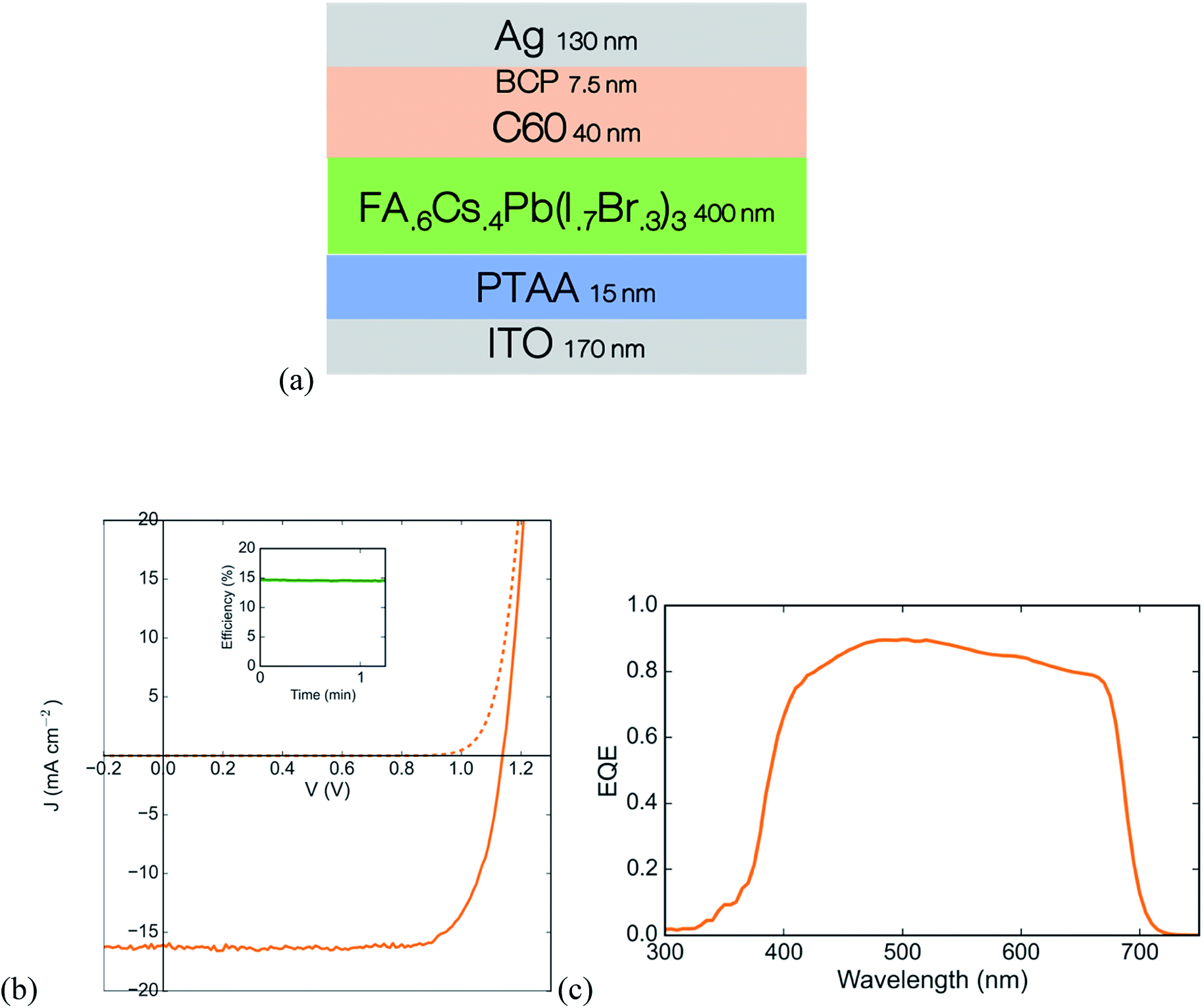 | ||
| Fig. 5 Wide gap single junction solar cell based on a FA0.6Cs0.4Pb(Br0.3I0.7)3 perovskite (a) device stack schematic, (b) JV curve with stabilized maximum power point in the inset, and (c) external quantum efficiency curve. Details of device fabrication are in the ESI.† | ||
All-perovskite tandem solar cells
To fabricate tandem solar cells, we first deposit the wide gap device stack (PTAA/1.76 eV perovskite/C60) on ITO coated glass. As in our previous work,32 we deposit a 10 nm-thick conformal bilayer of tin oxide and zinc-doped tin oxide using atomic layer deposition to serve as an electron selective contact and sputter buffer. This prevents damage during subsequent sputtering of a 120 nm-thick ITO recombination layer. We solution process the low gap perovskite solar cell stack (PEDOT:PSS/FA0.75Cs0.25Sn0.5Pb0.5I3 perovskite/C60/BCP/Ag) directly on this ITO recombination layer to form the rear cell of the tandem.We find that for the ITO recombination layer to be effective in protecting the high band gap cell when we solution-process the low gap device stack over it, it is important to ensure that the wide gap perovskite layer is smooth. Many common recipes for the wide gap perovskite, including one-step spin coating with antisolvent quenching or compressed gas quenching, often produce a wrinkled surface with ridges and valleys several hundred nanometers deep and many microns across (Fig. S9†).33 Solution-processing the low gap subcell over this wrinkled morphology results in extremely poor yield, with most devices being shunted. To avoid this problem, we developed a method based on dynamic interdiffusion of an isopropanol solution of formamidinium iodide (FAI) into a wet layer of cesium iodide, lead iodide, and lead bromide, described fully in the experimental section. This method produces a smooth layer of the wide gap perovskite (Fig. S9†) and enables subsequent solution processing of the low gap subcell.
The JV and EQE curves of the tandem (Fig. 6) demonstrate a stabilized PCE of 19.1%. The tandem shows a matched current density of 14.8 mA cm−2, a significant improvement on the previous best all-perovskite tandem that showed a matched current density of only 12.7 mA cm−2. The higher current is enabled by the thick (700 nm) low gap perovskite layer that generates a quantum efficiency of 80% across much of the near IR. In addition, the current is aided by an antireflective coating, a 190 nm-thick layer of magnesium fluoride deposited on the glass substrate by thermal evaporation (Fig. S10†), and the use of a thin (50 nm) layer of ITO on the substrate to avoid parasitic absorption in the near infrared by free carriers in the high-conductivity ITO.
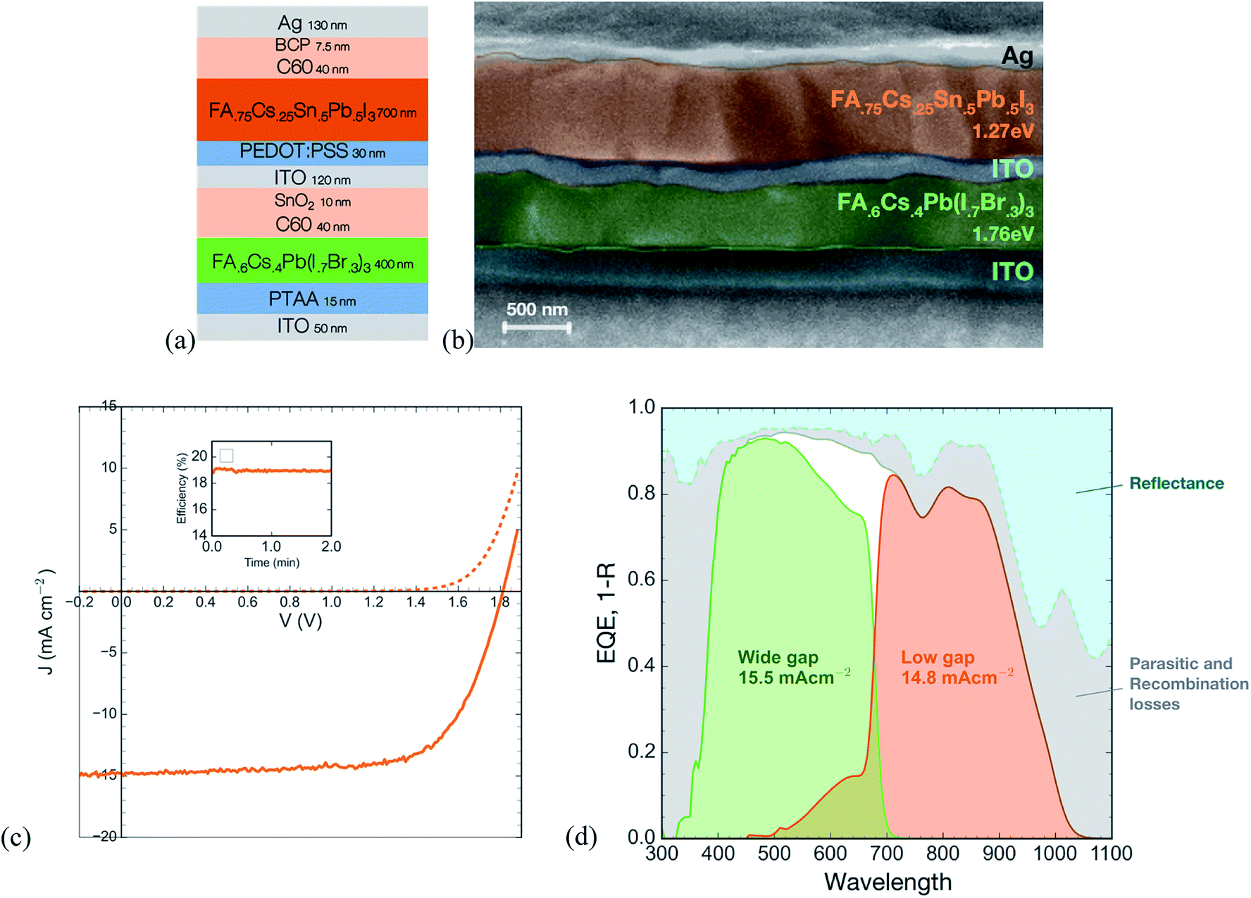 | ||
| Fig. 6 (a) Device stack schematic of the two-junction monolithic tandem (b) cross-sectional SEM image of the tandem solar cell (c) JV curve of the tandem solar cell with stabilized maximum power point in the inset (d) external quantum efficiency of individual subcells in the tandem solar cell and total reflectance. The current density produced by each subcell was calculated by integrating the EQE spectrum across the AM1.5G solar spectrum. | ||
The open circuit voltage of 1.81 V is around 80 mV lower than the sum of the single junction subcells. Out of this loss, around 30 mV is to be expected since the low gap subcell will generate a lower voltage when only half the light is incident on it after having been filtered by the wide gap subcell (calculated using a measured light ideality factor of 1.66, see Fig. S11†). By making electrical contact to the recombination layer, we measure the open circuit voltage of the wide gap subcell to be 1.1 V, which is 50 mV lower than that of a control single junction wide gap device. The discrepancy may be due to a small amount of damage during the ITO sputter or due to solvent penetrating the ITO recombination layer during fabrication of the low gap cell. Further optimization of the ALD buffer layer and the sputter process could prevent this loss. Alternatively, use of a thermally evaporated recombination layer comprising organic small molecules, in combination with an evaporated perovskite layer, has been shown to successfully achieve voltage addition of the two subcells in an all-perovskite tandem.34
Further improvements to tandem efficiency should come from increasing the open circuit voltage of the wide bandgap solar cell, which still suffers from a >0.6 V loss in potential compared to the bandgap. In addition, we plot the absorbance (i.e. 1 – reflectance) of the champion device along with its EQE; the grey area between the two curves represents a combination of light harvesting losses due to parasitic absorption (most likely in the ITO (see Fig. S12†) and PEDOT layers) and possibly from the low bandgap cell having an internal quantum efficiency of slightly lower than 100%. Future work should employ optical modeling to determine the nature of the losses and optimize the device stack to improve the EQE even further.
Thermal stability of tin–lead solar cells
A known degradation mechanism for perovskite solar cells kept at elevated temperature is diffusion of metal from the electrode into the perovskite active layer and diffusion of iodide species to the metal electrode.35–37 To probe the thermal and oxidative stability of the tin–lead perovskite itself, we exclude the metal-diffusion-induced degradation pathway by replacing the metal in the top electrode of our low gap perovskite solar cell with a sputtered ITO layer deposited over a layer of evaporated C60 and atomic layer deposited tin oxide. Not using metal resulted in a lower Jsc and FF because we no longer benefit from a reflective electrode allowing a second pass of light, and the sputtered ITO induces a small amount of series resistance. It is important for future work to develop a good barrier layer to prevent metal diffusion from the electrode.37Fig. 7 shows the evolution of the JV parameters of a FA0.75Cs0.25Sn0.5Pb0.5I3 solar cell upon aging at 85C in air, with no encapsulation. The device was held at open circuit in the dark in an oven between testing. In a remarkable improvement upon any previous report of stability of tin–lead perovskite solar cells, the device maintained its full performance for the first 150 hours and over 80% of its initial PCE for over 300 hours. At longer times, the series resistance started to increase and eventually an S-kink formed in the JV curve, significantly reducing the fill factor (Fig. S13a†). Encouragingly, however, the short circuit current of the solar cell was nearly constant (Fig. S13b†), indicating that there was little, if any, oxidation in the bulk of the perovskite during the air aging, despite the device having been aged in air with no further encapsulation than the ITO top electrode – future studies should aim to identify exactly how effective this sputtered ITO layer is at acting as a barrier to oxygen and stabilizing the tin–lead perovskite. These results are encouraging and suggest that tin–lead perovskite solar cells have enough stability in air to be briefly stored in a factory before they are packaged and that existing low-cost encapsulation technologies will be sufficient to prevent oxidation of the absorber, lifting potential hurdles to the commercialization of all-perovskite tandems.
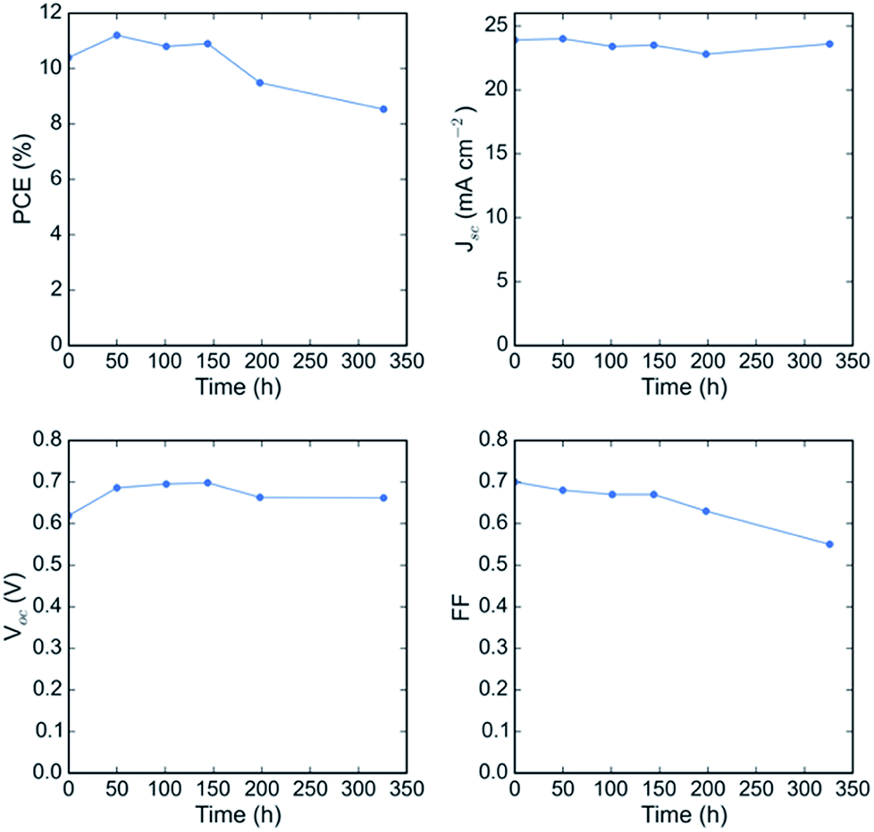 | ||
| Fig. 7 Performance of a FA0.75Cs0.25Sn0.5Pb0.5I3 solar cell with an ITO capping electrode as a function of aging time at 85C in air, with no encapsulation. | ||
Conclusion and outlook
This work has shown that using a 700 nm-thick film of FA0.75Cs0.25Sn0.5Pb0.5I3 with micron-sized grains for the low gap absorber enables efficient all-perovskite tandem solar cells with an EQE of over 80% in the near infrared. These devices also demonstrate good thermal and operational stability when the tin content comprises 50% or less of the B site. While the thermal stability of these devices is a great improvement upon previous reports of tin–lead perovskite thermal stability, the devices do still develop large series resistance and a barrier to charge extraction after 300 hours at 85C in air. We speculate that replacing the acidic and hygroscopic PEDOT:PSS layer with a more stable hole transport layer will be crucial to realizing longer term stability at elevated temperature. What is promising, however, is that the bulk perovskite remains stable with no change in the short-circuit current spectrum observed over 300 hours in air at 85C, suggesting that with suitable engineering of the interfaces and contacts, it is possible to fabricate tin–lead perovskite solar cells that are thermally and operationally stable.Further improvements in the monolithic all-perovskite tandem can be attained by reducing the reflection at 760 nm and past 950 nm in the tandem by optimizing thicknesses and incorporating light trapping schemes such as light-scattering structures in the device stack to minimize reflections.13,38 The fill factor of the tandem solar cell shows room for improvement as well – it is lower than the fill factor predicted by combining the best single junction subcells in series, suggesting some damage during tandem fabrication. Optimizing the sputter process used to deposit the ITO recombination layer or using a better buffer layer to protect from sputter and/or solvent damage are directions to improve the fill factor. Lastly, there is significant room for improvement in the open circuit voltage of the wide gap subcell. With a band gap of 1.76 eV and an open circuit voltage of 1.14 eV, the loss in potential of 0.62 eV is much larger than observed in several reports of perovskite solar cells with smaller band gaps. Devices with larger band gap perovskites, like this one, have often failed to realize improvements in open circuit voltage that are commensurate with their increased band gaps, and identifying the reasons behind this is a high priority for the improvement of all-perovskite tandem solar cells.
Conflicts of interest
There are no conflicts of interest.Acknowledgements
This research was supported by the Office of Naval Research under award number N00014-17-1-2212. Part of this work was performed at the Stanford Nano Shared Facilities (SNSF), supported by the National Science Foundation under award ECCS-1542152. Use of the Stanford Synchrotron Radiation Lightsource, SLAC National Accelerator Laboratory, is supported by the U.S. Department of Energy, Office of Science, Office of Basic Energy Sciences under Contract No. DE-AC02-76SF00515. T. L. is funded by a Marie Sklodowska Curie International Fellowship under grant agreement H2O2IF-GA- 2015-659225. G. E. E. is supported by the European Union's Framework Programme for Research and Innovation Horizon 2020 (2014–2020) under the Marie Skłodowska-Curie Grant Agreement No. 699935. A. G. is supported by NSF GRFP (DGE- 1147470).References
- T. Leijtens, K. A. Bush, R. Prasanna and M. D. McGehee, Opportunities and challenges for tandem solar cells using metal halide perovskite semiconductors, Nat. Energy, 2018, 1 Search PubMed.
- M. A. Green, et al., Solar cell efficiency tables (version 50), Prog. Photovoltaics, 2017, 25, 668–676 Search PubMed.
- P. T. Chiu, et al., 35.8% space and 38.8% terrestrial 5J direct bonded cells, 2014 IEEE 40th Photovolt. Spec. Conf. PVSC, 2014, vol. 2014, pp. 11–13, DOI:10.1109/PVSC.2014.6924957.
- B. M. Kayes, L. Zhang, R. Twist, I. K. Ding and G. S. Higashi, Flexible thin-film tandem solar cells with >30% efficiency, IEEE J. Photovoltaics, 2014, 4, 729–733 Search PubMed.
- R. Brenes, et al., Metal Halide Perovskite Polycrystalline Films Exhibiting Properties of Single Crystals Metal Halide Perovskite Polycrystalline Films Exhibiting Properties of Single Crystals, 2017, pp. 155–167, DOI:10.1016/j.joule.2017.08.006.
- W. S. Yang, et al., High-performance photovoltaic perovskite layers fabricated through intramolecular exchange, Science, 2015, 348, 1234–1237 CrossRef CAS PubMed.
- C. Momblona, et al., Efficient vacuum deposited p-i-n and n-i-p perovskite solar cells employing doped charge transport layers, Energy Environ. Sci., 2016, 9, 3456–3463 RSC.
- Z. Li, et al., Scalable fabrication of perovskite solar cells, Nat. Rev. Mater., 2018, 3, 1–20 CrossRef.
- G. E. Eperon, et al., Perovskite-perovskite tandem photovoltaics with optimized band gaps, Science, 2016, 354, 861–865 CrossRef CAS PubMed.
- D. Zhao, et al., Four-Terminal All-Perovskite Tandem Solar Cells Achieving Power Conversion Efficiencies Exceeding 23%, ACS Energy Lett., 2018, 305–306, DOI:10.1021/acsenergylett.7b01287.
- NREL. Best Research-Cell Efficiencies, https://www.nrel.gov/pv/assets/images/efficiency-chart.png.
- A. Rajagopal, et al., Highly Efficient Perovskite-Perovskite Tandem Solar Cells Reaching 80% of the Theoretical Limit in Photovoltage, Adv. Mater., 2017, 1702140 CrossRef PubMed.
- M. T. Hörantner, et al., The Potential of Multijunction Perovskite Solar Cells, ACS Energy Lett., 2017, 2, 2506–2513 CrossRef.
- R. Prasanna, et al., Band Gap Tuning via Lattice Contraction and Octahedral Tilting in Perovskite Materials for Photovoltaics, J. Am. Chem. Soc., 2017, 139, 11117–11124 CrossRef CAS PubMed.
- B. Zhao, et al., High Open-Circuit Voltages in Tin-Rich Low-Bandgap Perovskite-Based Planar Heterojunction Photovoltaics, Adv. Mater., 2017, 29(2), 1604744 CrossRef PubMed.
- A. Rajagopal, et al., Highly Efficient Perovskite-Perovskite Tandem Solar Cells Reaching 80% of the Theoretical Limit in Photovoltage, Adv. Mater., 2017, 1702140, DOI:10.1002/adma.201702140.
- N. K. Noel, et al., Lead-Free Organic-Inorganic Tin Halide Perovskites for Photovoltaic Applications, Energy Environ. Sci., 2014, 7, 3061–3068 RSC.
- Z. Zhou, et al., Methylamine-Gas-Induced Defect-Healing Behavior of CH3NH3PbI3 Thin Films for Perovskite Solar Cells, Angew. Chem., Int. Ed., 2015, 54, 9705–9709 CrossRef CAS PubMed.
- M. Yang, et al., Facile fabrication of large-grain CH3NH3PbI3–xBrx films for high-efficiency solar cells via CH3NH3Br-selective Ostwald ripening, Nat. Commun., 2016, 7, 12305 CrossRef CAS PubMed.
- F. Hao, C. C. Stoumpos, D. H. Cao, R. P. H. Chang and M. G. Kanatzidis, Lead-free solid-state organic-inorganic halide perovskite solar cells, Nat. Photonics, 2014, 8, 489–494 CrossRef CAS.
- T. Leijtens, R. Prasanna, A. Gold-Parker, M. F. Toney and M. D. McGehee, Mechanism of Tin Oxidation and Stabilization by Lead Substitution in Tin Halide Perovskites, ACS Energy Lett., 2017, 2, 2159–2165 CrossRef CAS.
- D. Zhao, et al., Low-bandgap mixed tin–lead iodide perovskite absorbers with long carrier lifetimes for all-perovskite tandem solar cells, Nat. Energy, 2017, 2, 17018 CrossRef CAS.
- E. Radziemska, The effect of temperature on the power drop in crystalline silicon solar cells, Renewable Energy, 2003, 28, 1–12 CrossRef CAS.
- J. W. Lee, et al., Formamidinium and cesium hybridization for photo- and moisture-stable perovskite solar cell, Adv. Energy Mater., 2015, 5, 1–9 CrossRef.
- D. P. McMeekin, et al., A mixed-cation lead mixed-halide perovskite absorber for tandem solar cells, Science, 2016, 351, 151–155 CrossRef CAS PubMed.
- M. Saliba, et al., Cesium-containing triple cation perovskite solar cells: improved stability, reproducibility and high efficiency, Energy Environ. Sci., 2016, 9, 1989–1997 RSC.
- Z. Li, et al., Stabilizing Perovskite Structures by Tuning Tolerance Factor: Formation of Formamidinium and Cesium Lead Iodide Solid-State Alloys, Chem. Mater., 2016, 28, 284–292 CrossRef CAS.
- N. K. Noel, et al., Unveiling the Influence of pH on the Crystallization of Hybrid Perovskites, Delivering Low Voltage Loss Photovoltaics, Joule, 2017, 1, 328–343 CrossRef CAS.
- W. S. Yang, et al., Iodide management in formamidinium-lead-halide–based perovskite layers for efficient solar cells, Science, 2017, 356, 1376–1379 CrossRef CAS PubMed.
- M. Saliba, et al., Incorporation of rubidium cations into perovskite solar cells improves photovoltaic performance, Science, 2016, 354, 206–209 CrossRef CAS PubMed.
- K. A. Bush, et al., Compositional Engineering for Efficient Wide Band Gap Perovskites with Improved Stability to Photoinduced Phase Segregation, ACS Energy Lett., 2018, 3, 428–435 CrossRef CAS.
- K. A. Bush, et al., 23.6%-Efficient Monolithic Perovskite/Silicon Tandem Solar Cells With Improved Stability, Nat. Energy, 2017, 2, 1–7 Search PubMed.
- K. A. Bush, et al., Controlling Thin-Film Stress and Wrinkling During Perovskite Film Formation, ACS Energy Lett., 2018, 3(6), 1225–1232 CrossRef CAS.
- D. Forgács, et al., Efficient Monolithic Perovskite/Perovskite Tandem Solar Cells, Adv. Energy Mater., 2016, 1602121, DOI:10.1002/aenm.201602121.
- K. Domanski, et al., Not All That Glitters Is Gold: Metal-Migration-Induced Degradation in Perovskite Solar Cells, ACS Nano, 2016, 10, 6306–6314 CrossRef CAS PubMed.
- Y. Kato, et al., Silver Iodide Formation in Methyl Ammonium Lead Iodide Perovskite Solar Cells with Silver Top Electrodes, Adv. Mater. Interfaces, 2015, 2, 2–7 Search PubMed.
- C. C. Boyd, et al., Barrier Design to Prevent Metal-Induced Degradation and Improve Thermal Stability in Perovskite Solar Cells. Manuscript submitted for publication, ACS Energy Lett., 2018, 3, 1772–1778 CrossRef CAS.
- M. T. Hörantner and H. J. Snaith, Predicting and Optimising the Energy Yield of Perovskite-on-Silicon Tandem Solar Cells under Real World Conditions, Energy Environ. Sci., 2017, 10(9), 1983–1993 RSC.
Footnotes |
| † Electronic supplementary information (ESI) available. See DOI: 10.1039/c8se00314a |
| ‡ T. L. and R. P. contributed equally. |
| This journal is © The Royal Society of Chemistry 2018 |