
Design aspects of all atomic layer deposited TiO2–Fe2O3 scaffold-absorber photoanodes for water splitting†
Arto
Hiltunen
 *a,
Tero-Petri
Ruoko
a,
Tomi
Iivonen
b,
Kimmo
Lahtonen
c,
Harri
Ali-Löytty
c,
Essi
Sarlin
d,
Mika
Valden
c,
Markku
Leskelä
b and
Nikolai
Tkachenko
a
*a,
Tero-Petri
Ruoko
a,
Tomi
Iivonen
b,
Kimmo
Lahtonen
c,
Harri
Ali-Löytty
c,
Essi
Sarlin
d,
Mika
Valden
c,
Markku
Leskelä
b and
Nikolai
Tkachenko
a
aLaboratory of Chemistry and Bioengineering, Tampere University of Technology, P.O. Box 541, FI-33101 Tampere, Finland. E-mail: arto.j.hiltunen@tut.fi
bDepartment of Chemistry, University of Helsinki, P.O. Box 55, FI-00014 Helsinki, Finland
cSurface Science Group, Laboratory of Photonics, Tampere University of Technology, P.O. Box 692, FI-33101 Tampere, Finland
dLaboratory of Materials Science, Tampere University of Technology, P.O. Box 589, 33101 Tampere, Finland
First published on 31st July 2018
Abstract
Iron and titanium oxides have attracted substantial attention in photoelectrochemical water splitting applications. However, both materials suffer from intrinsic limitations that constrain the final device performance. In order to overcome the limitations of the two materials alone, their combination has been proposed as a solution to the problems. Here we report on the fabrication of an atomic layer deposited (ALD) Fe2O3 coating on porous ALD-TiO2. Our results show that successful implementation requires complete mixing of the TiO2 and Fe2O3 layers via annealing resulting in the formation of a photoactive iron titanium oxide on the surface. Moreover, we found that incomplete mixing leads to crystallization of Fe2O3 to hematite that is detrimental to the photoelectrochemical performance. IPCE and transient photocurrent measurements performed using UV and visible light excitation confirmed that the iron titanium oxide extends the photocurrent generation to the visible range. These measurements were complemented by transient absorption spectroscopy (TAS), which revealed a new band absent in pristine hematite or anatase TiO2 that we assign to charge transfer within the structure. Taken together, these results provide design guidelines to be considered when aiming to combine TiO2 and Fe2O3 for photoelectrochemical applications.
1 Introduction
Photoelectrochemical hydrogen production from water could provide a clean and inexhaustible source of energy if successfully realized on a large scale.1 For this reason, it has attracted wide interest among researchers ever since the pioneering reports on the topic were published.2,3 Efficient photoelectrochemical water splitting has high demands on the material properties, which have proven to be difficult task to combine all in only one semiconductor. Therefore, a solution to the problem has been sought from material combinations.One strategy to combine two materials is to divide the functions of light absorption and charge transport between an absorber and a high surface area scaffold similarly to dye-sensitized solar cells.4 The scaffolding approach (also known as the host-scaffold/guest-absorber approach) was first demonstrated in water splitting by Sivula et al. where a 60 nm thick hematite layer was deposited on nanostructured WO3.4 Later, demonstrations of a 25 nm thick hematite layer on TiS2 nanonets, a 5 nm thick layer on ZnO nanorods,5 and a few nanometer thick hematite coating on porous ZnO6 have been reported. The suitability of TiO2 as a scaffold for hematite has been studied previously despite the unfavorable band alignment for electron injection. Successful combining of the good electron transport properties of TiO2 and light absorption of iron oxide holds great promise for efficient solar water splitting with safe, abundant and stable materials.
Successful implementation of hematite on TiO2 has been reported to require an underlayer (Nb2O5),7 while at the same time successful realization without an underlayer has also been reported.8 Moreover, annealing the TiO2 with Fe2O3 to create a thin Fe2TiO5 layer on the surface has been proposed to be the mechanism to reach high photocurrents.9 Therefore, the varying experimental results implies that the question of how to combine TiO2 and Fe2O3 in the scaffold/absorber configuration requires further clarification. Furthermore, a recent review tells that the working principles of the Fe2O3–TiO2 heterojunction devices still remain unclear and suggests further investigation on this promising topic.10
The aim of this paper is to establish whether TiO2 is a suitable scaffold for Fe2O3 in the scaffold/absorber configuration. To answer this question, we applied 100, 200 and 400 atomic layer deposition (ALD) cycles of Fe2O3 on porous TiO2. The thicknesses correspond nominally to 5, 10 and 20 nanometers. The composite materials were characterized by scanning electron microscopy (SEM), transmission electron microscopy (TEM), X-ray photoelectron spectroscopy (XPS), Raman spectroscopy, X-ray diffraction (XRD), and they were tested as anodes in a photoelectrochemical (PEC) water splitting cell. The steady-state PEC experiments were complemented by transient absorption (TAS) and transient photocurrent (TPC) measurements to gain insight into the water oxidation dynamics.
Our results show that an annealing step which creates a thin FeTi-oxide layer on the surface is necessary for successful device operation. Importantly, we find that crystallization of ALD-Fe2O3 to hematite will lead to reduced photocurrent once hematite begins to dominate the surface. The growth of hematite can be avoided by using a low number of ALD cycles. For our device architecture, we discover that 100 ALD-cycles is sufficient to increase the absorption of the photoanode without significant hematite crystal growth.
The results presented herein provide new insight into the fabrication of porous TiO2/Fe2O3 photoanodes with the scaffold/absorber technique by clarifying the surface science of the material composition from the perspective of solar water splitting. While this study was carried out by the means of ALD the here presented phenomena and the design principles derived from them are applicable to other fabrication techniques as well.
2 Results and discussion
The TiO2 scaffolds used in this work were fabricated according to a previously published method of ALD on cellulose substrates.11 The resulting weblike TiO2 structure was selected to this study for its large pore size allowing easy penetration of ALD precursors. SEM and TEM images of the TiO2 scaffolds coated with 100, 200 and 400 cycles of ALD-Fe2O3 after annealing are presented in Fig. 1 (see Fig. S1† for a zoomed-out image). TEM images show the hollow tubular structure of the TiO2 scaffold on top of which the ALD-Fe2O3 grow. Based on the SEM images, the application of 100 and 200 iron oxide deposition cycles was found to form individual islands which cover the TiO2 scaffolds throughout. The islands are present already prior to annealing. Increasing the cycle number resulted in increased island sizes that grow large enough to coalesce together. | ||
| Fig. 1 (a–c) SEM images of a TiO2 scaffold coated with 100, 200, and 400 cycles of ALD-Fe2O3, respectively. Images (d–f) are TEM images of the corresponding samples. | ||
X-ray photoelectron spectroscopy was implemented to further characterize the surface of the structure. Table 1 shows the relative elemental concentrations of Ti, Fe and O for the TiO2 sample with 100 cycles of ALD-Fe2O3 coating. Upon annealing at 680 °C the Ti/Fe ratio increases from 1.16 to 2.03, which indicates diffusion of Ti towards the surface. Furthermore, annealing increases the Fe 2p and Ti 2p peak separation by 0.3 eV (Ti 2p peak shifts to lower binding energy), which can be assigned to the formation of a mixed FeTi-oxide. In the studied samples, titanium was found to have oxidation state Ti4+ and iron Fe3+ suggesting the formation of a Fe(III)Ti(IV) oxide. A similar peak shift has been previously observed and associated to the formation of amorphous FexTi1−xOy, where a thin TiO2 coating was deposited over Fe2O3 nanorods.12 The XPS spectra for Fe 2p and Ti 2p energy regions are given in the ESI (Fig. S2†). No Sn was detected on the surface, while the diffusion of tin originating from the underlying FTO has been reported to occur upon annealing at high temperatures.13
| Sample | Concentration, at% (XPS peak position, eV) | ||||
|---|---|---|---|---|---|
| Fe 2p3/2 | Ti 2p3/2 | O 1s | Ti/Fe | Δ(Fe 2p3/2–Ti 2p3/2) | |
| As-deposited | 11.69 (710.62) | 13.53 (458.84) | 74.78 (530.07) | 1.16 | (251.78) |
| Annealed | 7.44 (710.53) | 15.07 (458.43) | 77.49 (529.78) | 2.03 | (252.10) |
X-ray diffraction (XRD) was used to identify the crystal structures. As XRD is a bulk characterization method, all samples indicated crystalline SnO2 from the substrate and anatase TiO2. In the as-deposited condition, the existence of hematite was visible for the sample with 400 ALD cycles, as indicated by its highest intensity {104} peak at 33.3° (see Fig. S3† for the diffractogram). The hematite signal was not detected for the 100 or 200 cycle samples suggesting an amorphous structure. Even though ALD metal oxide films obtained at high temperatures are usually crystalline as-deposited, ultra-thin films (<5 nm) regularly remain amorphous until a critical film thickness value is reached.14 Upon annealing, the high intensity peak of hematite at 33.3° is intensified for the 400 cycles sample which suggests increased degree of crystallinity in the hematite layers compared to the non-annealed ones. Hematite was found in the annealed 100 and 200 cycle samples only in trace amounts.
Raman spectroscopy was used as a complementary experiment to study the annealed samples in more detail. The TiO2 scaffold shows typical anatase signal peaks at 144, 197, 395, 515 and 636 cm−1.15 The hematite peaks16 at 244, 291, 297, 410, 499, 610 cm−1 become clearly visible only after the coating thickness increases up to 400 cycles (Fig. 2). For the 100 and 200 cycle coatings the hematite signal is weak indicating that only a minor amount of ALD-Fe2O3 crystallized to hematite being in line with the XRD results. The LO (longitudinal optical mode) peak at 660 cm−1, which was observed only for the 400 cycle coated sample, has been assigned to disorder within the hematite lattice.17 The appearance of this peak has been also previously observed to appear for high temperature (650 °C) annealed Fe2O3–TiO2 systems and assigned to a reaction between hematite and TiO2.12 This peak is not detected for the 100 and 200 cycle samples as the hematite signal itself is barely visible.
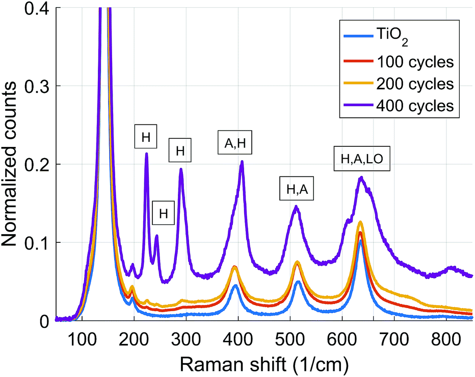 | ||
| Fig. 2 Raman spectra of TiO2 scaffold with varying thickness of ALD-Fe2O3 coating. H: hematite, A: anatase, LO: longitudinal optical mode. | ||
Fig. 3 shows IV-curves for TiO2 scaffold coated with ALD-Fe2O3 along with the bare weblike TiO2 scaffold for comparison. The IV-curves are measured after annealing at 680 °C, which was found to be prerequisite for obtaining reasonable photocurrent from the ALD-Fe2O3 coated samples (see Fig S4† for the IV-curves of as-deposited samples). The TiO2-web shows an IV-curve with photocurrent in the same order of magnitude that has been previously reported for cellulose templated porous ALD-TiO2.18 This allows us to conclude that the web worked as expected and provided a suitable platform for the ALD-Fe2O3 coatings.
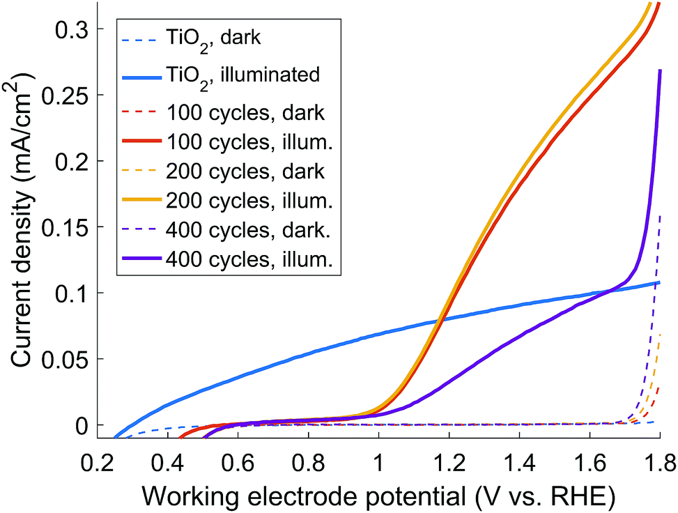 | ||
| Fig. 3 IV-curves of the studied samples. | ||
For the ALD-Fe2O3 samples we found out that the 100 and 200 cycle coatings gave significantly higher photocurrent than the thicker 400 cycle coating. Based on the results obtained by Raman spectroscopy and XRD we can see that the drop of the photocurrent is caused by the crystallization of ALD-Fe2O3 into hematite (see Fig. 2 & 3). This is in accordance with the observation noted previously by Sivula et al.4 and Stefik et al.7 that hematite overlayers on titania results in no photocurrent. This indeed is expected as hematite has a conduction band edge below that of titania, creating an injection barrier for the electrons photogenerated in the hematite layer.7,19 The photoelectrochemical performance of our materials closely matches those published earlier for Fex–TiO2 photoanodes prepared via sol–gel.20
The XPS analysis indicated the formation of an FeTi-oxide layer on the surface upon annealing. When the ALD-Fe2O3 cycle number is kept low, in our case 200 or below, the mixing of ALD-Fe2O3 with Ti during annealing is complete resulting in FeTi-oxide on the surface. This explains why the 100 & 200 cycle coated samples overperform the 400 cycle coated sample, where part of the ALD-Fe2O3 film crystallizes as hematite. Previously, a Fe2TiO5 (pseudobrookite) layer has been synthesized on TiO2 nanotubes by high temperature annealing of electrodeposited Fe2O3.9 More frequently, however, the Fe2TiO5 has been designed to inject electrons to hematite12,21–23 in contrast to what we report here.
Han et al.24 noted on the importance of not covering the whole TiO2 substrate with hematite in their system where the photoactive material was the TiO2. Our system is significantly different as the photoactive material is the mixed FeTi-oxide. To prove that the improved efficiency stems from the increased spectral response, originating from the mixed oxide, incident photon-to-current-efficiency (IPCE) was measured. As expected, the bare TiO2 gives rise to photocurrent only with UV excitation, and no signal with visible light excitation due to the large band gap of the material. However, upon coating of the TiO2 electrode with ALD-Fe2O3 followed by annealing, the spectral response is observed to extend into the visible range up to 600 nm. The IPCE of the hematite containing sample (400 cycles) is reduced compared to the 100 & 200 cycle samples, because hematite cannot contribute to the photocurrent due to the conduction band misalignment. The IPCE spectra are given in the ESI† along with UV-Vis absorption spectra of the materials Fig. S5a and b.†
Transient photocurrent (TPC) decays, measured with UV (355 nm) and visible light (410 nm) laser excitation, complement the steady-state IPCE measurements. The TPC experiment measures the decay of the photocurrent signal created by the laser excitation. The signal is a sum of two decay pathways: the electron–hole recombination and the electron extraction by the external circuit.25,26Fig. 4 shows TPC decays for bare TiO2 and FeTi-oxide normalized relative to the TiO2 355 nm signal. All the presented decays have similar kinetics, which imply that the aforementioned processes are not significantly altered by the coating within the resolution of the experiment. This similarity of the decay curves is evidence that the FeTi-oxide layer is able to inject electrons to the TiO2 network through which the charges diffuse to the FTO contact.
 | ||
| Fig. 4 Photocurrent decays of the ALD-Fe2O3 sensitized (100 cycles, annealed) TiO2 electrodes and the reference TiO2 scaffold. Decays are normalized relative to the TiO2 355 nm signal. | ||
The charge carrier recombination dynamics were studied in the ps–ns timescale using transient absorption spectroscopy of annealed planar 200 cycles ALD-Fe2O3 samples deposited on FTO and TiO2 coated FTO. The 200 cycle sample was selected for the study to achieve high enough absorbance on the planar samples. The excitation wavelength was set to 410 nm to selectively excite only the ALD-Fe2O3 overlayer. In this time-scale the transient absorption is composed of a superposition of the absorptions of both photoexcited holes and electrons.
The negative transient absorption band below 450 nm is due to the bleaching of the ground state absorption. The strong positive absorption band centered at 570–580 nm in the bare hematite sample has previously been assigned to the absorption of photoexcited electrons.27 However, recent investigations of hematite photoanodes under applied bias voltages have revealed a positive absorption at the same wavelength that is formed due to high valent iron-oxo species.28,29 We have previously observed that a bias dependent bleaching of this absorption occurs due to electron transfer into oxidised surface states.30 Thus, we conclude that this absorption band is most probably due to photoexcited holes in the hematite bulk. The decay of the photoexcited electrons is a multiexponential process dominated by recombination and electron trapping.30 The decay of the TAS signal was best fit with three exponential functions with lifetimes of 0.29, 17, and 320 ps (Fig. S6a–c & Table S2†).
The transient absorption spectrum of the ALD-Fe2O3 sample deposited on top of TiO2 and annealed at 680 °C shows the formation of a new broad positive absorption band between 450–680 nm (see Fig. 5b). Neither bare hematite or TiO2 (Fig. S6d†) show a positive transient absorption below 535 nm. Additionally, the globally fitted three exponential decay of the TAS signal now has lifetimes of 0.26, 4.7, and 320 ps. The fastest and slowest components of the decay match those for the bare hematite sample, whereas the middle component is now significantly faster. We determine this new positive absorption band to indicate that electrons have been transferred to the TiO2 layer. The transfer of electrons between the layers explains the faster decay component, and the positive transient absorption spanning from 450 to 680 nm is assigned to the free electrons transferred to the TiO2 layer.31 Interestingly, the ground state bleach observed for the bare hematite sample below 450 nm is not visible for the sample deposited on top of TiO2. This can be due to the transfer of conduction band electrons away from the FeTi-oxide layer leading to the ground state bleach disappearing, further supporting our determination of the electron transfer occurring through the mixed oxide layer, as indicated by the TPC results. Typically, electron transfer between unmixed layers should take place in the picoseconds to nanoseconds timescale. The fact that the change in the TAS spectrum occurs immediately after excitation suggests towards the proposed mixing of the two metal oxide layers.
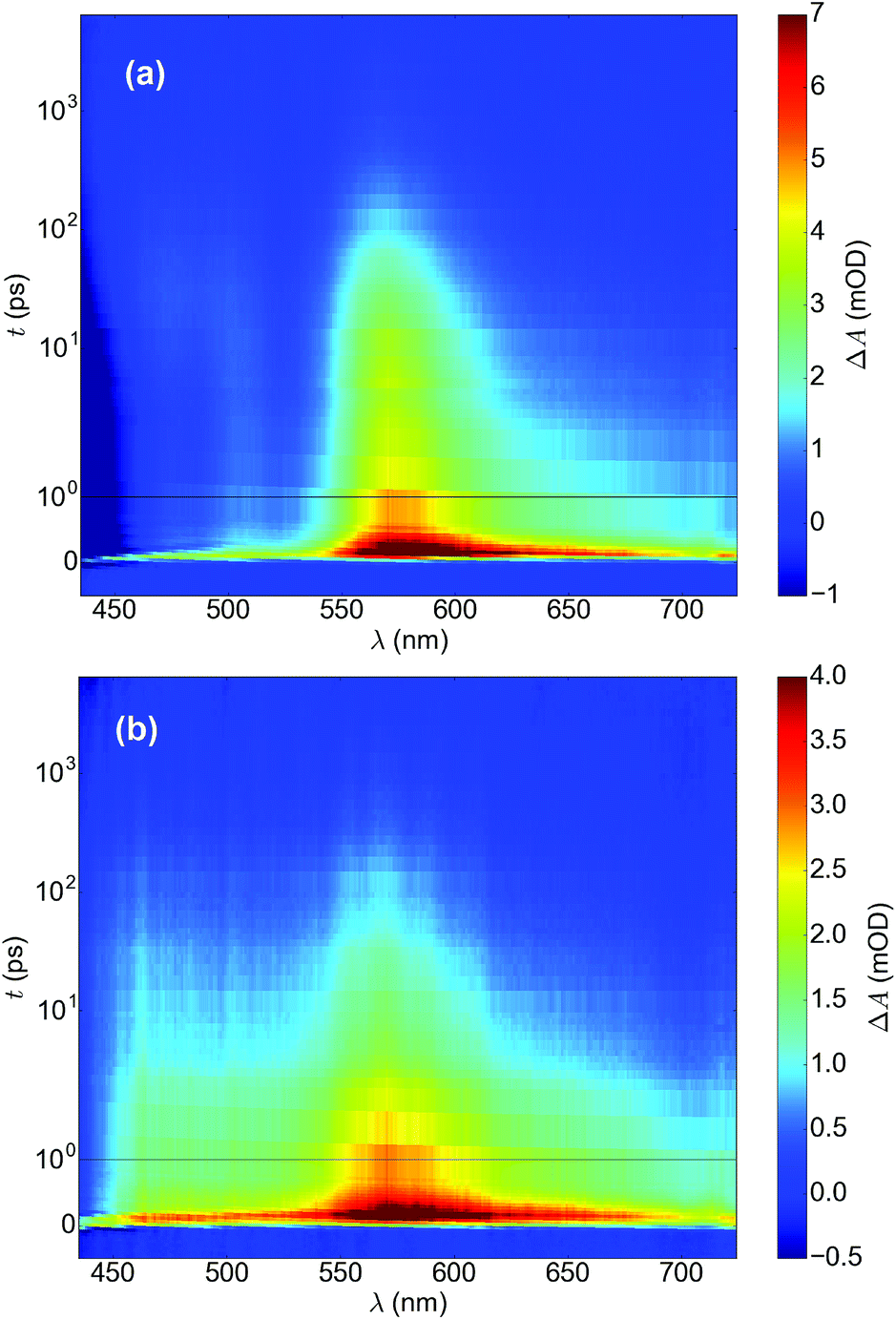 | ||
| Fig. 5 Transient absorption spectra of (a) hematite and (b) FeTi-oxide. Timescale is linear until 1 ps and logarithmic for longer delay times. | ||
3 Conclusions
We have presented a case study on the combination of ALD-TiO2 and thin ALD-Fe2O3 coating for water splitting purposes in a scaffold/absorber configuration. Our results indicate that the condition for the approach is to induce mixing of the Fe2O3 and TiO2 layers at high temperature, resulting in photoactive Fe(III)Ti(IV) oxide on the surface. Furthermore, growth of hematite crystals when a large number of ALD-Fe2O3 cycles was applied resulted in decreased device performance. With 100 and 200 ALD-Fe2O3 cycles crystallization to hematite was avoided, and an increase in the photocurrent over TiO2 was achieved. We consider these results as a indication that ALD-TiO2 and ALD-Fe2O3 is a suitable pair for a host-scaffold/guest-absorber approach when appropriate post-treatments are applied. The tunability of ALD offers vast possibilities for optimization of both the scaffold and coating thicknesses. We propose that follow-up studies should look into applying the same approach on transparent porous TiO2 structures, possibly fabricated by the means of nanocelluloses, with even smaller ALD-Fe2O3 cycle number to reveal the full potential of the approach.4 Experimental
4.1 TiO2 thin film preparation
FTO substrates (TEC 7/2.2, 6–8 ohm sq−1, Solems) were cleaned with detergent and water, and subsequently sonicated in water (Milli-Q), acetone and 2-propanol for 15 min in each solvent. A titanium dioxide compact layer was prepared on the cleaned substrates by spin coating from a titanium isopropoxide precursor solution.32 On these substrates, the porous TiO2 structures were built by coating a cellulose scaffold with 30 nm of TiO2 using atomic layer deposition. The precursor for the ALD-TiO2 was tetrakis(dimethylamido)titanium(IV). After ALD the samples were annealed at 450 °C to crystallize the TiO2 and remove the cellulose from the structure. The details of the method, including the ALD procedure, have been published previously.11Planar samples for transient absorption measurements were prepared by coating FTO substrates with 30 nm of TiO2 using the same ALD procedure as for the cellulose substrates, and annealed at 450 °C. When used as a reference for the ALD-Fe2O3 coated samples, same post-annealings were applied to all.
4.2 Atomic layer deposition of Fe2O3
Hematite thin films were deposited in an F-120 ALD reactor (ASM Microchemistry, Finland) by applying the FeCl3 + H2O-process at 400 °C.33 At this deposition temperature, the growth rate of the hematite thin films on planar substrates is 0.5 Å per cycle as determined via energy dispersive X-ray spectroscopy (EDX) measurements. The EDX spectra were collected using an Oxford INCA 350 microanalysis system connected to a Hitachi S-4800 field emission scanning electron microscope (FESEM). The film thicknesses were calculated from the EDX spectra using the GMRfilm software34 and assuming a bulk density value of 5.3 g cm−3.4.3 Annealing
The high temperature treated samples were annealed at 680 °C for 1 hour using a 20 °C min−1 heating rate. After annealing the samples were taken out of the oven to room temperature while still hot and let cool down.4.4 Scanning electron microscopy
Field emission scanning electron microscopy images (FESEM) images were taken with a Carl Zeiss Ultra 55 instrument. Acceleration voltages varied from 1 to 5 kV.4.5 Transmission electron microscopy
Samples for the transmission electron microscopy study of the structure were prepared by scraping a small amount of the sample in ethanol and casting a drop of the ethanol on a carbon-coated copper grid. After evaporation of ethanol at room temperature, the samples where studied with JEOL TEM 2010 with an acceleration voltage of 200 kV.4.6 X-ray photoelectron spectroscopy
XPS measurements were performed utilizing a non-monochromatized Al Kα X-ray source (hν = 1486.6 eV) and an Argus hemispherical electron spectrometer (Omicron Nanotechnology GmbH) installed in a multifunctional UHV system with a base pressure below 1 × 10⁻¹⁰ mbar.35 The surface elemental concentrations and chemical states of compounds were identified by analyzing high-resolution XPS spectra using CasaXPS software (Version 2.3.16 PR 1.6).36 The binding energy scale was calibrated according to the C 1s C–C/H component at 285.0 eV. After a Shirley-type background subtraction, the peaks were least-squares fitted with a combination of symmetric Gaussian–Lorentzian line shapes. The relative atomic concentrations were calculated using Scofield photoionization cross sections37 and an experimentally measured transmission function of the Argus analyser.4.7 X-ray diffraction
The crystal structures were defined by XRD (Panalytical Empyrean multipurpose diffractometer) with Cu Kα radiation (λ = 1.5405 Å) and a cathode voltage and current of 45 kV and 40 mA, respectively. The samples were scanned over 2θ = 20–90° with a step size of 0.018° and step duration of 19 s per step. The references were ICOD 00-046-1088, ICOD 01-070-6826/ICSD 98-020-2243 and ICSD 98-008-8418 for SnO2, TiO2 and α-Fe2O3, respectively.4.8 Raman spectroscopy
Raman spectra were collected in the backscattering geometry using a confocal Raman microscope equipped with a 532 nm laser source and a 100× objective (NT-MDT Ntegra). The laser power was adjusted to 10 mW at the sample surface using an ND filter. The acquisition time for each measurement was 600 s.4.9 IV-curves and IPCE
The IV-curves were measured using a three electrode setup having the sample as the working electrode, a platinum counter electrode and a Ag/AgCl reference electrode. 0.1 M NaOH was used as the electrolyte contained in a 1 cm × 5 cm quartz cuvette. The IV-curves were recorded with Agilent E5272A source measure unit under AM1.5G 100 mW cm−2 (1 Sun) illumination using Sciencetech SS150 – AAA Solar simulator as the light source. The samples were illuminated through the glass substrate. The light intensity was set with a calibrated reference solar cell from Oriel instruments (model 91150V). The photocurrents were scaled relative to the active area of the samples that was typically a 50 mm2 square. IPCE was measured with the same setup filtering the light trough band pass filters (FKB-VIS-40 from Thorlabs, FWHM 40 nm) that were placed in front of the sample.4.10 UV-Vis absorption
UV-Vis absorption was measured with Shimadzu UV-3600 spectrophotometer. The absorbance was recorded from FTO substrates having a 30 nm ALD-TiO2 layer on top of which ALD-Fe2O3 (100, 200 or 400 cycles) was deposited, and then subsequently annealed at 680 °C. The reference hematite film was prepared directly on the FTO substrate without the TiO2 layer.4.11 Transient photocurrent measurement
The TPC decays were measured with the same three electrode set up described above keeping the working electrode at a potential of 0.5 V vs. Ag/AgCl. A 50 ohm resistor was connected in series with the sample. The sample was excited with laser pulses (355 nm & 410 nm) and the resulting voltage drop over the resistor was measured as a function of time with an oscilloscope (Tektronix TDS 5032B).4.12 Transient absorption spectroscopy
The transient absorption studies were performed using the femtosecond pump-probe method. The primary laser pulses were obtained with a Ti:Sapphire laser (Libra F, Coherent Inc., 800 nm, 100 fs pulse width, repetition rate 1 kHz). Approximately 90% of the fundamental beam was directed to an optical parametric amplifier (Topas C, Light Conversion Ltd.) to produce the excitation pump pulses at 410 nm with approximately 1 mm beam diameter at the sample, attenuated to 0.65–0.8 mW with neutral density filters with 500 Hz repetition rate. The white light probe pulses were obtained directing the remaining fundamental laser beam energy through a motorized translational stage to a Ti:sapphire crystal for white continuum generation. The measurement system (ExciPro, CDP systems) was equipped with a Si CCD detector. The absorbance changes were averaged 2500 times for each delay time, and the whole measurement sequence was performed four times for each sample to minimize variations caused by possible excitation power fluctuations.Conflicts of interest
There are no conflicts to declare.Acknowledgements
M. L. and T. I. thank Academy of Finland (Centre of Excellence in Atomic Layer Deposition), and EU-FP7 Grant “G-PHOTOCAT” (Grant No. 309636). H. A. thanks the Academy of Finland (grant nos 141481, 286713, 310359, and 309920) and the Jenny and Antti Wihuri Foundation. K. L. thanks the Academy of Finland (grant nos 141481 and 286713). A. H. thanks the Finnish Foundation for Technology Promotion. A. H. and T. I. wish to acknowledge the late Dr Leonid Khriachtchev for his assistance in the Raman measurements.References
- T. Hisatomi, J. Kubota and K. Domen, Chem. Soc. Rev., 2014, 43, 7520–7535 RSC.
- A. Fujishima and K. Honda, Nature, 1972, 238, 37 CrossRef PubMed.
- P. J. Boddy, J. Electrochem. Soc., 1968, 115, 199 CrossRef.
- K. Sivula, F. L. Formal and M. Grätzel, Chem. Mater., 2009, 21, 2862–2867 CrossRef.
- Y.-K. Hsu, Y.-C. Chen and Y.-G. Lin, ACS Appl. Mater. Interfaces, 2015, 7, 14157–14162 CrossRef PubMed.
- D. Barreca, G. Carraro, A. Gasparotto, C. Maccato, T. Altantzis, C. Sada, K. Kaunisto, T.-P. Ruoko and S. Bals, Adv. Mater. Interfaces, 2017, 1700161 CrossRef.
- M. Stefik, M. Cornuz, N. Mathews, T. Hisatomi, S. Mhaisalkar and M. Grätzel, Nano Lett., 2012, 12, 5431–5435 CrossRef PubMed.
- L. Liu, Mater. Lett., 2015, 159, 284–288 CrossRef.
- Q. Liu, J. He, T. Yao, Z. Sun, W. Cheng, S. He, Y. Xie, Y. Peng, H. Cheng, Y. Sun, Y. Jiang, F. Hu, Z. Xie, W. Yan, Z. Pan, Z. Wu and S. Wei, Nat. Commun., 2014, 5, 5122 CrossRef PubMed.
- S. Kment, F. Riboni, S. Pausova, L. Wang, L. Wang, H. Han, Z. Hubicka, J. Krysa, P. Schmuki and R. Zboril, Chem. Soc. Rev., 2017, 46, 3716–3769 RSC.
- A. Hiltunen, K. Lahtonen, J. Saari, A. Ojanperä, E. Sarlin, H. Wondraczek, A. Efimov, K. Kaunisto, P. Vivo, C. Maccato, D. Barreca, P. Fardim, N. Tkachenko, M. Valden and H. Lemmetyinen, ChemPhysChem, 2017, 18, 64–71 CrossRef PubMed.
- X. Li, P. S. Bassi, P. P. Boix, Y. Fang and L. H. Wong, ACS Appl. Mater. Interfaces, 2015, 7, 16960–16966 CrossRef PubMed.
- A. Annamalai, P. S. Shinde, A. Subramanian, J. Y. Kim, J. H. Kim, S. H. Choi, J. S. Lee and J. S. Jang, J. Mater. Chem. A, 2015, 3, 5007–5013 RSC.
- V. Miikkulainen, M. Leskelä, M. Ritala and R. Puurunen, J. Appl. Phys., 2013, 113, 021301 CrossRef.
- B. Lafuente, R. T. Downs, H. Yang and N. Stone, The power of databases: the RRUFF project, in Highlights in Mineralogical Crystallography, ed. T. Armbruster and R. M. Danisi, W. De Gruyter, Berlin, Germany, 2015, pp. 1–30 Search PubMed.
- B. Lafuente, R. T. Downs, H. Yang and N. Stone, The power of databases: the RRUFF project, in Highlights in Mineralogical Crystallography, T. Armbruster and R. M. Danisi, W. De Gruyter, Berlin, Germany, 2015, pp. 1–30 Search PubMed.
- A. M. Jubb and H. C. Allen, ACS Appl. Mater. Interfaces, 2010, 2, 2804–2812 CrossRef.
- Z. Li, C. Yao, Y. Yu, Z. Cai and X. Wang, Adv. Mater., 2014, 26, 2262–2267 CrossRef PubMed.
- M. Grätzel, Nature, 2011, 414, 338–344 CrossRef PubMed.
- E. Courtin, G. Baldinozzi, M. T. Sougrati, L. Stievano, C. Sanchez and C. Laberty-Robert, J. Mater. Chem. A, 2014, 2, 6567–6577 RSC.
- L. Wang, N. T. Nguyen, X. Huang, P. Schmuki and Y. Bi, Adv. Funct. Mater., 2017, 27, 1703527 CrossRef.
- J. Deng, X. Lv, J. Liu, H. Zhang, K. Nie, C. Hong, J. Wang, X. Sun, J. Zhong and S.-T. Lee, ACS Nano, 2015, 9, 5348–5356 CrossRef PubMed.
- D. Monllor-Satoca, M. Bartsch, C. Fabrega, A. Genc, S. Reinhard, T. Andreu, J. Arbiol, M. Niederberger and J. R. Morante, Energy Environ. Sci., 2015, 8, 3242–3254 RSC.
- H. Han, F. Riboni, F. Karlicky, S. Kment, A. Goswami, P. Sudhagar, J. Yoo, L. Wang, O. Tomanec, M. Petr, O. Haderka, C. Terashima, A. Fujishima, P. Schmuki and R. Zboril, Nanoscale, 2017, 9, 134–142 RSC.
- B. C. O'Regan and F. Lenzmann, J. Phys. Chem. B, 2004, 108, 4342–4350 CrossRef.
- S. R. Pendlebury, A. J. Cowan, M. Barroso, K. Sivula, J. Ye, M. Grätzel, D. R. Klug, J. Tang and J. R. Durrant, Energy Environ. Sci., 2012, 5, 6304–6312 RSC.
- S. Sorenson, E. Driscoll, S. Haghighat and J. M. Dawlaty, J. Phys. Chem. C, 2014, 118, 23621–23626 CrossRef.
- B. Klahr and T. Hamann, J. Phys. Chem. C, 2014, 118, 10393–10399 CrossRef.
- O. Zandi, A. R. Schon, H. Hajibabaei and T. W. Hamann, Chem. Mater., 2016, 28, 765–771 CrossRef.
- T.-P. Ruoko, K. Kaunisto, M. Bärtsch, J. Pohjola, A. Hiltunen, M. Niederberger, N. V. Tkachenko and H. Lemmetyinen, J. Phys. Chem. Lett., 2015, 6, 2859–2864 CrossRef PubMed.
- T. Yoshihara, R. Katoh, A. Furube, Y. Tamaki, M. Murai, K. Hara, S. Murata, H. Arakawa and M. Tachiya, J. Phys. Chem. B, 2004, 108, 3817–3823 CrossRef.
- S. Pathak, A. Sepe, A. Sadhanala, F. Deschler, A. Haghighirad, N. Sakai, K. C. Goedel, S. D. Stranks, N. Noel, M. Price, S. Hüttner, N. A. Hawkins, R. H. Friend, U. Steiner and H. J. Snaith, ACS Nano, 2015, 9, 2311–2320 CrossRef PubMed.
- J. A. Klug, N. G. Becker, S. C. Riha, A. B. F. Martinson, J. W. Elam, M. J. Pellin and T. Proslier, J. Mater. Chem. A, 2013, 1, 11607–11613 RSC.
- R. A. Waldo, Microbeam Anal., 1988, 23, 310 Search PubMed.
- K. Lahtonen, M. Lampimäki, P. Jussila, M. Hirsimäki and M. Valden, Rev. Sci. Instrum., 2006, 77, 083901 CrossRef.
- N. Fairley, CasaXPS: Spectrum Processing Software for XPS, AES and SIMS, Casa Software Ltd., Cheshire, UK, 2009, version 2.3.16 PR 1.6, http://www.casaxps.com/ Search PubMed.
- J. H. Scofield, J. Electron Spectrosc. Relat. Phenom., 1976, 8, 129–137 CrossRef.
Footnote |
| † Electronic supplementary information (ESI) available: Additional SEM image, XPS data, XRD diffractograms, IV-curves, IPCE, and TAS spectra. See DOI: 10.1039/c8se00252e |
| This journal is © The Royal Society of Chemistry 2018 |